Upload BOM & Gerber

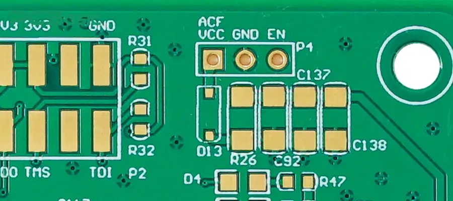
VCC is a typical designation for a device's positive power supply or for an IC power pin. The letter C is repeated in the VCC designation because it is derived from the collector-associated supply notation convention; however, the VCC label by itself does not indicate a universal voltage rating. Always check with the manufacturer for the actual device being powered, the operating voltage range, ground reference, power domain designation of the circuit, and the intended net connection prior to connecting to it.
As an example, a device designated VCC may require 3.3 volts, 5 volts, or another manufacturer-specified voltage. The schematic may also use the VCC designation for a net produced by a regulator, which means that the schematic could say VCC, but in reality the device is using a 3.3 or 5 volt regulator output to power the chip.
Contents
show
What Does VCC Mean in Electronics?
Generally, VCC identifies a positive power supply of a circuit or device. Analog Devices also describes the two C designators as referring to transistor terminals that have traditionally been associated with the supply notation. This is why you may find "VCC" on the IC in question as well as on the schematic net feeding VCC.
VCC is a functional description of an electronic power supply; it is not simply a number. In other words, if a net labeled "3V3" runs to a node on the schematic that is labeled VCC, then it is understood that the design specifies a nominal 3.3 volt power source. The same can be true of designs that use a 5 volt power source; however, neither of these voltages is derived solely from the "VCC" designation.
Each voltage requires a reference point. When a device is cited as VCC = 5 volts, it generally indicates that this particular point within that circuit is 5 volts above the ground or reference point specified in the manufacturer's documentation (i.e., Nexperia's 74HC00/74HCT00 recommended operating conditions specifically indicate this voltage to be referenced to ground at 0 volts).
VCC is the supply potential of a circuit, while GND usually refers to the local ground and return. When looking at a circuit design schematic that mixes ground, earth, chassis, isolation, or a combination thereof, it is important to clarify what the actual grounds in that circuit mean before connecting power or measuring voltage levels.
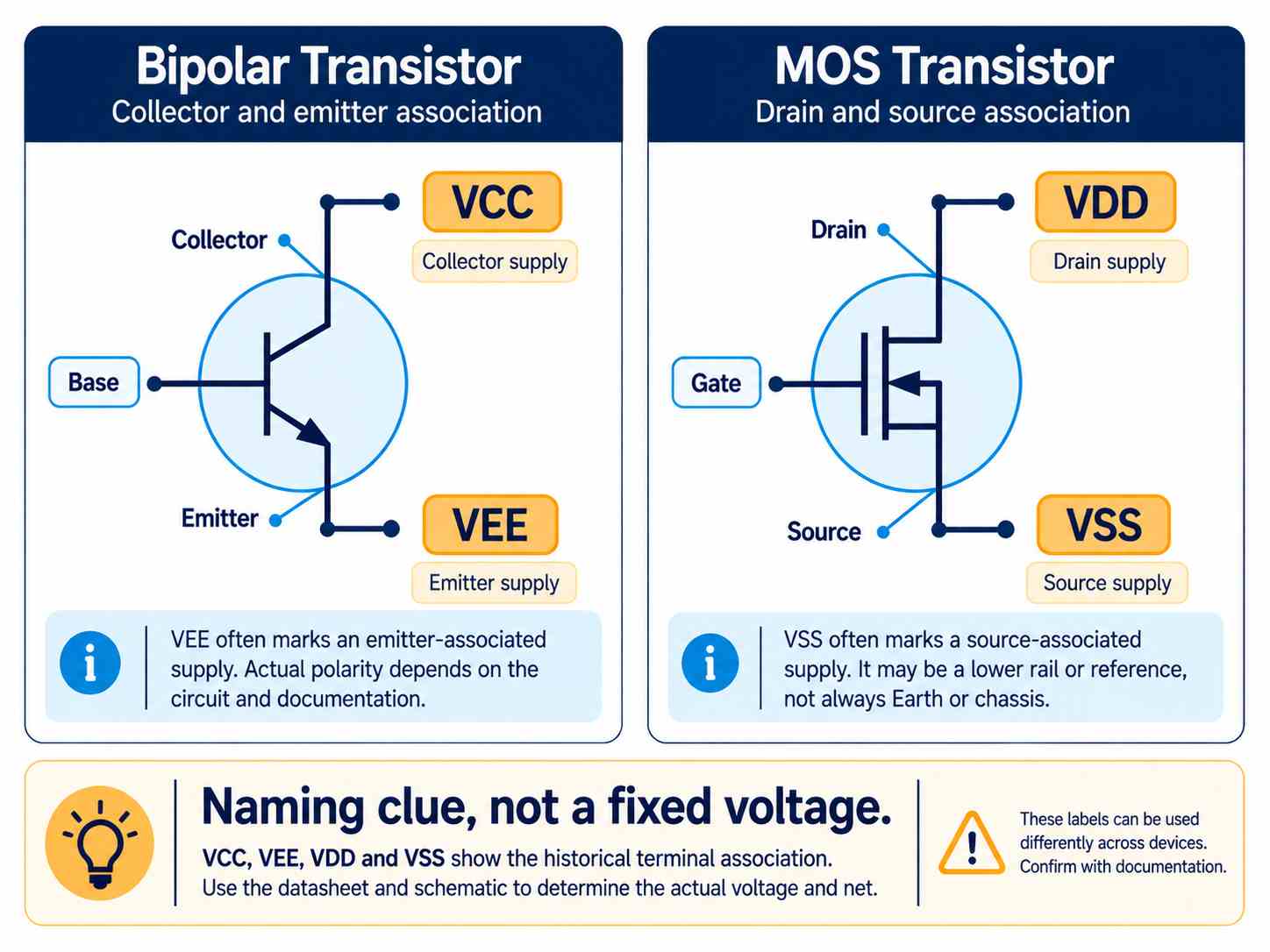
The Repeated C Comes from Collector-Associated Notation
The two Cs are a historical naming clue. In repeated-subscript notation, the doubled subscript distinguishes a supply-rail convention from a single-terminal node voltage such as VC. The letter points to the transistor terminal historically associated with that supply: bipolar circuits led to collector and emitter labels, while field-effect circuits led to drain and source labels. Modern schematics often retain these names even when the device does not expose those internal nodes.
Other manufacturers may use different supply labels, such as VDD, for MOS devices, while either convention may also appear on mixed-signal or digital components. Similarly, many manufacturers may refer to the lower-potential supply as "VEE" or "VSS," while the actual voltage can depend on the circuit's reference point and documentation.
VCC, VDD, and Qualified Rails Are Naming Clues
Qualified names can refer to one of several supply types, including analog, digital, core, I/O, or interface supply. Using this logical method of a "qualified" name indicates the domain of a supply or circuit but does not provide any instruction to short rails together.
Microchip's ATmega328P provides an example of the difference between VCC and AVCC. The VCC pin provides the digital VCC supply for the device. AVCC is a supply for the ADC and for several of the I/O pins. Microchip recommends connecting AVCC to VCC even if the ADC is not used, as well as using a low-pass filter when the ADC is used (as stated in the Microchip ATmega328P datasheet).
This is a requirement for the ATmega328P; it does not apply to all ICs with AVCC. Other ICs may have different supply requirements or timing constraints for AVCC. Please refer to the manufacturer's power section to determine this.
How Do You Find the Correct VCC Voltage?
Never use the package shape, the generic family diagram, or the absolute maximum table for finding the recommended VCC source.
- Write down the manufacturer's name, the complete part number, variant ID, and package type.
- Look up the current version of the manufacturer's datasheet for the specific part number you have.
- Confirm the description of the VCC pin in this datasheet and the number associated with the pin in the package.
- Check the manufacturer's specifications for the recommended range of operating conditions, for example temperature or limits on speed.
- Find the specified reference node and any other power domain that may be separate.
- Compare those operating conditions with the power rail available on the board where the device is mounted and the signal levels of the digital logic that are connected to the device.
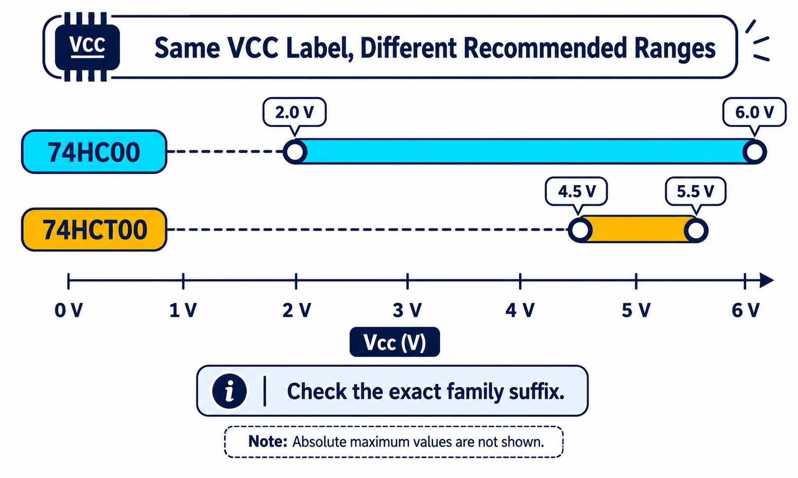
TI describes the VCC voltage for the SN74HC00 as a positive supply voltage. The recommended range for VCC voltage is between two volts (2 V) and six volts (6 V). The absolute maximum rating for VCC voltage as specified in the TI SN74HC00 datasheet is from -0.5 Volts to a maximum of seven volts (7 V). The limits provided in this wider maximum-voltage table are stress limits and are not normal operating conditions.
Nexperia offers a much narrower comparison between the VCC voltage ranges of the 74HC00 and the 74HCT00. The VCC voltage range of the 74HC00 chip is between 2.0 Volts and 6.0 Volts, while the VCC voltage range for the 74HCT00 chip is between 4.5 Volts and 5.5 Volts. Both of these chips contain four two-input NAND gates and share the same pin name, but their family suffixes result in different VCC voltage requirements.
The order in which the evidence has been listed protects against a common error in design procedures: starting with a known, established voltage (e.g., 5 V) and then looking for an IC or module that appears to meet that condition.
What Should a VCC Pin Connect To?
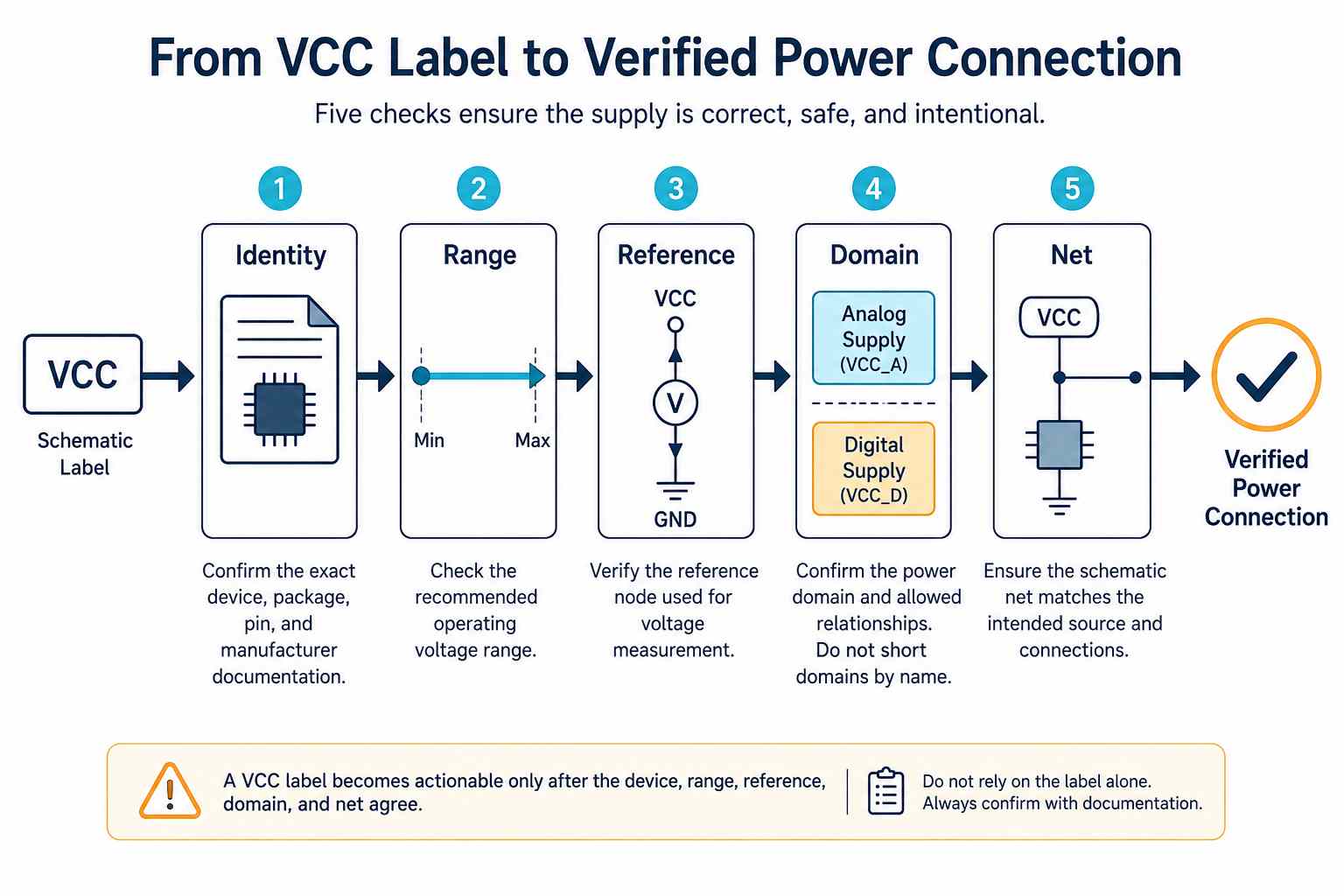
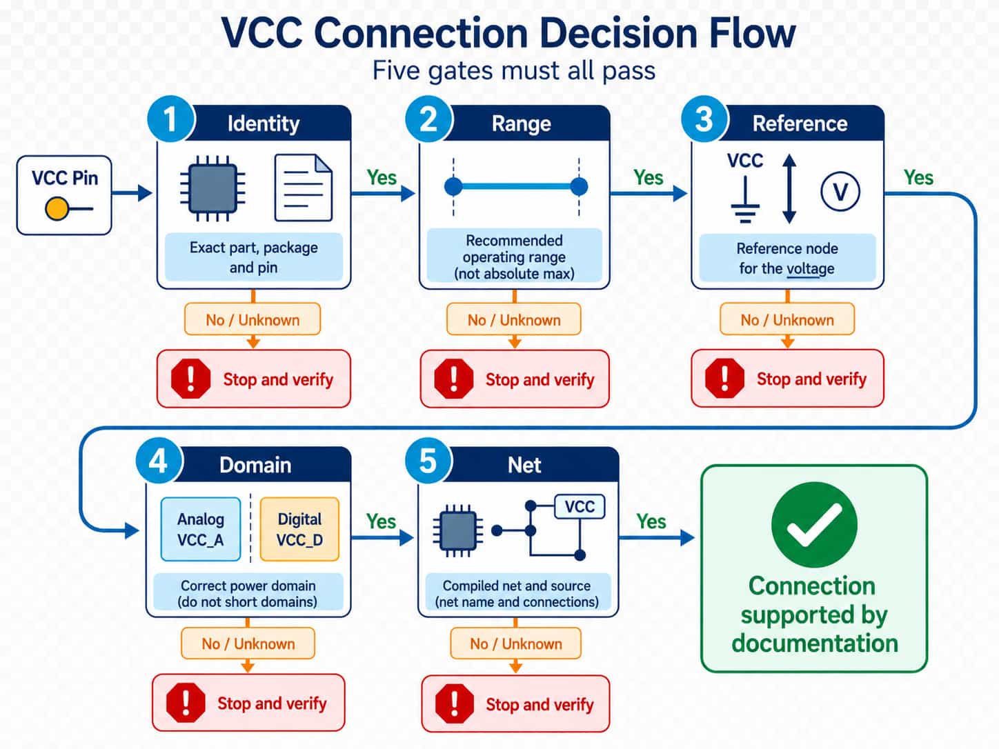
The VCC pin must connect to the power point (i.e., the board rail) that passes five gates represented by identity, operating range, reference, domain, and net. These gates verify the pin, rail, reference, domain, and schematic connectivity. Electrical integrity under the applied load must also be verified.
Gate 1: Identity
Verify the accuracy of the BOM and that you have the correct IC or module; check the manufacturer, package, pin number, and documentation against the BOM. A library symbol named after a broad family is not enough if several variants exist.
Gate 2: Range
Check to make sure the proposed board rail voltage matches the recommended operating conditions for the IC/module. Include application conditions such as temperature, clock rate, and interface restrictions when they are related to the supply voltage.
Gate 3: Reference
Verify the meaning of "zero" in reference to the application. In this case, a nominal 5 V rail with respect to one GND cannot be assumed to have the same reference as a nominal 5 V rail in a different isolated domain.
Gate 4: Domain
Verify which domain (analog, digital, I/O, core, or interface-side) the pin/connection will belong to; verify the required relationships and sequencing before connecting qualified rails.
Gate 5: Net
Follow the schematic label back to the source of the net; verify all information regarding the regulator, connector, net names, hierarchy, and resolved connectivity; verify that the name VCC does not mask an error in the source of the net.
Example: When working on a 74HCT00 that must communicate with a 5 V logic-level device, the Nexperia part permits a voltage range between 4.5 V and 5.5 V. Therefore, a regulated 5 V source can be used as a candidate source for this application. However, to support the connection to the correct pins, the designer must have a valid schematic that shows the output of the regulator driving the correct VCC pins and sharing the intended reference ground.
After the Net Is Correct: Check Supply Integrity
Verify the source's current capacity and tolerance; verify local decoupling components required by the device; verify ripple and transient droop at the supply pins; verify startup or ramp-up requirements; verify any specified sequencing between domains; and verify voltage drop under load. A nominal rail can pass through the schematic and still fail at the device due to voltage drop, load transients, ripple, noise, or an incorrect startup relationship.
When the board is powered but behaves erratically, the designer should use the unexpected symptom to narrow the checks for VCC-related issues rather than replacing components or changing the nominal voltage through guesswork.
When there are multiple power domains that interact or where the resolved connectivity of the design is still uncertain, using a PCB design services review will help resolve the schematic before layout or assembly is performed.
When Do Identical VCC Labels Actually Connect?
If identical power symbols look like they connect together, that does not mean that they do. The EDA naming and hierarchy rules determine how they connect, so don't rely on how they appear; instead, verify that they connect as intended by checking their assigned names, any applicable hierarchy rules, and the resolved connectivity.
KiCad 8 indicates that power symbols are global labels. Power symbols whose power pins have the same name connect across the hierarchy of the schematic. KiCad also allows hidden power-input pins that connect by their pin names, which is a legacy feature that can create connections that are not obvious from regular wires (KiCad Schematic Editor 8.0 documentation).
Altium typically treats power ports that are named identically across the project as connected. However, strict hierarchy settings and the ability to localize power nets may alter the connections. In addition, the net name, not the graphical shape of the power-port symbol, will be used as the identifier in Altium (Altium Circuit Connectivity Documentation).
A short EDA review must be performed before releasing the project:
- Check the effective name of all relevant power objects.
- Inspect the hierarchy and the power-net scope settings.
- Ensure that any hidden or implicit power pins are found.
- Verify and validate the design connectivity and inspect the resolved net membership through the net-inspection functions of the EDA tool.
- Cross-probe each VCC pin to its source and reference.
- Verify that exceptions from the ERC do not prevent you from seeing real VCC power conflicts.
Note that identical symbols may be connected but lead to the wrong regulator, while similar-looking symbols may remain separate due to name differences or hierarchy rules.
Frequently Asked Questions
Q1. Is VCC the same as 5V, 3V3, VIN, or power?
No. Typically, the name VCC signifies the function of the supply and not the amount of voltage (e.g., 5V, 3V3). VIN often designates the voltage coming into a regulator prior to regulation; however, how VIN is used is governed by the module's documentation. Power is the broader definition that can encompass VCC and other supply rails, depending upon how the design requires them to be used. VCC should be connected to one of these nets only after the device requirements have been verified.
Q2. What do VCC+, VCC-, and +VCC mean?
VCC+, VCC-, and +VCC have different meanings based upon the schematic they are in. The existence of a plus sign or a minus sign may denote the polarity of a circuit, a split supply, a channel of the device, or reflect a local naming convention. Do not assume that typography dictates equality or direction; for a device-level comparison, see the LM358P supply-pin definitions of V+ and V- instead of VCC.
Q3. Is VCC the same as HIGH, OUT, or a signal voltage?
No. VCC typically denotes the power rail or supply pin. HIGH is a logic state, and OUT is a type of signal connection. An output-high voltage depends upon factors like VCC, the load itself, and the specifications of the device, but it does not need to match the voltage on the VCC rail. Use interface thresholds and output-characteristic tables to make decisions about signal performance.
Q4. Is VCC always DC and positive?
VCC typically denotes a DC voltage and usually refers to the positive side of the DC voltage relative to its stated reference. A label alone may not guarantee its absolute polarity. Legacy circuits, split supplies, and isolated systems can affect the relationship between the actual voltage and ground on the device; for example, the classic µA741 dual-supply op amp employs VCC+ and VCC− around a signal ground at +15 V and −15 V, so "VCC" is only part of the whole picture since it is only the positive portion of the supply architecture. Furthermore, the output of an isolated DC-DC module's VCC pin is also positive relative to its isolated ground; however, the isolated ground may be tens of volts away from the system ground and the rest of the board. The local reference markers and documentation that accompany each device should be referenced when making statements about VCC or similar terms.
Name the Rail, Then Prove the Connection
Every net should have the verified voltage, source, and reference for that net written on the schematic or design notes so that reviewers can trace each supply pin back to its intended source.
References & Sources
- Vcc – Analog Devices
- SNx4HC00 Quadruple 2-Input NAND Gates – Texas Instruments
- 74HC00; 74HCT00 Quad 2-input NAND gate – Nexperia
- ATmega328P Datasheet – Microchip
- Schematic Editor 8.0 Documentation – KiCad
- Creating Circuit Connectivity in Your Schematics – Altium