Upload BOM & Gerber


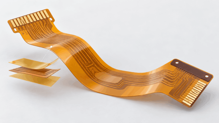
An FPC, also known as a flex circuit, is an electrical interconnect built on a flexible polymer dielectric substrate rather than on a rigid glass-reinforced epoxy laminate. Electrical power and signals flow through copper traces between pads, contacts, and vias like a traditional PCB, but the FPC can follow a controlled three-dimensional path within the installed product.
While “flexible” is a descriptive term for the FPC, it does not imply that the finished circuit can be bent anywhere. There are many mechanical layers that combine copper, dielectric, coverlay, bonding layers, shielding, and stiffening supports. Therefore, designers must consider all elements (i.e., bend location, bend direction, bend radius, bend frequency, and bend support) when designing an FPC.
This is what differentiates flexible PCBs from ribbon cables. Flexible PCBs can accommodate custom printed patterns that may branch, widen, turn, form pads, or connect layers. In contrast, ribbon cables generally contain multiple parallel conductors that have been arranged specifically to mate with a compatible connector.
Contents
show
How Does a Flexible PCB Work?
The FPC is used to provide the same electrical routing function that rigid PCBs perform, but the way that the mechanical stack of the flexible PCB distributes the strain placed on the circuit when it is formed or repeatedly flexed affects how the finished product is assembled and how its electrical characteristics perform.
Polyimide is the most widely used high-performance dielectric material, while polyester and liquid crystal polymer materials are sometimes selected because they are more suitable based on characteristics such as cost, moisture performance, electrical characteristics, and ease of processing. Polyimide alone does not guarantee the life expectancy of the FPC. For example, the Pyralux AP series includes numerous examples of various PCB constructions, including constructions using 18 or 35 µm of copper in conjunction with polyimide dielectric thicknesses from 25 to 150 µm. These product examples do not define the capabilities or limitations of flex PCBs in general.
Copper type is also relevant. Rolled-annealed copper is a popular choice for applications that require repeated movement because this type of copper tends to be more resistant to flex fatigue than standard electrodeposited foils. For static applications, other foil types can be used if the respective stack-up, forming path, and appropriate qualification documentation support them. Designers should compare the unique performance features of flexible PCB material families; therefore, do not treat all polyimide laminates as interchangeable.
Coverlay and surface finish both have differing functions. A coverlay provides a dielectric layer that protects the circuit but intentionally leaves openings in specific locations; surface finish treats exposed metal at these openings. Selection of the surface finish should be based on the type of contact, soldering method, storage conditions, and environment expected for the exposed feature. There is a separate reference available for surface finishes used on PCB contacts and pads.
Types of Flexible PCB
Flex circuits can be classified in three different ways: conductor-layer count, physical architecture, and movement duty. Mixing these categories can result in Design A appearing to be similar to Design B, even though the mechanical characteristics of each design may differ.
Single-Sided, Double-Sided, and Multilayer Flex
Single-sided flexes have one conductor layer and are usually the thinnest type of flex. They are used for simple interconnections. Double-sided flexes have copper applied to both faces of the dielectric material; they may connect to each other through plated vias as well. Multilayer flexes contain three or more conductor layers, allowing for more routing density, shielding or controlled impedance, and multiple crossovers. Each additional conductor, dielectric, bond layer, and shield layer creates additional local thickness; therefore, the total number of layers should be a function of the electrical needs rather than a function of achieving the maximum capability.
Flex, Rigid-Flex, and Semi-Flex
Flex circuits are flexible in that they use a flexible film for the construction of the entire PCB, although small areas may use stiffeners for added rigidity. Rigid-flex boards allow for the use of both rigid and flexible regions in a single PCB construction and allow for components to be mounted on rigid islands with flex areas connecting them. Semi-flex is a method of making a rigid board locally flexible using a thinned or formed area intended for limited movement. Adding a stiffener to a flexible PCB does not inherently create a rigid-flex circuit.
Static and Dynamic Duty
Static flex (flexed to install) circuits are formed during assembly and will remain in their installed position. Dynamic flex circuits are subject to repetitive flexing during operation. The difference between static flex and dynamic flex classifications is not based on layer count: a single-layer circuit may fail quickly due to a poorly controlled dynamic path, while a multilayer circuit may perform reliably in a static bend position if carefully designed.
Advantages and Limitations of Flexible PCBs
Where Flex Creates System-Level Value
Flex circuits utilize flexible materials to create an electrical circuit; these materials can be formed to route through thin, curved, and irregular spaces where a flat rigid PCB cannot fit; a single printed interconnect can also replace multiple wires, cable transitions, and connector pairs. The single circuit can reduce the number of assembly steps and is more easily integrated into a product with fewer separable contacts. In many cases, the conductor pattern of a flex circuit is defined by the artwork, as opposed to a manual wire routing process, which improves repeatability and makes branches, pads, contacts, and test points all part of a single controlled geometry. By reducing conductor mass and the number of loose interconnects, flex circuits can tolerate vibration; however, it is essential to consider the support of the flex path and terminations when designing for these applications.
What Flex Does Not Solve Automatically
The cost to engineer and fabricate a bare flex circuit is typically greater than that of a simple equivalent rigid PCB. The difficulty of properly holding a thin panel flat during the processes of imaging, assembly, and inspection makes it much more challenging compared to using rigid PCBs; rework may require removal and restoration of coverlay or local reinforcement. Support for components, solder joints, and interconnects is essential, as these features should not be allowed to bend without support. Copper can develop fatigue over time as a result of repeated bending, while the addition of a shield or plane intended to improve electrical performance can create a stiffening effect in the bend region.
Flex does not automatically mean that it provides a better thermal solution than rigid PCBs. A thin flex circuit may have a shorter thermal path and more surface area available; however, polyimide will not replace a designed thermal solution. There are multiple factors that determine the actual thermal profile for components, including copper coverage, dielectric thickness, interfaces, airflow, enclosure contact, and losses from the component. The cost of the PCB should also be separated from the system cost; a higher-priced FPC can still lower the total cost of the complete assembly by eliminating connectors, harness assemblies, or assembly operations.
Why Can a Flexible PCB Not Bend Anywhere?
When bending a piece of material, the material on the outside stretches and the material on the inside of the bend compresses, creating a neutral bend axis with a minimum amount of longitudinal strain between them. The position of the neutral bend axis depends on the entire stack of material, including copper, dielectric, coverlay, bonding layers, shields, and reinforcements. The neutral bend axis is not a unique physical layer.

Feature placement in the layout of flexible PCBs will affect the localized strain in each of the features. The trace region does not behave like a pad, plated via, termination, component, or stiffener edge. Therefore, flexible PCB designers should delineate their designs into three distinct mechanical zones:
- Bend zone: this is the area of the PCB that is intended to be controlled as it forms during installation or moves while in use; match the total stack, trace path, geometry, and clearances of the PCB to the expected motion.
- Supported zone: this area is expected to be stable while supporting contact surfaces, components, fasteners, and insertion loads; a portion of the total PCB structure, in the form of a stiffener, housing, or rigid section, contributes to achieving this support.
- Transition zone: this region marks the transition between a supported and flexible area and requires smooth geometry and sufficient separation between features to prevent concentrated loading in these zones.
When bending a PCB centered on a component, pad, via, or stiffener edge, the bend creates concentrated strain on the least tolerant feature of those structures. Creating sharp creases or undefined folds can have the same result; both the crease location and bending radius are uncontrolled. Using a forming tool or fixture can enable the manufacturer to create a one-time bend that can be repeatedly produced, without it having to be engineered as a dynamic flex design.
Flex-to-Install and Dynamic Flex Need Different Designs
The primary function of a flex-to-install circuit is to establish its shape while assembling the product and remain restrained within that shape. Dynamic circuits undergo repeated movement throughout operation and therefore require a controlled motion loop, restraint system, environment, cycle target, and definition of failure for the dynamic duty, not simply an enlarged nominal bend radius.
A lifetime or bend claim is only relevant when it specifies the tested construction and the environment in which it was tested. The review document should detail the complete local stack; the bend angle and inside radius; the direction relative to the conductor pattern; static or dynamic duty; expected number of cycles and frequency; temperature and humidity; vibration or torsion; the electrical or mechanical failure criteria; and any features that must not be present in the bend zone. For an example of what expected cycles mean in practice, a minimum of 100,000 cycles is commonly targeted for IPC-6013 qualification testing of dynamic flex circuits at the rated radius without an open circuit or defined resistance shift, although the actual requirement is defined in the individual product qualification plan.
Flexible PCB Bend and Routing Rules
These rules are design checks and should not be regarded as absolute limits on manufacturing. The final geometry will be defined by the released stack and by the required reliability level.

- Before routing, define the location of the bend line and the associated motion path. A design sketch or drawing should indicate where the forming occurs, the direction of motion, and whether it will be a one-time or repeated bend or movement.
- Route conductors smoothly through the bend area. The traces should cross the bend line at a 90-degree angle instead of running diagonally across the line, and sharp corners or changes in width in the active area should be avoided.
- Any rigid or solid features should not be included in a dynamic bend. Pads, vias, components, connector contacts, or the edges of stiffeners must be kept away from the dynamic bend area unless the qualified construction specifically permits otherwise.
- Minimize any instances of stiffness discontinuities. Rounded outline corners, gradual changes in width, and the use of balanced copper or controlled coverlay or shield transitions will help distribute strain.
- Keep conductor stacking in multilayer flex under review. Staggering of conductors could help minimize the effects of the I-beam behaviour that can occur with aligned conductors directly above one another during bending.
- Use the bend ratio as a descriptor and not as a guarantee. The bend ratio equals the inside bend radius divided by the finished flex thickness; typical published guidance for static one-time bends ranges from roughly 6-12 times thickness, whereas guidance for more demanding dynamic designs can be as high as 100 times thickness or greater; however, acceptable values will vary depending on parameters such as layer count, copper type, bend angle, motion duty, and validation conditions.
- Qualify the installed assembly after it has been built. The continuity of the bare board does not confirm whether the completed assembly will endure loads from connectors, housing interference, torsion, vibration, or its intended number of flexing cycles.
These principles align with the mechanical examples in Designing a Flex Circuit for Flexibility. The subjects discussed include the position of the neutral axis, bend ratios, plated-hole placement, conductor direction, layer stacking, and unbonded regions in relation to flexible circuit constructions.
Which Interconnect Architecture Fits the Job?
A flexible PCB is not automatically a better alternative to a rigid PCB, flat cable, or wire harness. The selection of an interconnect method depends on the type of components being used, the nature of the motion of these components, how they will be connected, what type of three-dimensional routing may be necessary, the access required for servicing, and the total complexity of the final assembly.

A local stiffener is a support, not a rigid-flex construction. The Amphenol FFC/FPC connector guide separates the “parallel-conductor” FFC from the printed FPC families even though they may use similar connector families.
- A sensor tail wraps once around an enclosure wall and then remains fixed. If the bend and supported contacts are defined, a flex-to-install FPC can replace a rigid board with a cable.
- Displays that move on a hinge during operation can use a dynamic FPC; however, the design will include several primary inputs including the motion loop, stack, restraint, cycle target, and validation plan.
- Two fixed-position boards that require a removable straight jumper can be configured using either a connectorized FFC or wire assembly, which may provide a simpler and more serviceable solution than a custom FPC.
The physical differences between these options are also detailed in the guide to flex and rigid-flex PCB structures.
Flexible PCB Application Scenarios
Camera and Display Modules
Camera and display modules tend to use a thin interconnect that leaves a small sensor or display, passes through a narrow enclosure path, and terminates at the main circuit board connector. This flex circuit may bend only during installation; the contact area will still need a stiffener for insertion and retention loads. In addition, the design must ensure that the final enclosure does not pinch the tail or force the bend onto the stiffener edge; here, the value of FPC is controlled three-dimensional routing and repeatable contact geometry, not repeated flexing.
Printer Heads and Robotic Motion
When a printer carriage, pick-and-place head, or small robotic axis is subjected to repeated motion over a specified distance, the flex circuit is typically routed in a guided loop to allow the bend to migrate in a controlled manner, preventing creasing at a single point.
Flex fatigue is affected by copper type, finished thickness, conductor direction, loop geometry, acceleration, temperature, and cycle count. The design should validate the flex circuit by reproducing the real excursion and restraint system of the installed device, as flexing the sample by hand provides no representative information on installed performance or service life.
Medical Probes and Wearable Electronics
Ultrasound probes, body-worn sensors, and compact monitoring devices require thin routing to follow a curved enclosure and minimize the overall weight of the device when worn by the user. Some designs are static after assembly, while cables and hinged modules may move throughout use.
The flexible PCB itself does not establish biocompatibility or environmental resistance; various attributes such as encapsulation, housing seals, cleaning chemicals, sweat exposure, cable strain relief, and the actual motion path must be evaluated in assembled devices.
Automotive Sensors and Controls
Automotive applications use flex circuits within a constrained assembly where sensors, switches, lighting, or controls exist on separate planes. Printed electrical patterns can assist in reducing loose wiring and keeping contact locations repeatable; however, environmental conditions including temperature cycling, vibration, connector loading, fluids, and installation variability will continue to exist as system requirements. Automotive use, such as steering, seat, door, or actuator applications, may also combine occasional service movement with continuous vibrational loading; therefore, flex circuits should be evaluated within their final restrained housings rather than considered solely as bare flexible strips.
How Are Flexible PCBs Manufactured?
Bare-board construction creates the printed interconnect before any components are mounted. The exact route depends on the number of layers, material system, via structure, surface finish, and final outline method.

- Prepare the selected copper-clad flexible laminate and create the image of the conductor pattern.
- Use chemical etching or other formation techniques to make the copper trace pattern, and inspect it for geometry and registration.
- When the construction specifies the need for via drilling and plating, drill and plate vias or interlayer connections.
- Laminate the coverlay, bondply, additional conductor layers, shields, or stiffeners according to the released stack.
- Open the pad/contact areas and apply the specified surface finish to the exposed metal.
- Form the final outline and verify the visual, dimensional and electrical characteristics against the acceptance requirements.
Methods for producing coverlay windows and final outlines include die cutting, punching, routing, or laser processing, dependent upon material type, geometry, tolerance, tooling economics, and production volume. Each method affects edge condition and registration; however, there is no one cutting method that ensures circuit reliability.
Electrical testing is useful for detecting open and short conditions in bare circuits, but does not replace inspection of coverlay registration, plated structures, finish, final outline quality, or project-specific mechanical and environmental validation.
Where Fabrication Ends and Assembly Begins
A bare FPC contains a patterned conductive and insulating structure without any mounted electronic components. The flex PCBA is produced by the addition of components, connectors, or hardware; therefore, there is a boundary where the fabrication process and the assembly process diverge, with distinct fixtures, process controls, defect types, and acceptance evidence for each process.
Assembly of the flex PCB requires that a thin circuit be held flat enough to enable printing and placement; it must also be supported through the soldering process and prevent solder joints or components from entering an active bend. Carrier design, warpage control, paste transfer, reflow support, inspection, and post-assembly handling should all be considered as part of the flex PCB assembly process rather than the bare-board manufacturing process.
Standards and Validation
IPC-2223F establishes sectional design requirements for Flexible and Rigid-Flexible Printed Boards, while IPC-6013F addresses Qualification and Performance Requirements. The three separate documents IPC-4202, IPC-4203, and IPC-4204 cover material families for flex PCB fabrication, and the purchase drawings or qualification plan should indicate the applicable document and revision numbers rather than simply indicate that the circuit was manufactured to IPC standards.
Standards serve as a common basis for design and acceptance criteria; however, the application definition is never replaced by the use of standards. Even a reliable flex circuit requires a released stack, defined bend zones, motion duty, environment, feature keepouts, assembly restraints, and a test method with an explicit failure criterion.
References & Sources
- FPC Sample Kit Technical Guide – Molex
- IPC-2223 Revision F – Global Electronics Association
- IPC-6013 Revision F – Global Electronics Association
- Bending, Forming and Flexing Printed Circuits – IPC
- Designing a Flex Circuit for Flexibility – Minco
- Pyralux AP Flexible Circuit Materials – DuPont
- Pyralux LF Coverlay Data Sheet – DuPont
- Felios Flexible Circuit Board Materials – Panasonic
- Flexible Circuit Design Guide – All Flex
- FFC and FPC Connectors – Amphenol Communications Solutions
- Flexible PCB Explained: Smart Choice for Modern Designs – AIVON