Upload BOM & Gerber
-
Mobile: +86 13312967631
-
Email: sales@sugaintl.com

PCB & PCBA X-Ray Inspection Services
Traceable X-Ray Inspection Results
SUGA selects the inspection locations, imaging method, and acceptance basis for hidden solder joints, then links marked images and measurements to the inspected board or lot. Target size, board geometry, material thickness, overlap, and the required measurement determine the imaging configuration.
2D · 2.5D · 3D CT
Up to 160 kV
Up to 82° Oblique Viewing
What Is PCB X-Ray Inspection?
PCBA is made up of mechanical and electrical components; together, these create a complete electronic package. An X-Ray can be used as a PCB inspection method to non-destructively inspect the assembled PCBA for hidden structural defects. The X-Ray images are captured by sending radiation through the PCBA and using the X-Ray detector to record the amount of radiation received on the opposite side.
The X-Ray shows attenuation differences associated with different materials used on the PCBA; for example, thick solder joints and metal attenuate more radiation than thin laminate, while air and low-density voids create measurable grayscale differences in internal connections that cannot be seen with optical cameras.
The X-Ray allows an inspector to view internal connections and component features while maintaining the integrity of the assembled PCBA. Common features that cannot be viewed with standard optical cameras include BGAs, QFNs, PTH barrels, vias, and connections hidden by shields.

Non-Destructive Internal Imaging
The X-Ray image is created by positioning the target component so that it has the appropriate penetration, contrast, and geometric magnification to produce a clear X-Ray image. When X-Ray imaging is performed, material-density differences among solder masses, voids, gaps, laminate, and adjacent materials appear as various shades of gray. Projection angles produce different images; in some cases, a feature may appear clear at one projection angle but be obscured by another component at another projection angle.
Since X-Ray does not destructively alter the PCBA, it allows the same assembly to be reimaged at different projection angles, measured, electrically tested, and reworked before shipment.
Structural Evidence From X-Ray Inspection
Engineers can identify an area, establish a measurement region, and evaluate the visible condition against an accepted criterion. Electrical testing verifies continuity or functionality, while cross-section studies clarify selected interface, plating, and metallurgical details. X-Ray is responsible for locating and measuring the concealed structural condition.
How Does PCB X-Ray Inspection Work?
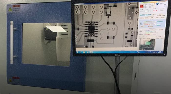
X-Ray inspection on PCBs begins by identifying the areas to be measured, such as joints, barrels, pads, and package features. The operator determines the projection, source energy, geometric magnification, field of view, and detector location that allow the intended target to be isolated with sufficient penetration through the material stack. The X-Ray program maintains a record of the target, imaging parameters, measurement area, criterion, and identification of the board, panel, or lot.
Once image processing is complete, the operator applies the approved area and calculation method. If features overlap, another angle, laminography, or CT must be used for analysis, while repeated signals across multiple boards require additional locations to be measured or lots to be analyzed.
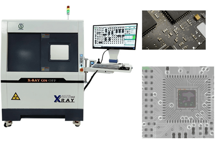
Inline AXI vs. Offline Analysis
Inline AXI is best suited for locations that require consistent verification during manufacturing, where the same packages, views, and measurement criteria are used continually, allowing quick feedback and location-based trending.
Offline analysis provides a more flexible analytical environment, where engineers may rotate the board, employ oblique views, use higher geometric magnification, focus on a selected layer, or reconstruct CT data at a selected site. Inline AXI first examines the defined locations, while unusual signals and complex overlaps are sent for offline analysis.
Hidden PCB Connections Requiring X-Ray Inspection
When a connection is inside a plated barrel, behind a shield, beneath a package, under overlapping material, or otherwise inaccessible to common inspection methods, X-Ray provides the primary imaging method for confirming its structural condition.

Bottom-Terminated Packages
BGA, LGA, and CSP packages hide their connection arrays under the component body. X-Ray visualizes ball-to-pad alignment, solder distribution, potential hidden bridges, missing connections, and solder collapse consistency.
For devices that use a QFN layout with a central thermal pad and perimeter terminations, the joints cannot be viewed optically after mounting. X-Ray delineates the pad region, indicates void distribution and solder coverage, and compares alignment with the placement footprint. Package guidance and the accepted measurement rule control acceptance.
FC and other fine-pitch connections have smaller bumps located beneath the die or package. X-Ray may assess bump placement, bump geometry, bridging, and density variation. Separating bump views from surrounding materials generally requires angled X-Ray projections or CT imaging.
Structures Beyond Optical Access
Although the PTH may appear acceptable from the surface, there could be internal voids or insufficient fill in the barrel. X-Ray identifies how solder flows through the barrel and distinguishes low fill from voided areas using a defined view and barrel reference. When an acceptance criterion is based on interface, plating features, or metallurgical information, a cross-section through the selected area determines acceptance.
Shields, tall components, and other supports can create an additional line-of-sight obstruction. Therefore, inspecting through the material stack to expose hidden terminations and connector regions requires more than simply increasing magnification. An angled beam, laminography, or CT imaging may be needed to achieve the separation required for acceptance.
AOI vs. X-Ray by Joint Visibility
AOI is generally used to view exposed leads, markings, and placement features. PCB X-Ray is used when the joint or barrel is hidden or when solder distribution through a barrel or thermal area must be measured. Electrical testing verifies continuity and operation. Cross-sectioning is used when interface, plating, or metallurgical evidence is required.
What Defects Can PCB X-Ray Inspection Detect?
Crack detectability is conditional on orientation, opening size, background contrast, material thickness, and overlap with other solder areas on the PCB.
| Defect or condition | X-Ray inspection role | Visible image signal | Possible process factors | Next confirmation or action |
|---|---|---|---|---|
| Suspected open connection | Strong structural support for joints beneath packages | Separation, missing solder path, incomplete collapse or abnormal joint geometry | Insufficient solder, non-wetting, HiP, displacement, damage or warpage | Electrical testing confirms the open state |
| Hidden solder bridge | Primary structural evidence when solder physically connects hidden joints | Dense solder path connecting adjacent pads, balls or leads | Excess paste, placement shift, collapse or reflow behavior | Mark the physical bridge; electrical testing confirms whether it creates a short |
| Suspected electrical short | Location evidence before the physical cause is confirmed | Abnormal dense path or conductive material near conductors or joints | Solder bridge, contamination, foreign material, alignment error or process variation | Electrical testing identifies the shorted nets; targeted imaging or inspection confirms the cause |
| Insufficient solder | Primary volume evidence for non-visible joints and PTH | Reduced solder mass, incomplete geometry or low barrel fill | Paste transfer loss, solder starvation, wetting or soldering setup | Use another view or cross-section when surface and barrel geometry remain ambiguous |
| Solder void | Primary internal-density evidence | Low-density region within solder mass; area, position and distribution are measurable | Flux volatilization, paste condition, pad design, thermal profile or trapped gas | Apply the approved denominator and segmentation method; correlate with material and reflow data |
| Excess solder | Primary hidden-volume evidence | Enlarged solder mass or excessive density around the joint | Paste overprint, stencil design, placement pressure or soldering variation | Check adjacent conductor spacing and bridge risk |
| Solder geometry consistency | Supporting process evidence | Variation in solder volume, shape, density or joint pattern across repeated locations | Combined material and process variation | Trend by location, panel and lot to separate recurring process drift from isolated variation |
| Hidden-array misalignment | Primary image evidence for concealed connection arrays | Ball-to-pad or package-shadow offset | Placement accuracy, board movement or reflow self-alignment variation | Measure against pad, package or centroid reference geometry |
| BGA short | Primary hidden-geometry evidence | Dense connection path between adjacent balls | Excess paste, ball collapse, placement offset or reflow variation | Electrical testing confirms the shorted connection; another angle resolves overlap |
| BGA open or HiP-like connection | Strong structural evidence | Separation line, waist, incomplete collapse, missing connection or abnormal ball geometry | Warpage, oxidation, paste transfer, placement or thermal mismatch | Repeat the same ball location at another angle; electrical testing or cross-section confirms the condition |
Solder Voids
Voids are defined as low-density areas within solder. A valid void percentage is based on the defined area of the joint or pad, using either a consistent contrast threshold, software segmentation method, or a documented manual-correction method. When voids are recorded using 2D, angled, laminographic, or CT imaging, the total area must not include unrelated top-side, bottom-side, or internal overlap. Superimposed features must not be counted as voids.
Results show isolated, clustered, interface-adjacent, or thermal-pad distributions. Although two different locations may have the same total void area, the resulting thermal or mechanical concerns differ based on those locations. The pattern of voids can help engineers determine where to focus paste, pad, material, or reflow evaluations. The same area, segmentation logic, and imaging method are used in both initial and repeat inspections for comparison.
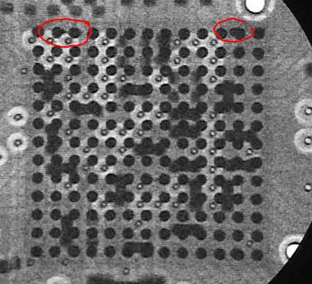
BGA Connection Defects
When diagnosing HiP defects, there is a risk of confusing natural ball necking, package shadow, or projection overlap with a true separation.
Oblique views or CT slices should reproduce the suspected interface at the exact same ball position before electrical continuity or a targeted cross-section confirms the separation. Misalignment is evaluated against the pad or package geometry rather than by using package shadow as a reference.
Microcrack Detectability
Microcracks may not become visible unless the plane and opening produce sufficient contrast along the beam path. A long, narrow crack nearly parallel to a single view may not be seen if dense copper or solder is nearby. Changing the viewing angle can increase contrast; CT can isolate the suspected plane, but voxel size and reconstruction artifacts still create uncertainty. Cross-sectioning remains the method of choice for the final determination of microcracks when metallurgical details or interface conditions control acceptance.
2D vs. 2.5D vs. 3D X-Ray Inspection
The correct inspection method depends on the ability to separate and measure the target features. The largest magnification number printed on a system specification is not the determining factor when choosing between these methods.
Inspection engineers begin with the least complex method that produces a stable result. Factors that affect the choice of method include target size, material density, thickness, field of view, required measurements, and production demand.
| Imaging mode | Image formation | Overlap handling | Primary inspection use | Production trade-off |
|---|---|---|---|---|
| 2D X-Ray | Single projection or real-time image | Top, bottom and internal features remain superimposed along the beam path | Routine screening of joints beneath packages, void pattern, alignment, solder volume and selected PTH checks | Lowest acquisition and processing demand when the target is readable in projection |
| Angled / oblique imaging | One or more off-axis projections | Changes the beam path to separate or expose a hidden feature | BGA interface analysis, PTH fill, shielded connections and dense local regions | Adds positioning and image analysis while avoiding full reconstruction |
| 2.5D X-Ray / laminography | Multiple angled projections or layer-focused reconstruction | Reduces overlap and separates selected depth planes | Double-sided boards, dense assemblies and selected interfaces | More acquisition and processing than 2D, less reconstruction than full CT |
| 3D X-Ray / CT | Multiple projections reconstructed into a volume | Isolates slices and separates complex internal structures | Failure analysis, complex PCBA, fine features and structures unreadable in projection | Highest acquisition, reconstruction and data-analysis demand |
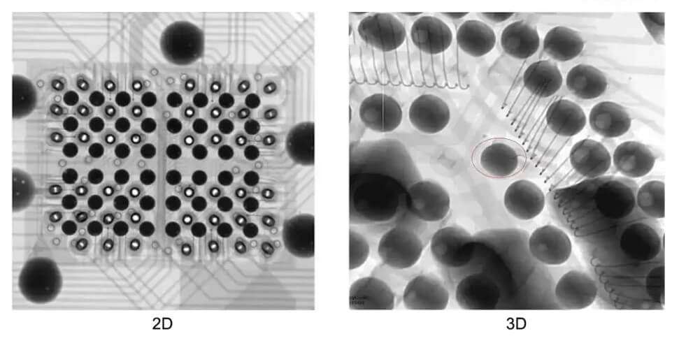
AXI is an automated system that implements an inspection process; it is not a separate type of X-Ray imaging geometry. A programmed AXI system can repeat supported 2D, oblique, or laminographic views at specific locations to screen production items, monitor trends, and give immediate process feedback.
2D X-Ray Inspection
2D X-Ray inspections have limitations because they provide only a two-dimensional projection, allowing no separation between different depths in the same projection. Unrelated features can make the 2D void percentage inaccurate when they enter the denominator or segmentation region. Either a different viewing direction or a method of separating features by depth must be used to provide the correct measurement.
2.5D Laminography
Oblique imaging causes the beam to pass through the sample at a different angle and therefore causes the interfering feature to move away from the target feature. SUGA configurations allow up to 82° of oblique viewing angle. The usable angle is determined by the size of the board, height of components, fixture clearance, and location of the target. Laminography can also use multiple angled images to focus on a specific depth band without reconstructing a full CT volume.
Laminography has a limited imaging angle range. Sample height limitations, sample motion during inspection, and interference from high-density material can create blurring in the target image even after the layers have been separated. Laminography is suitable for dense assemblies when the required feature remains repeatable under these constraints.
3D CT Inspection
CT requires more scanning, reconstruction, and data evaluation than 2D or laminography. The volume to be scanned, the size of the features, and the area being evaluated determine how the CT is set up. The larger the reconstructed volume, the less detail is available in the area of interest. When scanning high-density metals, the material can create streak artifacts or beam-hardening effects. Feature recognition, voxel size, and the ability to guarantee defect detection are not interchangeable terms; therefore, the feature of concern needs to be defined before scanning.
X-Ray System Capability and Usable Limits
| Capability field | Capability | What limits the usable capability |
|---|---|---|
| X-Ray source energy | SUGA X-Ray configurations provide source energy up to 160 kV for electronic assemblies requiring greater penetration | Select energy according to material thickness and density; do not present maximum kV as the default setting |
| Feature recognition | Submicron feature recognition is available on selected microfocus systems | Distinguish feature recognition from voxel size, nominal resolution and guaranteed defect detectability |
| Oblique viewing | SUGA X-Ray configurations provide oblique viewing up to 82° | Actual angle depends on board size, component height, fixture clearance and target location |
| Geometric magnification | Set through source-to-object and object-to-detector geometry | Maximum magnification does not guarantee usable contrast or sufficient field of view |
| Automated measurement | BGA, PTH, PoP and complex-package analysis can include automated pass/fail measurement and reporting | Use approved measurement regions and thresholds so initial and repeat inspection remain comparable |
| Low-dose inspection | ESD-safe handling and low-dose settings are available on selected systems for radiation-sensitive electronics | Exposure time, repeat scans and device sensitivity remain part of the exposure conditions |
| Rotation and positioning | Full rotational or multi-axis positioning is available where supported by the selected system | Mechanical access and board geometry determine usable motion |
The focal spot and detector response characteristics, together with object-to-detector and source-to-object distances, field of view, material stack, and contrast, create the geometric magnification trade-off between field of view, penetration, and visible detail. The established SUGA capabilities include a 160 kV source and an oblique viewing angle of up to 82°; the remaining functions are platform-dependent based on the inspection system selected and how the job is configured.
Double-Sided PCB Overlap
Double-sided PCBs may have components placed both above and below the target beam path. That means a top-side joint could overlap a component, shield, or internal copper region on the bottom side. The combined density of both areas could hide a void, merge a bridge, or distort the defined measurement region.
The engineer determines the target measurement and whether the 2D projection produces repeatable results. When structures cross the beam path, oblique imaging or laminography precedes full CT analysis. Source energy, projection geometry, field of view, and exposure follow the required penetration and feature recognition, while production quantity determines whether to use AXI or deeper offline analysis.
Which Requirements Control PCB X-Ray Results?
The customer drawing, contract, or approved specification identifies the features under customer control, product-specific limits, required inspection records, and customer overrides. An invoked standard provides the assembly, package, or sampling context; component guidance may define rules for how features must be measured. An approved inspection method establishes the view, region, segmentation method, calculation basis, coverage, and program version used to make the acceptance decision.
Package and Feature-Specific Rules
BGAs, QFN thermal pads, PTH barrels, and component arrays do not all have the same measurement region or reference geometry. Component or package-specific guidance determines when geometry or thermal requirements require a specific measurement rule. Marked images and measured results are accepted only against the rules invoked for each feature and method.
Standards and Sampling References
| Standard | Current revision | Technical role | Application in PCB X-Ray inspection |
|---|---|---|---|
| IPC-A-610 | Revision J, released 2024 | Post-assembly acceptability context for electronic assemblies | Use with the customer-invoked class and applicable feature requirement |
| IPC J-STD-001 | Revision J, released 2024 | Requirements for soldered electrical and electronic assemblies, including process and acceptance context | Explain together with IPC-A-610J rather than treating either document as a universal X-Ray threshold table |
| IPC-7095 | Revision E, released 2024 | Design, assembly, inspection, repair and reliability guidance for BGA and FBGA packages | Use for BGA-specific geometry, inspection planning and anomaly analysis |
| IPC-7093 | Revision A, released 2020 | Design and assembly guidance for bottom-termination components such as QFN, DFN, SON and LGA | Use for BTC-specific design, inspection, repair, quality and reliability guidance |
| ISO 2859-1 | Edition 3, 2026 | AQL-indexed lot-by-lot attribute sampling when statistical sampling is appropriate and approved | Do not use as a defect acceptance limit; use only to define a sampling plan |
Feature-Specific Measurement Criteria
A percentage or offset becomes useful only after the object, region, method, and calculation basis are defined.
| Inspected feature | Measurement object | Required measurement basis | Controlling requirement | Reported result |
|---|---|---|---|---|
| Individual BGA ball void | Void area within one solder ball | Ball region, segmentation method, projection overlap and selected view | Customer requirement, IPC-7095E context, approved package or inspection rule | Ball location, void value, method and result |
| Cumulative BGA void distribution | Combined void pattern across a defined ball, row or package region | Aggregation method, locations included and calculation basis | Approved project or package criterion | Measurement set and package-level result |
| QFN/BTC thermal-pad void | Void area and distribution within the defined thermal pad | Pad region, segmentation, interface location and thermal-pad design | Customer requirement, IPC-7093A context and component guidance | Marked pad image, value, distribution and result |
| Solder bridge | Unintended connection between adjacent conductors | Image view, connected features and hidden/visible location | Customer requirement and applicable assembly acceptance rule | Marked bridge location and final action |
| Insufficient solder or PTH fill | Solder coverage, fill distribution or barrel geometry | Termination type, measurement view, barrel reference and applicable area | Customer requirement, J-STD-001J / IPC-A-610J context and approved method | Fill or coverage measurement and result |
| Component or array misalignment | Offset between component, ball, termination and pad geometry | Reference edges, centroid or electrode geometry and allowed direction | Customer drawing, package guidance and applicable acceptance requirement | Offset measurement, direction and result |
The initial and repeat inspections use the same measurement basis. For voids, this means using the same denominator and segmentation logic. For fill, coverage, and alignment, this means using the same view and reference geometry.
How Is the Final Result Decided?
The final result is determined by comparing the measured feature with the controlling requirement using the approved view and calculation basis. If the image evidence remains ambiguous, the next step is to take another view, conduct an electrical test, take a selected cross-section, verify the rework, or reject the feature.
ISO 2859-1:2026 may define an approved AQL-indexed lot sampling plan, but it does not define the engineering limit for a solder defect.
X-Ray Inspection Deliverables
The deliverables associated with X-Ray inspection include a package that identifies the inspected PCB, panel, or lot; target locations; imaging method and configuration; original and marked images; measured values, units, regions, and calculation basis; the controlling customer, standard, or package requirement; and the final result or action. The program version, equipment used, and calibration records maintained as part of the completed inspection preserve traceability for future inspections.
How Is Inspection Coverage Set?
| Coverage type | Appropriate use | Required definition | Follow-up action |
|---|---|---|---|
| 100% inspection of defined locations | Critical packages, first article, process introduction, high-risk joints or customer-required coverage | Exact boards, locations and sites per board | Repeat or broaden views when a location cannot be measured consistently |
| Approved lot sampling | Stable production where statistical attribute sampling is appropriate | Lot definition, ISO 2859-1:2026 or customer-approved sampling plan, AQL and inspection level where applicable | Expand coverage when a critical, repeated or pattern-based finding appears |
| Periodic process monitoring | Ongoing trend control after the inspection program is established | Frequency, target locations, measurement method and trend limits | Assess printing, placement, reflow or soldering data when a trend changes |
| Focused engineering analysis | Selected failed units, unusual image signals or complex structures | Unit identity, target, method and comparison sample | Add angled, CT, electrical or cross-section evidence according to the question |
How Are X-Ray Results Traced?
Each result links those identifiers to the board or lot, inspected location, program version, equipment record, view, measurement region, and calculation basis. Repeat inspection reuses the same identifiers and settings; if the original projection is unstable, the report records the added oblique, laminographic, or CT method instead of comparing unlike measurements.
How Do X-Ray Findings Guide Process Changes?
BGA separation, alignment, or collapse patterns can indicate issues with placement, package warpage, paste transfer, or reflow. The pattern of voids formed beneath QFN or BTC thermal pads can indicate process-related issues with the stencil, paste, pad design, or thermal profile. PTH fill trends can indicate wave- or selective-solder parameters and local thermal mass.
Teams categorize defect patterns by location, panel position, lot number, reflow lane, or assembly line. Following a process adjustment, teams re-inspect using the same method and measurement region used before the adjustment. The data collected from X-Ray inspection is correlated with the corresponding print, placement, reflow, material, and electrical data to establish the root cause.
X-Ray Inspection Applications

Aerospace and Defense Electronics
Dense or double-sided assemblies may place BGA, bottom-termination, fine-pitch, and PTH connections behind shields or overlapping metal. SUGA may document the overlap and feature size using 2D, oblique, laminographic, or CT images, but the specific location and method must be documented precisely. After rework, the same geometry is applied again. If projection cannot separate an interface, CT scans or an appropriate cross-section are needed.

Automotive Electronics
Automotive controller, sensor, power, and interface PCBAs often use high-volume AXI screening followed by offline analysis of BGAs, QFNs, hidden bridges, and selected PTH fill. Any defect found during AXI screening must be resolved before production can continue. Once a signal is found during screening, the true defect must be distinguished from false signals caused by component shadowing, panel position, or normal production geometry. Location and lot trends direct stencil, paste, placement, reflow, wave, or selective-solder evaluation. A critical or repeated finding can expand coverage from sampling to 100% inspection at named sites, and reworked boards are measured with the same region and calculation basis.

Medical Devices
Because medical PCBAs contain critical solder joints that are hidden and difficult to detect optically, the engineer must determine which areas of the assembly require X-Ray inspection by reviewing the product risk analysis files and customer requirements. Depending on a part's design and condition, an engineer may use 2D, oblique, laminographic, or CT imaging to determine whether a defect is present and link the marked images and measurements to the serial number or lot during production. Repeat inspection must use the same region and imaging method. The critical locations and limits come from the product risk file, customer requirement, or approved specification rather than a universal void percentage. Devices with a supplier-specified radiation limit require controlled exposure and documented scan conditions.

Industrial Automation
Defects such as solder voids beneath power-component thermal pads, low PTH fill in high-thermal-mass connectors, solder beneath relays or modules, and hidden terminations are typically detected by X-Ray inspection. In some cases, low PTH fill, internal voiding, projection overlap, and high connector mass can appear similar in a 2D view. Using oblique imaging or laminography changes the X-Ray beam orientation and can provide a clearer view. CT scans or cross-sections may further verify a suspected interface. During X-Ray inspection, solder volume and soldering-process conditions can be assessed; however, relay operation, isolation, analog accuracy, and load performance are verified by electrical or functional testing.
Power Electronics and Energy Storage
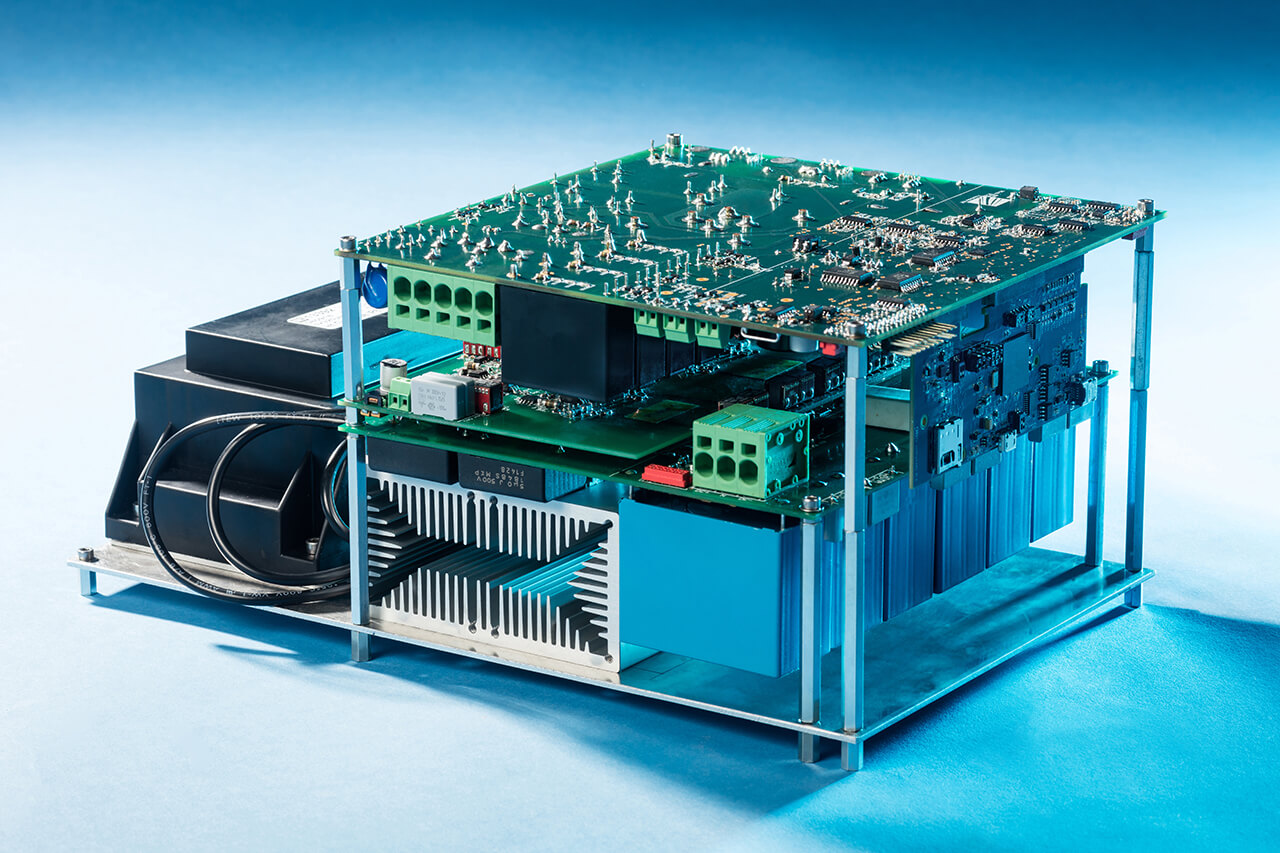
Power PCBAs typically consist of thick copper, bus structures, shields, large thermal pads, and hidden high-current connections. When measuring solder volume and solder voids beneath MOSFETs, IGBTs, power modules, and large thermal pads, the X-Ray measurement region must exclude unrelated metal and overlapping solder structures from the thermal-pad denominator. Solder voids are evaluated by both their location and overall area. X-Ray also checks PTH fill at bus or high-current connectors.
When multiple voids or overlapping solder features are suspected, higher-energy beams, oblique views, laminography, or CT may be required to determine whether separate features are present. While voids and solder volume may be assessed as part of the soldering process, powered testing verifies voltage and current regulation, temperature rise, protection, and electrical characteristics under load.

Consumer Electronics
Selective PCBA X-Ray inspection or AXI screens small BGA, CSP, QFN, PoP, and fine-pitch joints that cannot be accessed after assembly. Programmed locations use the fastest stable view for screening. Selected findings move to oblique imaging, laminography, or CT when the 2D view cannot separate the target. PoP stacks, double-sided placement, batteries, shields, and dense internal copper can create overlap that increases false calls or changes apparent void area.

Telecommunications
Telecommunication PCBAs are large, double-sided, and high-density, with dense BGA arrays, shielded RF or control areas, high-pin-count connectors, magnetic components, and multilayer overlap. As a result, these features may overlap and prevent a single projection from separating the target. Angled X-Ray images may help identify hidden bridges, void patterns, alignment issues, and connection geometry. X-Ray does not determine impedance, insertion loss, eye quality, bit-error rate, or successful link establishment. Signal-integrity, boundary-scan, or functional communication testing is required to confirm these specifications.

IoT Devices
The assembly of IoT devices uses compact LGA, CSP, QFN, BGA, wireless-module, and gateway connections. Module-to-board joints may overlap the module substrate or opposite-side components, while an installed shield may limit the available beam angle.
SUGA chooses to conduct inspection before or after shield installation based on the connection targeted during inspection. SUGA applies oblique imaging or CT only when the targeted 2D view cannot separate the structure.
X-Ray provides physical evidence of solder distribution, alignment, bridges, and solder connection formation. RF performance, antenna behavior, sensor response, or final device operation requires electrical or functional testing. Battery, MEMS, or sensor supplier exposure limits also apply when specified.
Our PCBA Production Lines
















PCB X-Ray Inspection FAQ
X-Ray can identify structural conditions associated with an open connection, including missing solder, incomplete collapse, separation, and misalignment. It does not measure net continuity. Electrical testing confirms whether the circuit is open.
When components, shields, copper structures, or package layers overlap the target, 2D X-Ray may not provide enough detail for the measurement. Reconstructed slices or volumes can distinguish interfaces and separate complex internal geometry. When the target remains distinct, 2D X-Ray provides faster acquisition and requires less data processing.
No. Factors that determine BGA coverage include package geometry, product risk, process maturity, customer requirements, electrical access, and available inspection evidence. First articles, new packages, critical arrays, and repeated defect patterns may require 100% inspection at specified locations. Stable production can use sampling or periodic monitoring according to the approved coverage.
Only if the denominator, segmentation method, view, geometric configuration, and overlap handling are equivalent. A 2D projection, oblique image, laminographic layer, and CT slice can produce different apparent areas because they separate structures differently. A void report should include the measurement method and region. Trend data should compare like-for-like measurements rather than combine percentages from different image geometries.
Routine PCB X-Ray inspection is non-destructive for standard assembly inspection, but cumulative exposure and repeated scans matter for sensitive semiconductor components. Exposure time and repeated scans should be limited to what is needed to obtain the required image. Supplier radiation limits should be followed when specified. Suspected radiation-related effects should be confirmed by electrical or functional testing.