Upload BOM & Gerber
-
Mobile: +86 13312967631
-
Email: sales@sugaintl.com

PCB Assembly Services
OEM and Custom PCBA Manufacturer in China
Full and partial turnkey PCB assembly from China, covering PCB fabrication, component sourcing, SMT and through-hole assembly, inspection, testing, programming, and product-level integration.
3–5 Days
Prototype Assembly
01005
Fine-Pitch Placement
1–40 Layers
PCB Capability
99.6%
On-Time Delivery
What Is PCB Assembly?
PCBA refers to the process of assembling or putting together a PCB with components, as well as conducting tests, inspections, and creating records of the assembly. The assembly process takes a bare PCB that has no electronic components installed through final assembly. A finished bare PCB is not yet a working electronic assembly; it provides the copper paths, pads, holes, and mechanical structure. Assembly adds the components, solder joints, inspection records, and agreed test work that make the board usable in a product.
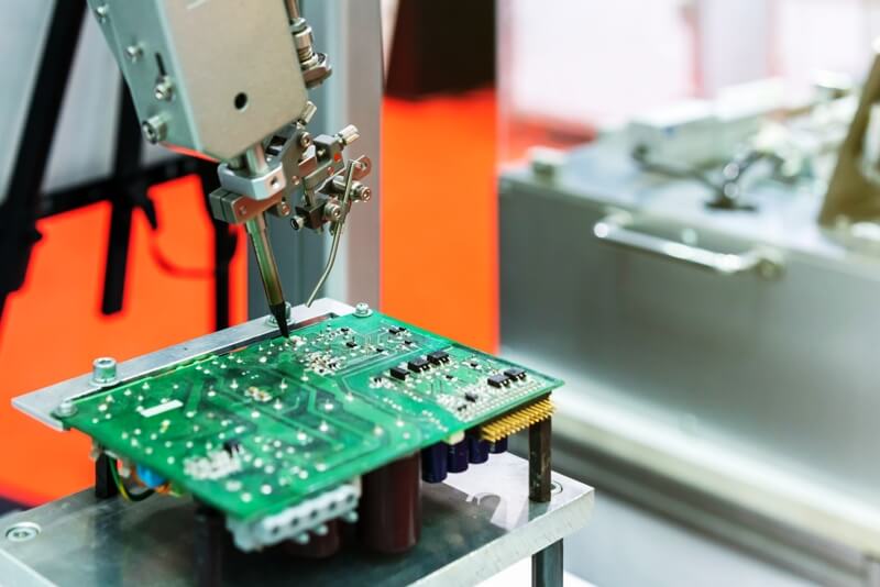
PCB vs. PCBA
First, the difference between a populated PCB and an unpopulated PCB is whether electronic components are installed on the PCB. Second, while a PCB has only the electrical connections for its components, a PCBA includes both the electrical connections and the installed components that create an assembly.
PCBAs include not only the electrical connections between components but also their connections to the PCB. Also, since all of the components are connected to the PCB, the components must be installed onto the PCB using soldering techniques, and the solder joints must be checked for defects.
What Do PCB Assembly Services Deliver?
Customers can send us their PCB designs and the required documentation, and we will build PCB assemblies for them using the specified materials. The completed delivery is a populated PCBA with the agreed inspection and test work finished. Production can begin with PCB fabrication and component sourcing or with customer-supplied boards and parts.
Our Services
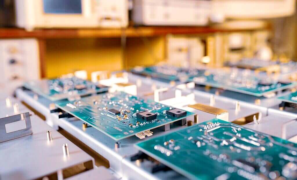
Full Turnkey PCB Assembly Services
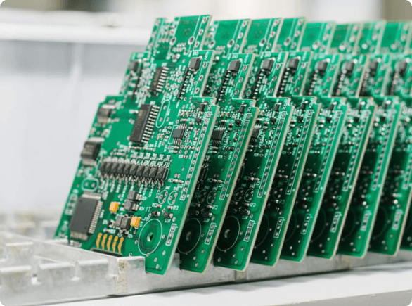
Prototype PCB Assembly Services
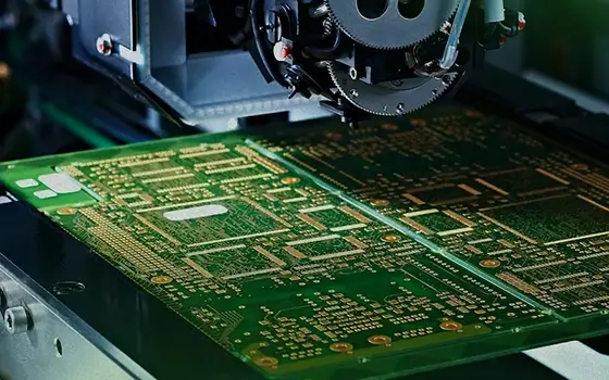
Quick Turn PCB Assembly Services
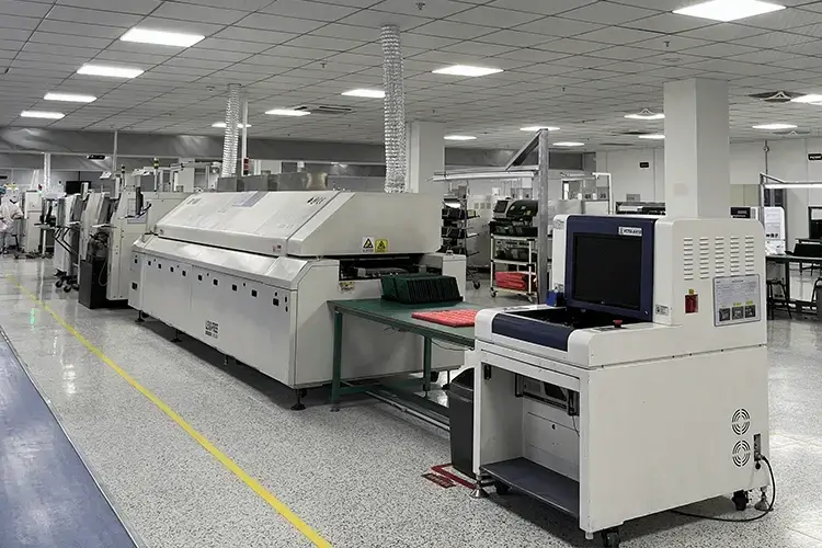
SMT PCB Assembly Services
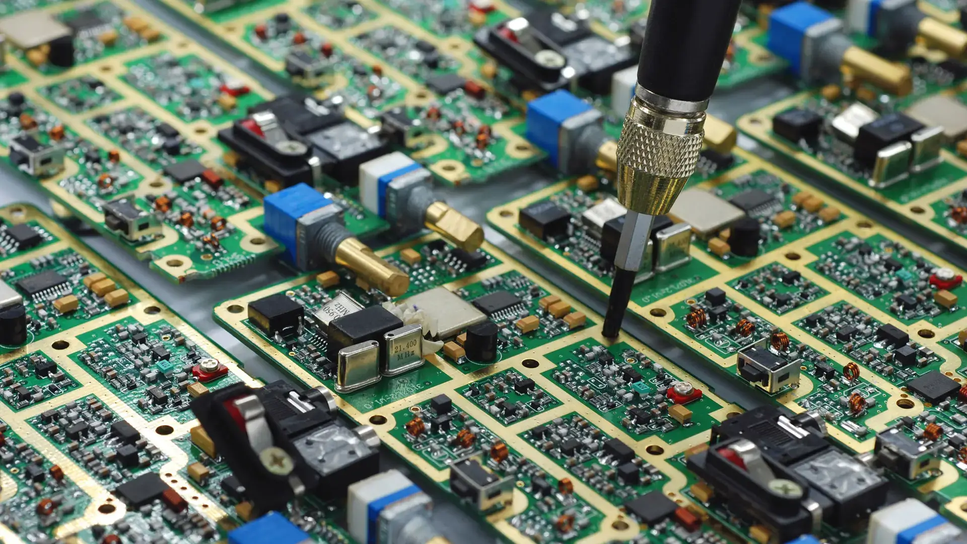
Through-Hole PCB Assembly Services
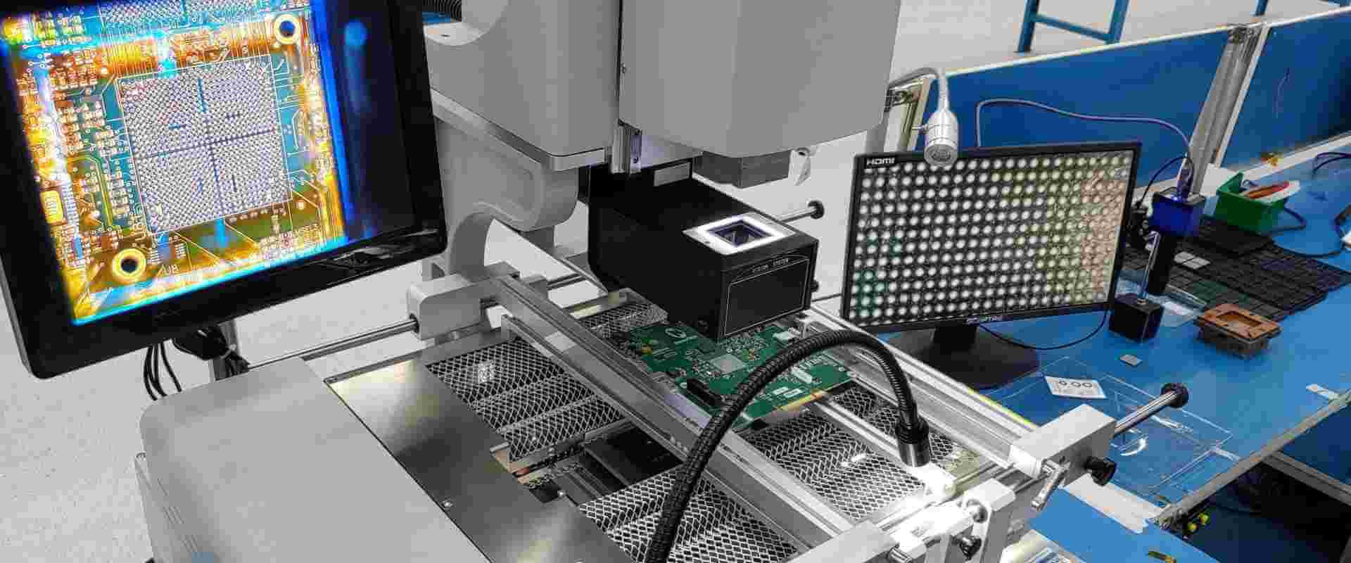
BGA Assembly Services
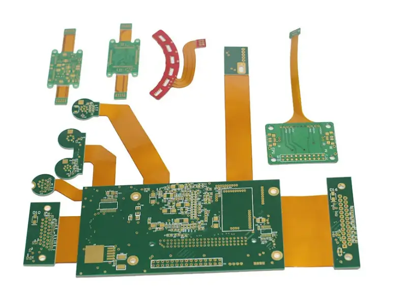
Flex & Rigid-Flex Assembly Services
Low Volume PCB Assembly Services
High Volume PCB Assembly Services
Consigned PCB Assembly Services
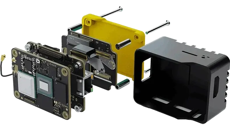
PCB Box Build Assembly Services
Lead-Free PCB Assembly Services
PCB Assembly Service Models
The assembly model will define the source of the PCB, components, and materials that are included in the assembly kit. An assembly service may use a combination of commercially purchased parts, ICs owned by the customer, PCBs supplied by the customer, and components that are already in the customer’s possession. SUGA’s controls for each of the project categories are as follows:
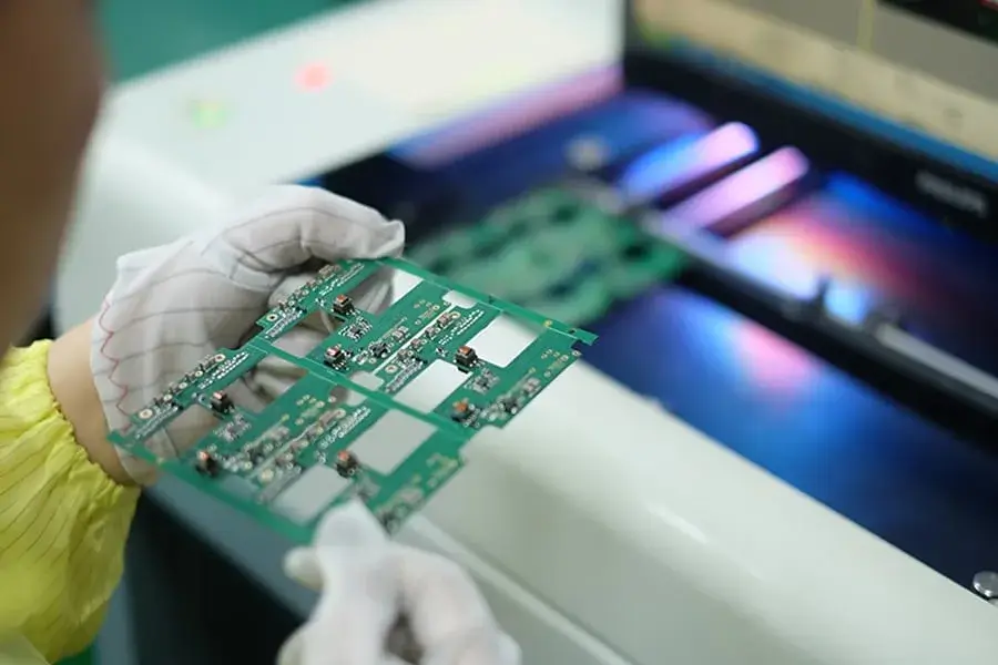
| Service Model | Customer Controls | SUGA Controls | Best Fit |
|---|---|---|---|
| Full Turnkey PCB Assembly | Approved Gerber, BOM, placement data, test requirements | PCB fabrication, all component sourcing, assembly, inspection, testing, packaging | Projects requiring one supplier to manage the complete PCBA delivery |
| Partial Turnkey PCB Assembly | Critical ICs, controlled parts, long-lead parts, or existing inventory | PCB, remaining components, assembly, inspection, testing | Projects where selected parts remain under customer control |
| Consigned PCB Assembly | All or most PCBs and components | Incoming inspection, kitting, assembly, inspection, testing | Projects requiring customer-controlled MPN, lot, date code, or source |
| Kitted Assembly | Complete material kit prepared by production batch | Kit verification, shortage check, assembly, testing | Projects with an existing purchasing or inventory team |
For full turnkey projects, authorized or traceable channels such as Digi-Key, Mouser, Arrow, Avnet, Newark, and Element14 support component availability and traceability. Each part supplied by the customer for a partial turnkey project requires a specified MPN, package, voltage or current rating, temperature grade, and approval status.
Consigned PCB Assembly
Materials received for consigned PCB assemblies may come as bare boards, full reels, cut tape, trays, tubes, loose parts, or bulk through-hole components. During incoming inspection, MPNs, packages, labels, date codes, moisture status, visible condition, and solderability of the materials are verified before kitting.
Kitted Assembly
For projects where a complete material kit has been prepared, SUGA verifies that the kit includes the parts listed on the BOM, checks that the quantities and package presentation match, identifies any shortages, and prepares the materials for assembly and testing.
How Are Component Substitutions Controlled?
Sourcing decisions are based on an exact MPN instead of terms like “in stock equivalent.” An acceptable substitution must match the footprint, package, electrical rating, temperature grade, and lifecycle requirements of the MPN being substituted.
Traceable sourcing, multi-supplier availability searches, cross-referencing, and lifecycle checks are used to support projects containing rare, obsolete, or allocation-sensitive components. For repeat production, tracking MPNs, lots, date codes, and lifecycle status supports inventory management and the preparation of a stable approved-alternative list.
Availability does not equate to approval. No substitution will enter production without prior written approval confirming the electrical, mechanical, and lifecycle compatibility of the substitute with the end-product design.
PCB And Assembly Capabilities
The assembly method and production configuration are determined by the number of layers on the board, the physical construction of the board, the component package geometry, component presentation, panel design, and inspection access.
| Capability | SUGA Service Range |
|---|---|
| PCB Layers | 1–40 layers |
| PCB Types | Rigid PCB · Flexible PCB · Rigid-Flex PCB · HDI · Impedance-Controlled PCB |
| Board Thickness | 0.5–4.5 mm |
| Minimum Trace / Space | 2.0 / 2.0 mil |
| Minimum Mechanical Hole | 0.2 mm |
| Controlled Impedance | ±5% |
| Copper Weight | Standard copper to 10 oz heavy copper |
| Assembly Sides | Single-sided · Double-sided |
| Assembly Types | SMT · Through-Hole · Mixed SMT + THT |
| Order Quantity | From 1-piece prototypes to 10,000+ board production lots |
| Smallest Component | 0201 metric class (0.25 × 0.125 mm) |
| Common Fine Components | 0201 · 0402 · 0603 imperial sizes |
| Package Support | SOIC · DFN · QFN · QFP · BGA · uBGA · LGA · CSP · CGA · PoP · Flip-Chip · PLCC |
| Minimum BGA Ball Pitch | 0.2 mm |
| Minimum BGA Ball Diameter | 0.14 mm |
| Minimum QFP Lead Width | 0.15 mm |
| Placement Accuracy | ±30 μm @ 3σ |
| SMT Placement Speed | Up to 60,000 components/hour |
| SMT Production Scale | 3–4 million solder pads/day |
| Through-Hole Capacity | Up to 100,000 pins/day |
| Individual PCB Size | Down to approximately 5 × 5 mm with suitable panelization |
| Assembly Panel Size | Up to 610 × 508 mm |
| Component Packaging | Reel · Cut tape · Tray · Tube · Loose parts · Bulk |
| SMT Soldering | Lead-free reflow · Leaded reflow · Nitrogen reflow · Custom profile |
| Through-Hole Soldering | Wave soldering · Selective soldering · Precision hand soldering |
| PCB Surface Finish | ENIG · HASL · OSP · Immersion Silver · Immersion Tin |
| PCB Features | Blind/buried vias · Microvias · Via-in-pad · Resin-filled vias · Castellated holes · Edge plating |
| Assembly Workmanship | IPC-A-610J Class 2 / Class 3 |
| Soldering Process | IPC J-STD-001J |
| Environmental Compliance | RoHS 2011/65/EU amended by (EU) 2015/863 · REACH SVHC screening against the current Candidate List |
| Inspection Coverage | IQC · FAI · 3D SPI · 2D/3D AOI · X-Ray |
| Electrical/Test Coverage | Flying Probe · ICT · FCT · Open/Short · Custom Functional Test |
PCB Fabrication and Component Package Range
A board around 5 × 5 mm can be assembled when panelization, process rails, and fiducials allow the printing, placement, and depaneling equipment to handle the individual CBA stably. Often, small CBAs are designed with breakaway rails, tooling holes, or a carrier to ensure that the individual outline of each CBA is not used as the handling surface. The 610 × 508 mm figure describes the maximum assembly-panel size, while individual circuit board size depends on the features associated with panel design and handling.
Dense fine-pitch and array package types will require the PCB assembly and reflow process to be developed based on the CBA design.

SMT, Through-Hole or Mixed Assembly?
Product assembly methods depend on the physical requirements of the product. Different assembly processes are required for compact communications boards, power supplies utilizing heavy connectors, and industrial controllers with dense logic and high-power hardware. The assembly method will affect the CBA layout, fixture planning, thermal exposure, repair methods, and line setup.
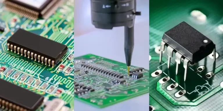
Surface Mount Assembly
Best fit: Compact boards, high-I/O packages, dense consumer, IoT, and communications products.
Main strength: High-density assemblies, double-sided placement, and short interconnect paths.
Main production control: Stencil design, paste printing, placement accuracy, and reflow profiles.
Through-Hole Assembly
Best fit: Connectors, terminals, transformers, large capacitors, high-current parts, and mechanically stressed components.
Main strength: Excellent mechanical retention, component repairability, and support for large components.
Main production control: Hole fit, lead length, wave soldering, and solder fill.
Mixed Technology Assembly
Best fit: Power supplies, industrial controllers, automotive control boards, and communications equipment.
Main strength: High-density SMT logic combined with robust THT power and connector sections.
Main production control: Process order, thermal protection, fixture clearance, and selective soldering.
Normally, SMT-side placement and reflow are carried out before through-hole component insertion and soldering. When performing SMT operations on both sides of the board plus through-hole work, it is necessary to determine which components are to be soldered on the second side, what type of carrier is to be used, how much clearance is needed for the fixture, and which areas of the board are acceptable for selective soldering. The insertion sequence for large connectors, transformers, and heat-sensitive parts may need to be separate.
Which Files Define the Assembly?
Every file must identify the same board revision, reference designators, component intent, mechanical features, and acceptance conditions. A complete BOM cannot make up for an obsolete placement file, nor can a complete Gerber package correct the orientation of an unmarked connector. File names are not sufficient to enforce revision control because exported drawings, centroid files, and Gerber archives can be generated at different times.
| File / Data | Required Content | Supported Formats / Examples | Used By |
|---|---|---|---|
| PCB Fabrication Data | Layers, outline, drill, copper, solder mask, silkscreen | Gerber RS-274X, ODB++, .gbr, .cam, .brd, .pcbdoc | PCB fabrication and DFM |
| Bill Of Materials | Reference designator, value, quantity, package, MPN, manufacturer, DNP status | .xls, .xlsx, .csv | Purchasing, IQC, kitting |
| Pick-And-Place Data | X/Y coordinate, rotation, side, reference designator, package | Centroid, XY, ASCII, .txt, .csv | SMT programming |
| Assembly Drawing | Polarity, orientation, connector direction, special placement notes | PDF, drawing export | FAI, manual assembly, inspection |
| Panel Drawing | Panel size, rails, fiducials, tooling holes, V-score/routing | Gerber, PDF | Stencil, printing, depaneling |
| Programming Files | Firmware, device type, version, checksum, interface, programming stage | HEX, BIN, customer instruction | IC programming |
| Test Instructions | Test points, power input, limits, fixtures, software, pass/fail criteria | PDF, spreadsheet, software package | ICT, FCT, functional test |
| Packaging And Label Data | Label text, serial number, barcode, ESD and moisture requirements | PDF, spreadsheet | Final packaging |
PCB Assembly Process
How Are Boards and Components Prepared?
Preparation of the components to be assembled onto the board begins with checking the Gerber files, BOM files, placement data, and assembly drawing files for consistency. DFM/DFA reviews verify the footprints, polarity, clearances, panel design, fiducials, and test points, in addition to listing any approved alternatives and the test plan before the production files are released.
PCB fabrication and component sourcing can occur concurrently. PCB preparation consists of evaluating the appearance, dimensions, and surface finish and confirming the warpage and electrical characteristics of the PCB so that proper printing, placement, reflow, and fixture contact can be achieved.
The components received from the supplier must also be checked against the BOM and production data for MPN, value, package type, quantity, date code, MSL, label, and physical condition. Kitting allows missing materials to be detected before they are used on the production line, while packaging form dictates feeder setup, polarity confirmation, label handling, and manual preparation for parts that cannot be loaded into the feeder automatically.
The MSL and floor life of moisture-sensitive parts are tracked. Baking and dry storage minimize moisture-related cracking, delamination, and reflow defects. The material record contains the MSL and floor-life status, as well as the baking and dry-storage conditions before placement on PCBAs.
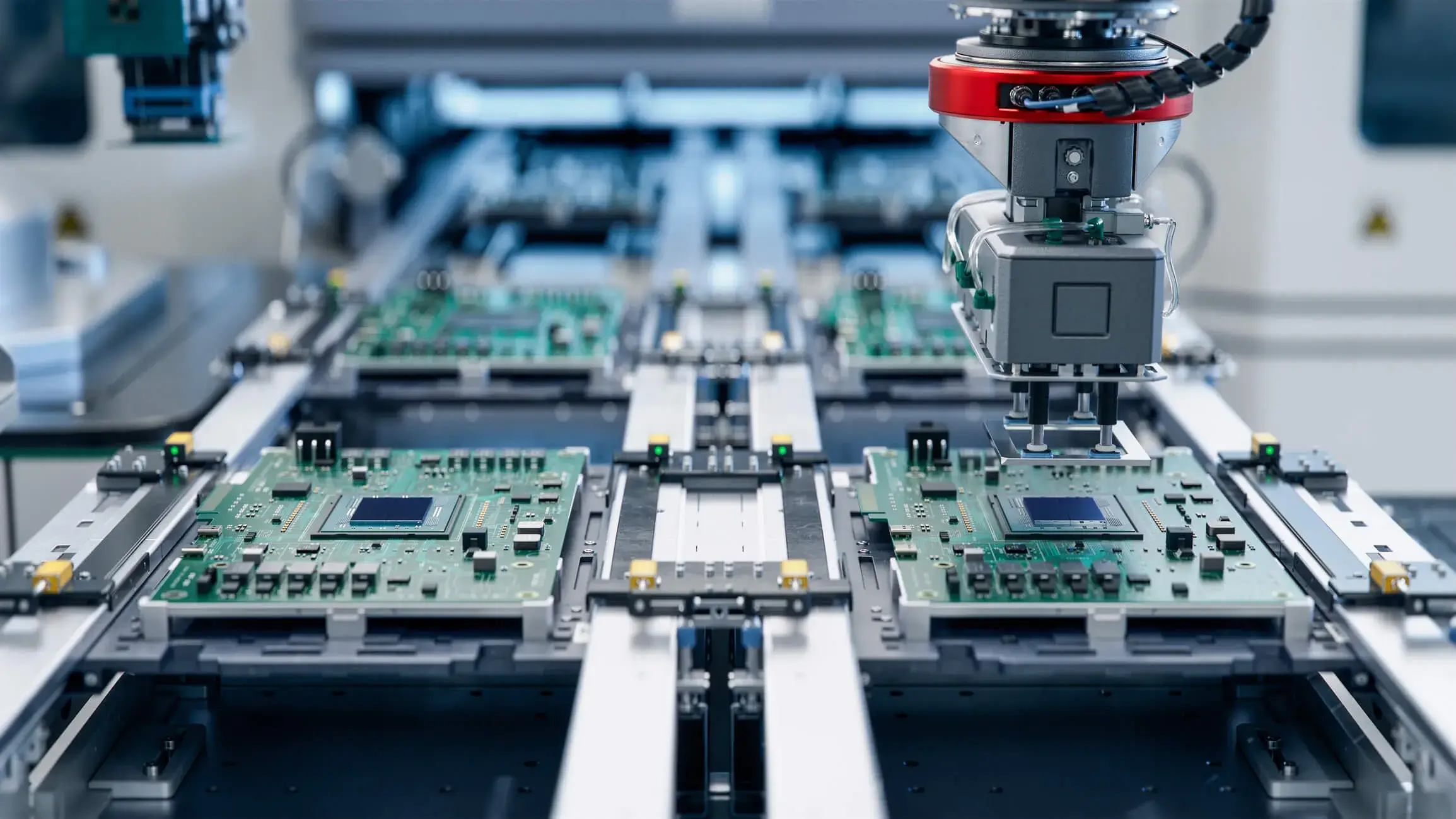
Stencil Design for Stable Paste Printing
Stencil selection affects how solder paste is printed before placement. Stencils designed using standard criteria are used with conventional solder-paste deposit patterns. In contrast, step stencils can be used on boards that combine fine-pitch pads with large pads requiring different solder-paste volumes. Nano-coated stencils improve the release of paste from small apertures.
Stencil design, unpopulated pads, stencil thickness, and aperture balance influence the volume of solder paste used and the risk of components being tombstoned. Paste is properly stored, thawed, and mixed before printing, and stencil alignment, squeegee pressure, and print speed are verified during print setup. 3D SPI confirms that the solder paste deposited on the pads meets the assembly specifications. Low- to mid-temperature solder paste options are available for assemblies that require different thermal profiles.
How Are SMT and Through-Hole Processes Sequenced?
SMT assembly is composed of solder paste printing, feeder setup, component verification, pick-and-place machine programming, and first-piece placement checks. Particular attention must be paid to ensure that components on both sides are properly positioned and that polarity and pin-1 orientation are correct for parts that cannot be corrected through reflow.
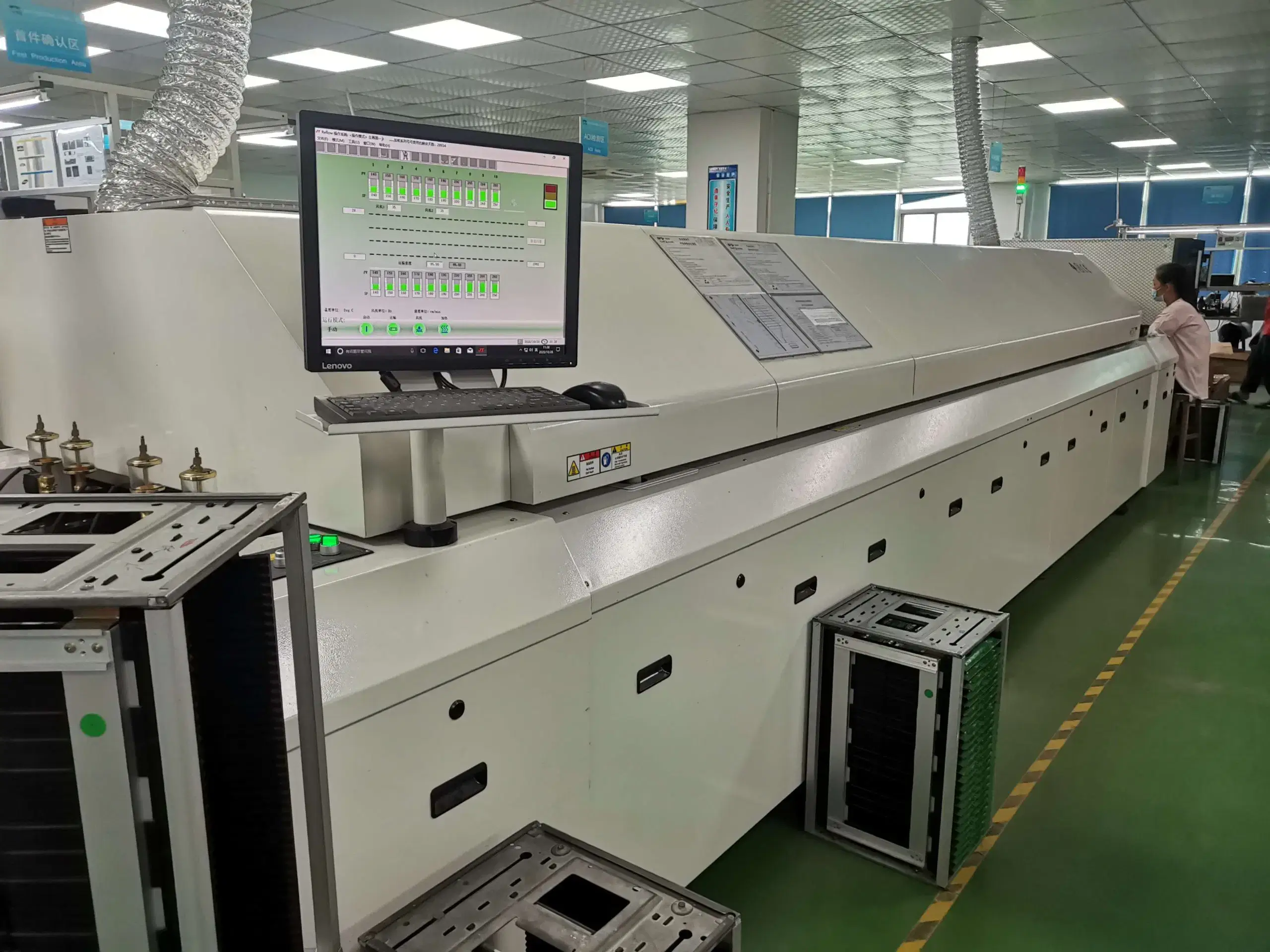
During the reflow process, the board passes through preheat, soak, peak, and cooling zones, typically using a defined lead-free or leaded profile, with nitrogen where required, based on the assembly being produced. The resulting board is classified as a reflowed SMT assembly.
The addition of axial and radial components, along with connectors, terminals, transformers, relays, and other large assembly components through automatic or manual insertion, is used to manufacture through-hole and mixed-technology PCBAs. Wave soldering, selective soldering, or precision hand soldering is selected based on the required fixture clearance and thermal protection, and the resulting product is a fully populated PCBA.
How Are Boards Programmed and Tested?
Programming of boards takes place either before placement or after assembly has been completed. The programming record gives the firmware version, checksum, and serial number associated with each programming stage and identifies the programming interface, such as JTAG, SWD, UART, or a custom interface.
For products that use a golden sample, external loads, communication interfaces, or test fixtures to validate that a board is functional, the same setup is used to reproduce the pass condition during testing. Checks of the board label, barcode, serial number, workmanship quality, and test reports confirm the final condition of the board.
What Production Records Are Available?
Traceability records include identification of the PCB lots and component lots received, component date codes, incoming inspection results, feeder and placement programs for each component, solder-paste lot number, stencil used for the assembly, reflow profile used during manufacturing, SPI and AOI history, X-ray results where applicable, rework, scrap, line yield, and production status.
First-article inspection results and fixture or software versions may be maintained with the documentation for the specific test method used for the assembly. The types of records available depend on the project requirements and the documentation required with delivery of the finished product.
PCB Assembly Inspection And Testing
Different types of defects manifest at different stages and locations. Incoming inspection cannot verify reflow-joint quality, nor can an X-ray photograph determine whether the board is functional or communicates appropriately. Therefore, each inspection method and production stage has a specific verification target.
| Method | Main Purpose | Finds / Verifies | Best Used For |
|---|---|---|---|
| IQC | Verify incoming PCB and components | Wrong MPN, package mismatch, damage, moisture status, PCB defects | Every material lot |
| FAI | Confirm first assembled board | Placement, polarity, BOM match, assembly drawing match | Prototype, NPI, new revision |
| 3D SPI | Measure solder-paste volume, height, area, and offset | Insufficient paste, excess paste, printing offset, uneven deposition | SMT before placement |
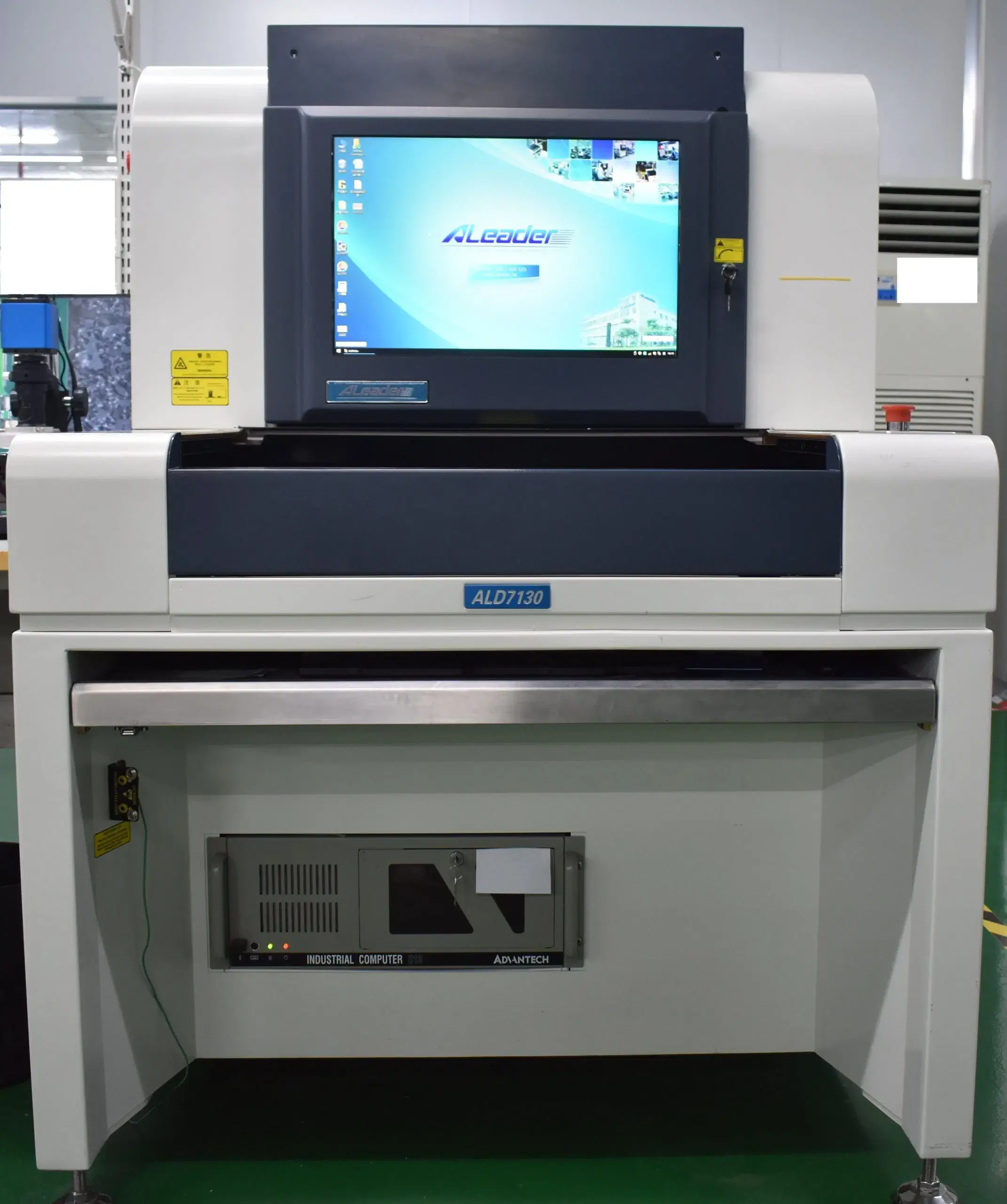
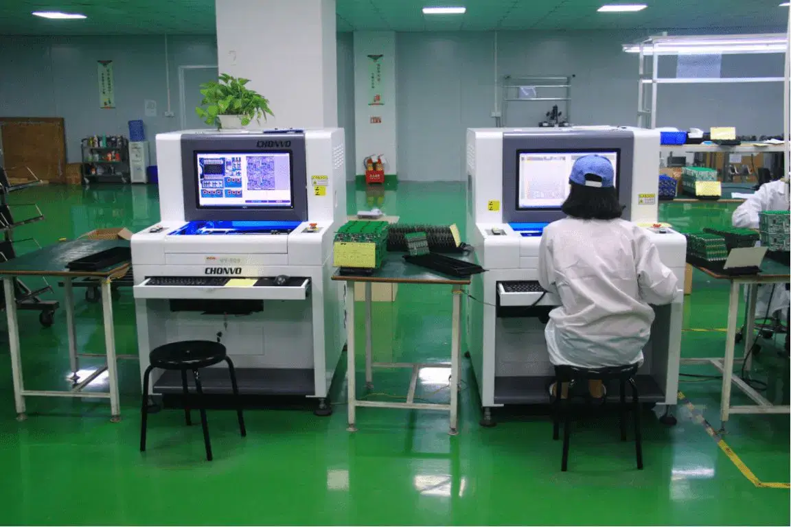
| 2D / 3D AOI | Inspect visible components, solder joints, and component height | Missing or wrong parts, polarity, misalignment, lifted leads, bridging, visible solder defects | SMT production |
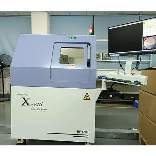
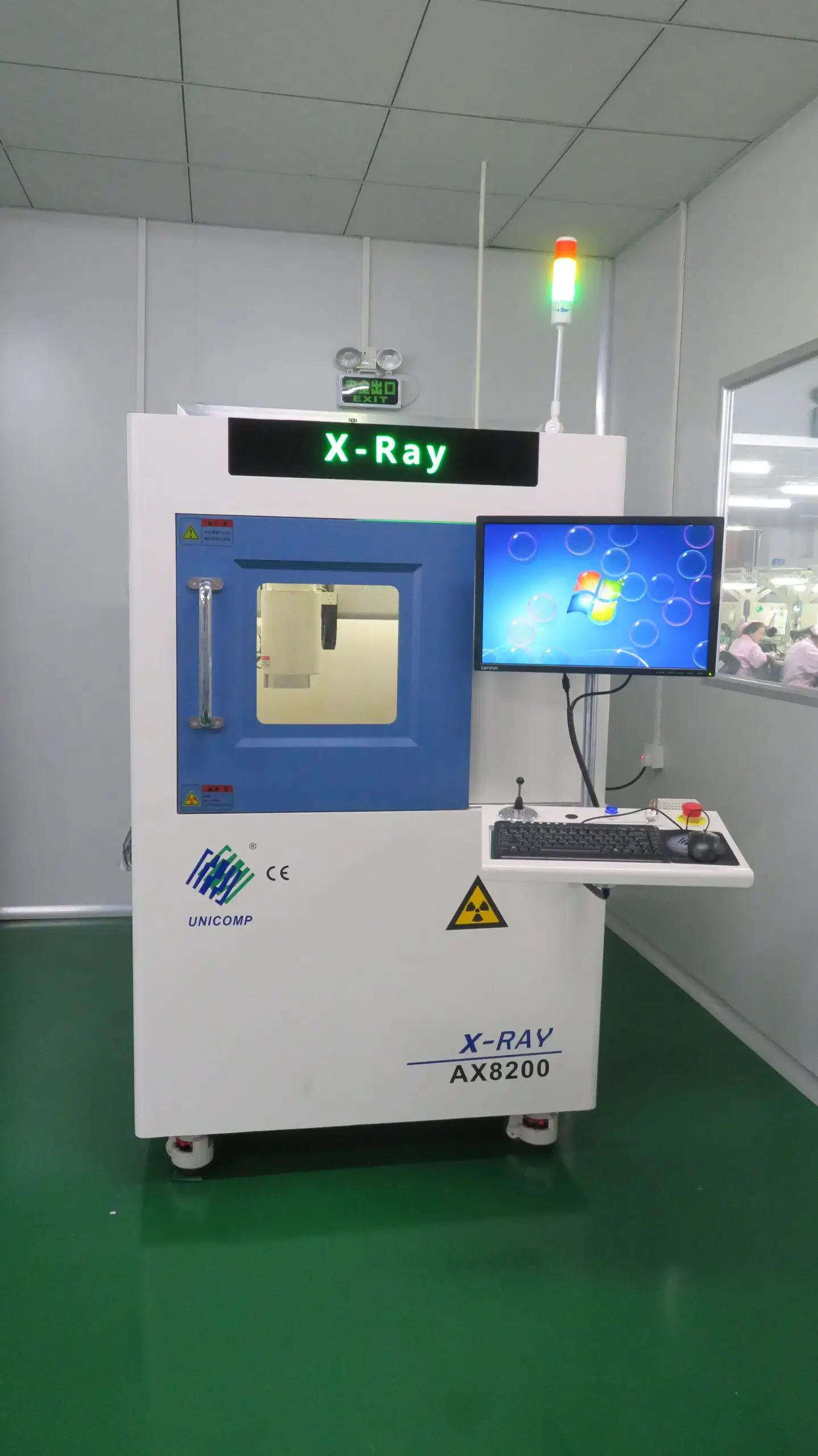
| X-Ray | Inspect hidden solder joints | BGA/QFN/LGA voids, internal bridging, insufficient solder, hidden opens | BGA, QFN, LGA, CSP, PoP |
| Flying Probe | Electrical verification without dedicated fixture | Connectivity, shorts, opens, basic component measurements | Prototype and low-volume |
| ICT | Fast node-level electrical test with fixture | Opens, shorts, component value, and orientation faults | Stable repeat production |
| FCT | Verify board operation | Power-up, I/O, communication, sensor, control, and firmware behavior | Functional products |
| Aging / Burn-In | Check early-life stability | Intermittent faults, thermal drift, early component failures | Reliability-sensitive products |
| Environmental Test | Verify performance under environmental stress | Temperature/humidity, thermal shock, vibration, drop, salt spray | Industrial, automotive, aerospace, outdoor |
| High-Voltage Test | Verify insulation and dielectric behavior | Leakage, breakdown, clearance/creepage failure | Power electronics |
| Solderability Test | Verify wetting capability of PCB finishes and component leads | Oxidation, poor storage, surface contamination, weak wetting | Incoming materials and failure investigation |
| Microsection Analysis | Inspect plated-hole and internal copper structure | Hole-wall plating, barrel condition, internal structure, joint cross-section | Failure analysis and high-reliability builds |
Common assembly defects and controls
- Solder Bridging — Causes: Excess paste, aperture or profile errors. Controls: Stencil and paste-volume control, thermal profile. Detection methods: 3D SPI, AOI, X-ray.
- Component Misalignment — Causes: Placement offset, paste imbalance, improper program. Controls: Fiducials, placement program, first-piece check. Detection methods: AOI, X-ray.
- De-Wetting — Causes: Oxidation, contamination, expired paste, poor storage. Controls: Correct cleaning, material storage, nitrogen reflow. Detection methods: Visual inspection, AOI, solderability testing.
- Tombstoning — Causes: Uneven wetting, thermal imbalance, aperture mismatch. Controls: Balanced stencil apertures, uniform heating. Detection method: AOI.
- BGA Void / Hidden Open — Causes: Paste issues, profile issues, warpage, or package issues. Controls: Paste design, baking, profile control. Detection methods: X-ray, functional test.
- Wrong Polarity — Causes: Mismatch between the BOM and drawings or a feeder setup error. Controls: Placement-data check, first-article inspection. Detection methods: AOI, FCT.
- Insufficient THT Fill — Causes: Thermal mass, hole and lead mismatch, wave setup. Controls: Preheating, flux, wave or selective profiles. Detection methods: Visual inspection, X-ray, microsection.
Which Standards Apply by Industry?
Assembly and quality standards currently being used include IPC-A-610J Class 2 and Class 3; IPC J-STD-001J; IPC J-STD-001JA and IPC-A-610JA for automotive assembly; and IPC J-STD-001JS for space and military assembly. Management and material standards include ISO 9001:2015/Amd 1:2024; ISO 13485:2016; IATF 16949:2016; RoHS 2011/65/EU as amended by (EU) 2015/863; and REACH Candidate List screening for SVHCs.
What Comes After Standard PCB Assembly?
How Are PCBAs Cleaned and Protected?
Flux cleaning removes all flux residues from the surface of a PCB before protection. Cleanliness verification provides assurance that the surface meets the required surface conditions. Protecting the assembly from moisture, dirt, chemical exposure, temperature extremes, and vibration is accomplished with acrylic conformal coating, selective coating, masking, and potting. Areas requiring electrical contact, adjustment, heat transfer, grounding, or later access remain masked. Coating thickness, coverage, cure condition, and uncoated keep-out areas are verified against the product requirements.
Rework And Repair
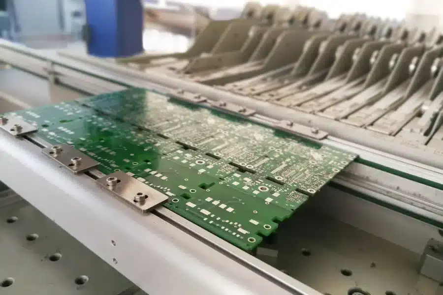
Rework includes hand soldering, BGA rework, part replacement, solder-joint repair, implementation of engineering changes, prototype fixes, and PCB revision corrections. The specific method used is determined by the components, joint types, pad condition, board construction, and allowable thermal exposure. Replacement parts and the applied change remain traceable to the repaired board or lot.
After completing rework, AOI checks visible component placement and solder quality. X-ray is used for BGA and other hidden-joint repairs. The function of the reworked board is confirmed through functional testing. The rework instruction is also synchronized with the BOM, placement data, and future production information when the change will continue into subsequent orders.
PCB Assembly Lead Time And Cost
| Project Type | Typical Production Window | Production Conditions |
|---|---|---|
| Assembly-Only Quick Turn | 2–5 days | PCBs and components available; standard SMT/THT; defined inspection |
| Prototype PCB Assembly | 3–7 days | Production files; available PCBs and parts; prototype quantity; standard test scope |
| Full Turnkey Prototype | 10–16 days | PCB fabrication, component sourcing, assembly, and inspection |
| NPI / First Article Build | 2–3 weeks | Engineering check, FAI, test-plan setup, and fixture/software preparation |
| Low-Volume Production | 2–4 weeks | BOM sourcing, batch scheduling, inspection, and functional test |
| Repeat Production | Planned from BOM and process history | Stable files, approved alternatives, existing stencil, program, and fixture |
Quick-turn lead-time factors
- BOM Line Count — A larger number of unique parts requires more sourcing, part verification, and feeder-preparation work.
- SMT Placements Per Board — Increasing the number of placements increases programming, setup, placement, and inspection time.
- Through-Hole Component Count — Manual insertion, selective soldering, and solder-fill inspection increase the labor time required.
- PCB And Component Readiness — Production and assembly cannot begin until the PCBs and complete material kits are available.
- Fine-Pitch And Hidden-Joint Packages — Packages such as BGA, QFN, LGA, and PoP require additional assembly-profile development and X-ray inspection.
- Programming Work — Device preparation, firmware version programming, and checksum storage require programming setup and software or hardware checks.
- Test Work — Fixtures, software, and functional-test instructions require preparation.
- Quantity — Large-quantity orders have different material, line, and inspection requirements from small-quantity orders.
PCB assembly cost categories
- PCB Fabrication — Layers, materials, sizes, surface finishes, HDI, impedance, and panelization.
- Components — MPN, quantity, availability, authorized sources, and alternatives.
- Stencil And Setup — Stencil types, programming, feeder setup, line changeover, and first-article inspection.
- SMT Assembly — Total placements, assembly sides, small components, and fine-pitch packages.
- Through-Hole Assembly — Pin counts, manual insertion, wave soldering, selective soldering, and hand soldering.
- Inspection And Testing — 3D SPI, AOI, X-ray, flying probe, ICT, FCT, and reliability testing.
- Programming And Protection — Firmware, cleaning, coating, potting, masking, and cure verification.
- Rework And Engineering Change — BGA rework, component replacement, implementation of revisions, and reinspection.
- Product Integration — Cable, wire harness, mechanical assembly, box build, and final system test.
- Packaging And Delivery — Labels, ESD packaging, moisture-barrier packaging, custom packaging, and shipping.
How Can PCB Assembly Cost Be Reduced?
Having complete and consistent files reduces engineering clarification. Approved alternative components reduce the risk of component shortages and redesign, while PCB fabrication and component sourcing can occur in parallel. Improved handling and production efficiency for panels with 50+ pieces are obtained through panelization. Full reels and standard trays reduce manual material preparation. Test coverage should follow product risk so that each method has a defined purpose and unnecessary testing does not add cost without improving the required verification.
Stable stencils, placement programs, reflow profiles, and test fixtures provide easier setup for repeat work. Clear DNP, polarity, and orientation data drastically reduce the amount of first-article correction required. The use of reusable firmware, fixtures, and test software considerably decreases the amount of assembly preparation work that must be completed before sending a PCBA for testing.
What Industries Does SUGA Serve?

Medical Devices
Medical-device assemblies consist of patient monitoring systems, diagnostic devices, medical imaging systems, and portable medical devices. The assembly focus for these types of assemblies includes fine-pitch placement, BGA and QFN assembly, MSL handling, cleanliness, component and printed circuit board lot traceability, firmware version control, and controlled substitutions.
ISO 13485 traceability requires documentation to be more in-depth than a standard test report. Expect lot traceability records for components linked back to the finished PCBA, not just the finished-board serial number. For devices that have direct contact with skin or fluids, cleanliness verification and MSL handling must be confirmed before quoting because it is much less expensive to specify a cleanroom-adjacent process than to retrofit one mid-project.

Industrial Automation
Industrial automation products consist of PLCs, sensor control modules, motor drivers, industrial interface boards, and other electronics installed in control cabinets. The vast majority of these assemblies use both SMT and THT in combination with various connectors, terminals, relays, and power components. In many instances, conformal coating, wide-temperature operation, and EMI-aware assembly are required due to the environmental conditions and interfaces in which the products are used.
As these types of products are often used for 10 to 15 years, there should be plans in place to source components based on an approved-alternative list rather than relying on one specific MPN, because the original MPN may become obsolete during the product lifecycle. The decision to apply conformal coating should not be based on default practice but instead on the installation environment. Applying conformal coating protects against dust and moisture in control cabinets, but it can also add costs and create challenges when performing field repairs, so the decision must be made on a case-by-case basis.
Automotive Electronics
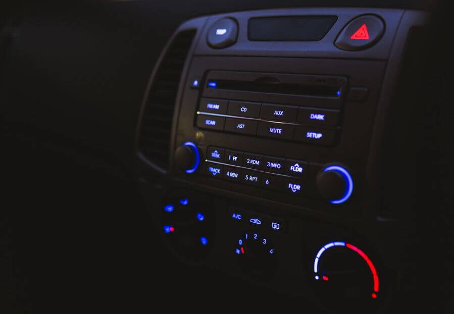
Automotive electronics consist of many different types of electronics, including ECUs, ADAS modules, lighting control modules, BMS controls, and in-vehicle control modules. The assembly focus for these products includes mixed-voltage systems, high-current connectors, thermal management, vibration resistance, component and process traceability, and a stable repeat-production environment.
For automotive customers, it is important to have dual-source qualification for the most critical components before production can commence, as a single-source component could be allocated and cause an entire vehicle line to stop. If a mid-lot BOM substitution occurs, even a substituted component deemed electrically equivalent must undergo partial first-article reverification under the IATF-controlled production process; therefore, it cannot be waved through with the remaining lot.

Aerospace And Defense Electronics
Assemblies in the aerospace and defense electronics category consist of navigation electronics, control systems, environmental systems, and communication and monitoring modules. For aerospace and defense assemblies, vibration loads are often a design consideration. Therefore, even if an SMT connector would work for an assembly, a through-hole connector with mechanical retention must be used when the load could create a vibration-induced fatigue failure rather than a soldering defect. These assemblies may require high-vibration control, thermal cycling, controlled-impedance boards, high-reliability soldering, and extended traceability.
Document retention for aerospace and defense electronics programs typically extends 7 to 10 years or longer. This must be considered when creating the process for generating and archiving test records and component lot data for these products.

Consumer Electronics
Consumer electronics are consumer products such as wearables, smart appliances, handheld devices such as mobile phones, audio products, remote controls, and game consoles. Typical assembly considerations are fine-pitch passive components; BGA and QFN packages; double-sided SMT assembly; compact panel design; rapid prototype iteration; and repeat-production cost control.
This industry tends to place greater importance on cosmetic inspection than other industries because a cosmetic defect can result in a return even when the board passes electrical testing, thus adding cosmetic criteria to inspection plans alongside functional criteria. Decisions regarding panelization and tooling made during the NPI phase are more important than additional test coverage once production volume ramps, as a prototype panel layout rarely scales cleanly to a 10,000-unit line change-over.

IoT And Wireless Devices
IoT and wireless devices consist of cellular sensor nodes, Wi-Fi and Bluetooth devices, smart meters, asset trackers, and wireless gateways. The focus of assembly for these products is RF-sensitive device placement, antenna-area control, compact BGA and QFN assembly, low-power design support, control over firmware and serial numbers, and interfaces for sensors and communications.
An antenna keep-out zone violation is one of the more common first-article failures because a component placed a millimeter into the keep-out zone may detune the antenna without producing any visible defect during AOI. Two or three placement-and-retest cycles may be required before communication tests pass consistently on RF prototypes.
Telecom And Datacom Equipment
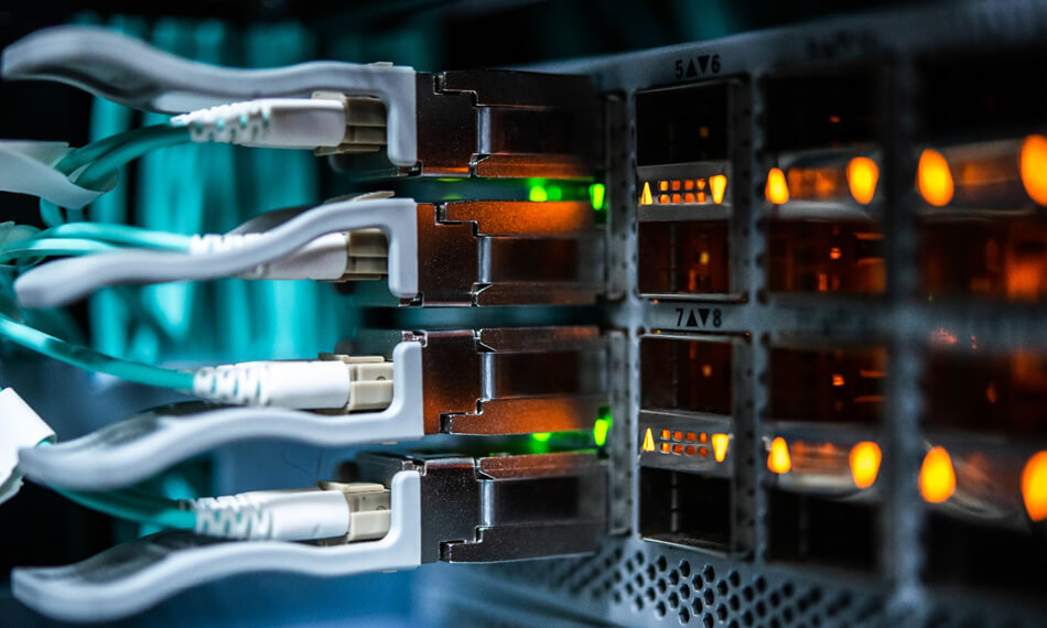
Telecom and datacom equipment consists of network control boards, communication interface modules, router and gateway modules, optical communication controls, and data-acquisition units. Controlled impedance, BGA, LGA, and QFN package types, high-speed connector placement, multilayer and HDI boards, programming, and interface traceability shape the assembly requirements.
Impedance-control tolerance is defined by the stack-up as well as the via structure, not just by the component choice. Therefore, a signal-integrity failure on a high-speed link can often be traced back to the via transition or reference-plane gap rather than to a defective part. Given that the sensitivity of multilayer and HDI boards is compounded, performing a DFM review of the stack-up before fabrication can identify problems that AOI and functional testing can only detect after the board is manufactured.

Power Electronics And Energy Systems
Products include power distribution units, inverter controls, charger controls, energy-storage BMS, and industrial power supplies. The work includes handling large through-hole components and high-current connectors, selective soldering, creepage and clearance control, thermal management, heavy-copper boards, and mixed SMT and THT assembly. Creepage and clearance distances follow the board's voltage class rather than a single fixed rule, so a layout suitable for 48 V must be re-verified when the design moves to a 400 V tier. Heavy-copper boards are also more prone to warpage during reflow, making early DFM review of the panel layout important before PCB fabrication.

Robotics And Motion Control
Robotics and motion-control products include robot controllers, motor-control boards, encoder interfaces, servo controls, and machine-vision support boards. Mixed assembly, connector orientation, vibration resistance, motor-current sections, firmware programming, and sensor and encoder interfaces constitute the main assembly considerations.
A connector installed in the wrong orientation is a minor rework at the board stage but a costly correction after the assembly has been integrated into a chassis with motors and cabling. When testing real-time control circuit boards, the functional test must exercise closed-loop operation, not just power-on and input/output continuity. Many boards pass static testing but fail when running a motor under load conditions.

Test And Measurement Equipment
These products include evaluation kits, monitoring systems, data loggers, signal-generation boards, and laboratory interfaces. They require frequent revision support, the use of precision analog components, low-noise assembly methods, programming, a calibration interface, and documented change control.
Test and measurement equipment runs are low-volume and high-mix; therefore, calibration-interface traceability should be tied to the individual serial number rather than throughput because one miscalibrated unit shipped to a laboratory can invalidate its test results. A high frequency of revision changes means tighter change control of DNP lists and BOMs than on a mass-produced board. Any missed revision flag on this type of equipment will directly change what it measures.
PCB Assembly Case
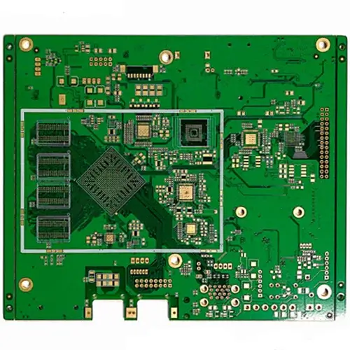
High-Density 8-Layer Control Board
Board Details
This project included the development and assembly of a prototype high-density control board for NPI. There are 8 layers on the board, with a thickness of 1.8 mm, 3 / 3.5 mil line / space, a minimum hole size of 0.2 mm, and a minimum hole-to-line distance of 0.13 mm. The outer copper was 1 oz, and the surface finish was ENIG.
Assembly Challenge
The assembly combined high-density multilayer routing in a limited space with fine-pitch packages, hidden solder joints, and tight hole-to-line geometry.
Process Used
The steps involved in this process were BOM and footprint checks, panel and fiducial checks, fine-pitch stencil control, BGA and QFN placement, a controlled reflow profile, and FAI.
Inspection And Functional Test
Printed solder paste was checked using 3D SPI. AOI was used to check the visible assembly conditions, and X-ray was used to check the hidden-joint packages. Electrical testing and workmanship verification completed the inspection.
Production Result
The mechanical and electrical requirements were verified.
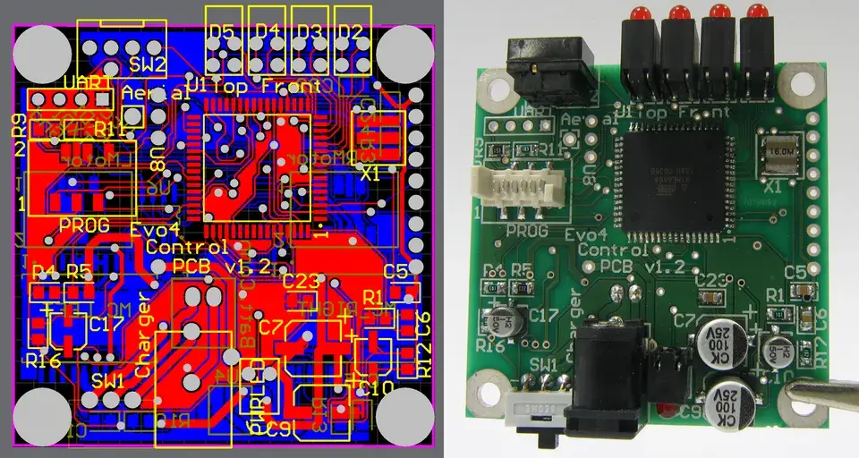
20-Unit Mixed SMT And Through-Hole Industrial Controller
Board Details
This project consisted of 20 fully assembled industrial-controller units, including PCB fabrication, full component sourcing, mixed SMT and through-hole assembly, connectors, larger through-hole parts, and functional I/O verification.
Assembly Challenge
Fine-pitch SMT and large THT parts were present in the same assembly. Connector orientation, different thermal loads, and repeatable low-volume setup required additional production controls.
Process Used
The steps used in this process were BOM verification, stencil-aperture optimization, SMT printing, placement and reflow, followed by selective soldering or hand soldering for through-hole components. Connector and polarity checks were included with FAI before completion.
Inspection And Functional Test
FAI and AOI were used with visual solder-fill inspection. Functional I/O testing verified that the required interfaces were functioning, while label and packaging verification checked the completed delivery condition.
Production Result
All 20 units were assembled and tested.
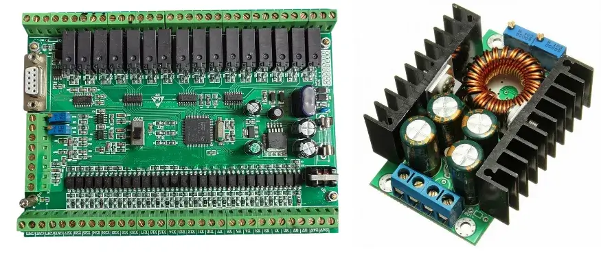
4 kV AC/DC Power Control Board
Board Details
The 4 kV AC/DC power-control PCB is a sizable board. Measuring 13 × 17.5 cm, the power-control PCB includes a control section that uses SMD parts together with THT parts and a high-voltage transformer. The construction of the board was completed in two stages. First, SMT-specific parts were sourced through partial-turnkey sourcing. Next, the larger THT parts and high-voltage transformer were prepared for the second assembly stage.
Assembly Challenge
In addition to having an SMT control section, this PCB has a high-voltage THT section. The assembly of both sections required attention to clearance and polarity control, large thermal mass, customer-provided high-voltage components, and correction of a BOM inconsistency before final assembly could occur.
Process Used
The PCB was fabricated and the SMD components were sourced simultaneously. As a result, the small SMD components were assembled first. Following this step, the large THT components were installed using a controlled preheat and soldering process. This portion of the assembly process also included clearance and connector-orientation verification. The previously identified BOM inconsistency was corrected with a one-day schedule adjustment.
Inspection And Functional Test
The staged assembly was verified through AOI, along with polarity checks, continuity inspection, PCB clearance checks, and solder-fill inspection. A staged high-voltage functional test verified that the assembled product met the required operating condition.
Production Result
All portions of the assembly, including the SMD control section, THT power section, and high-voltage function, were verified through testing.
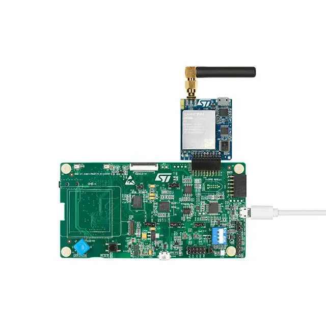
Cellular IoT Evaluation Board
Board Details
This is a cellular IoT evaluation board with the following elements: an ESP32, a SIM7080G cellular module, SIM and antenna interfaces, USB and UART communication, and firmware-controlled operation. The assembly utilized the revised PCB data and the intended communication and programming state.
Assembly Challenge
The assembly presented several challenges, including module-orientation control, fine-pitch component placement, cellular-area and antenna-area control, firmware-version control, and communication-interface verification.
Process Used
The process began with placement-data and revision checks, followed by module-orientation control, stencil and reflow-profile control, and component firmware programming. The serial number and checksum were documented in conjunction with FAI.
Inspection And Functional Test
The assembly was inspected using AOI for visible assembly conditions, while X-ray inspection was used to inspect the module and hidden joints. The subsequent functional checks included power-on, UART, USB, and cellular communication testing, followed by confirmation of the firmware version.
Production Result
The assembly was successfully completed and verified as functional.
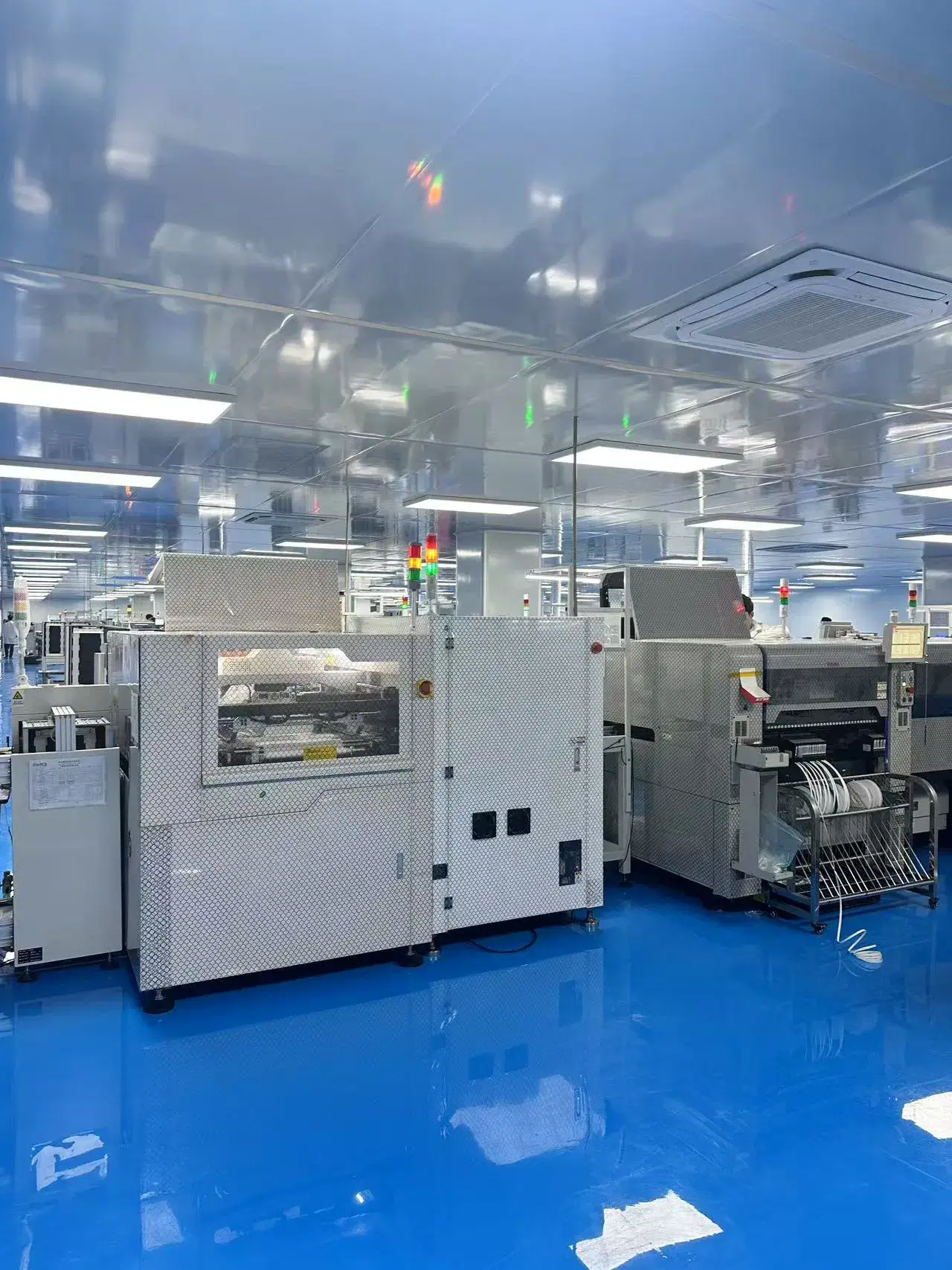
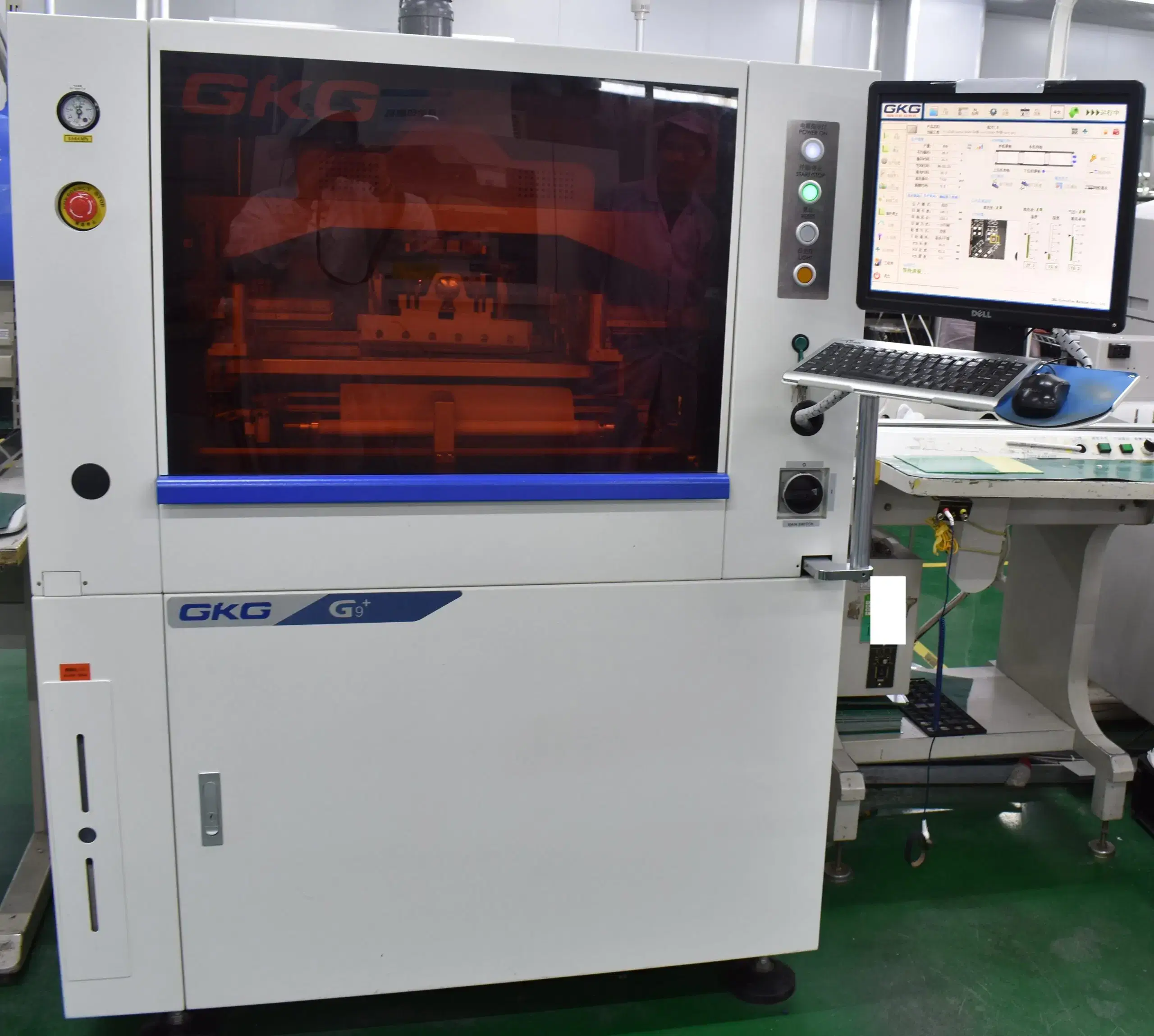
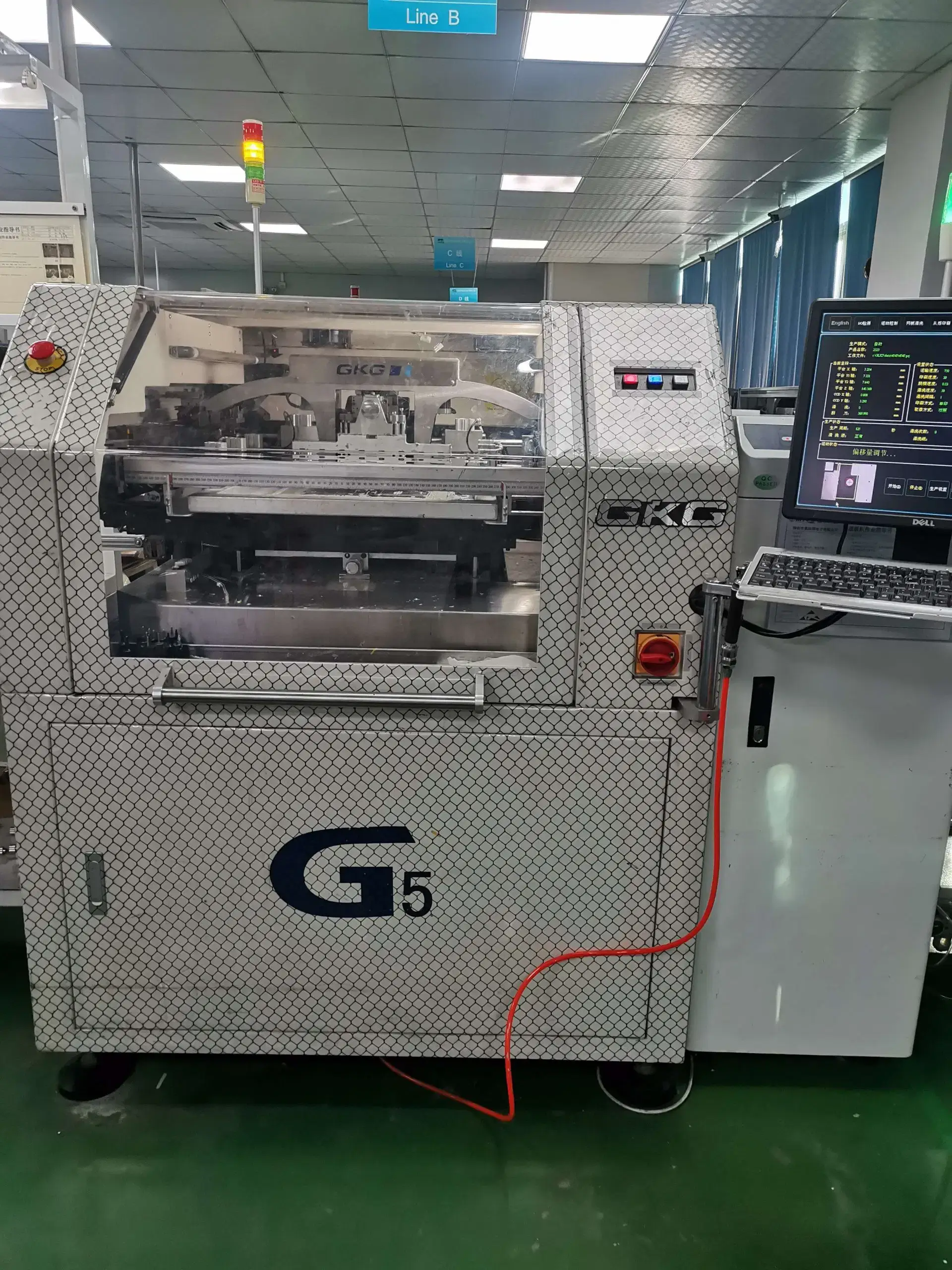
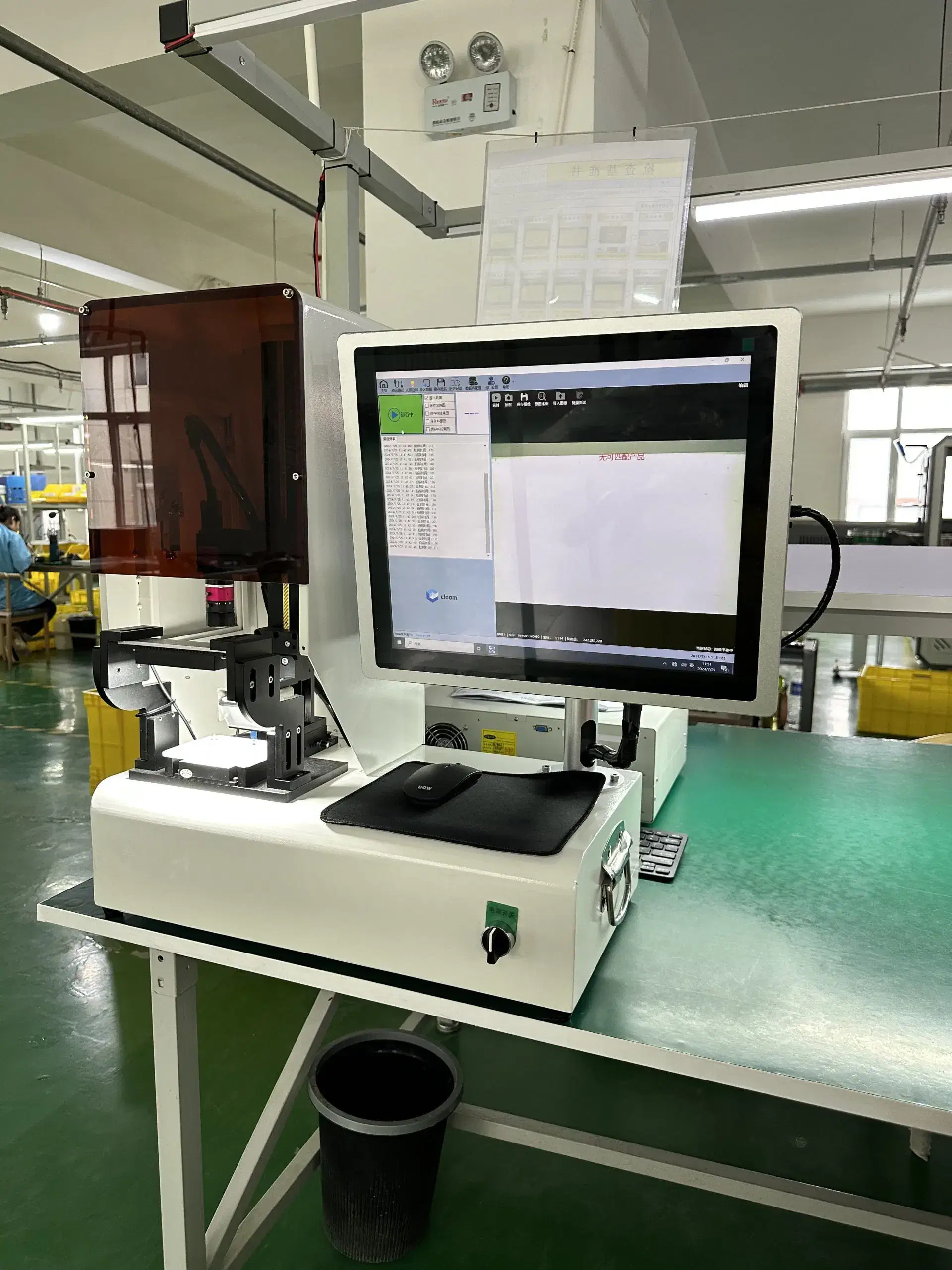
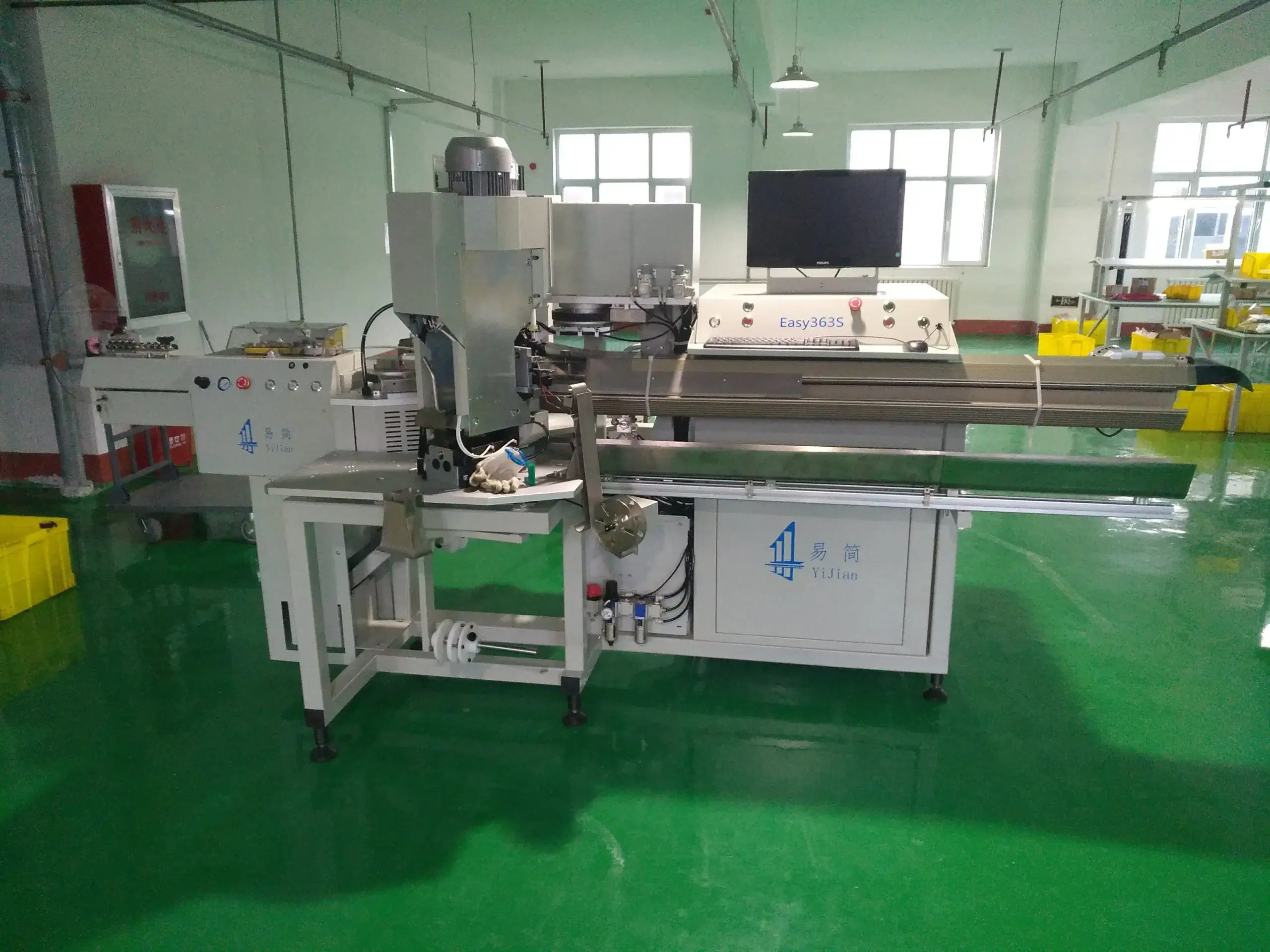
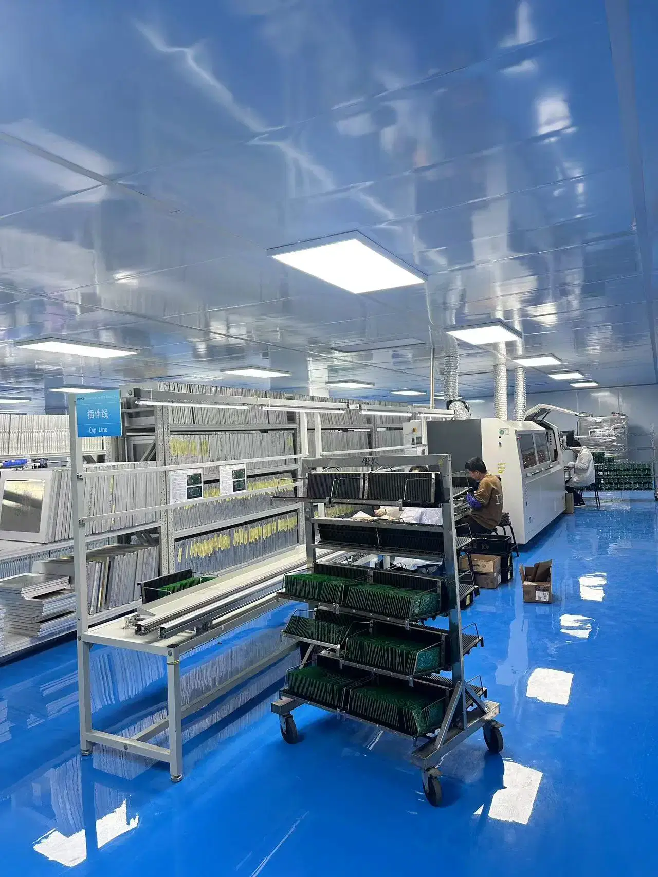
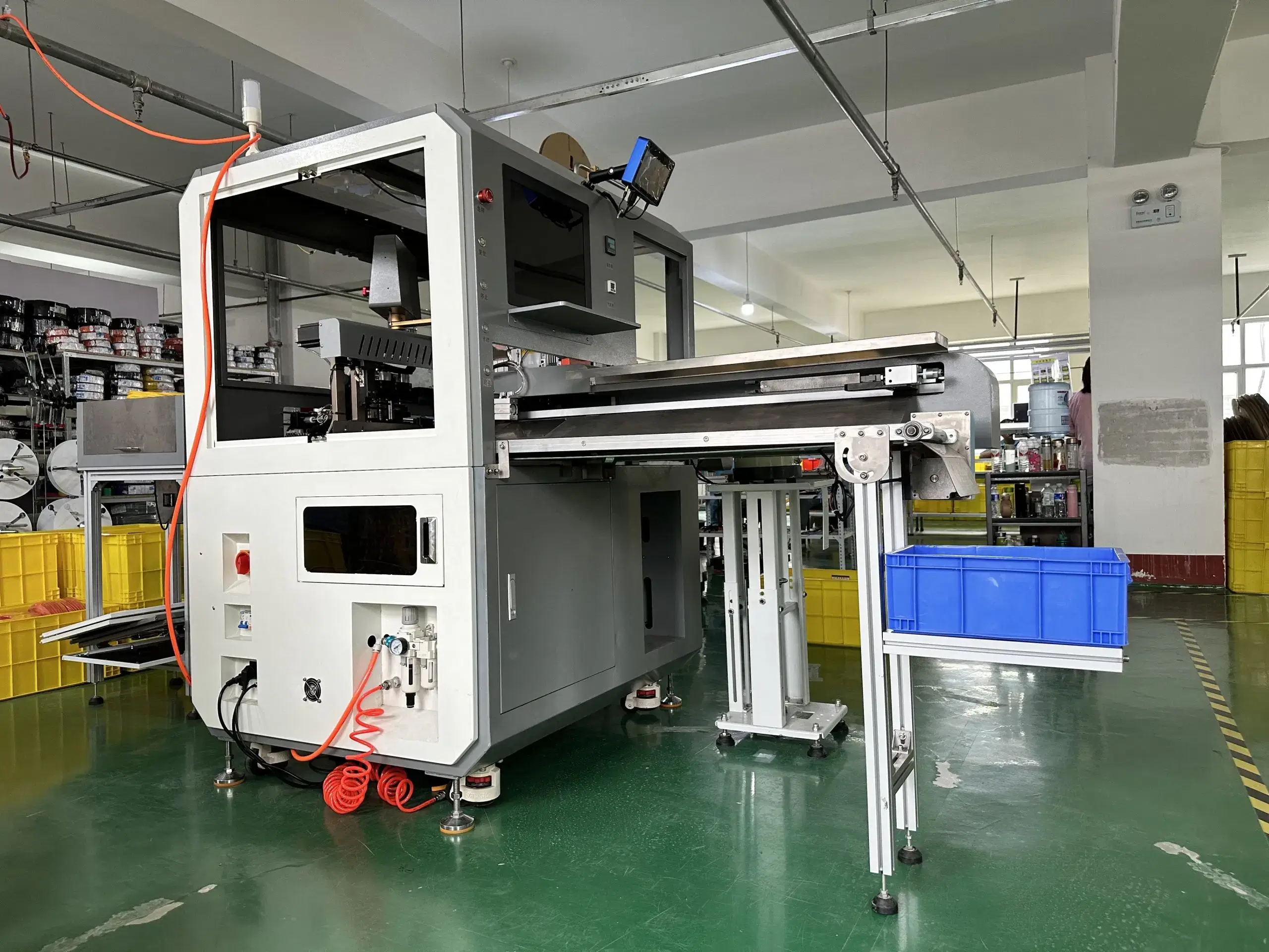
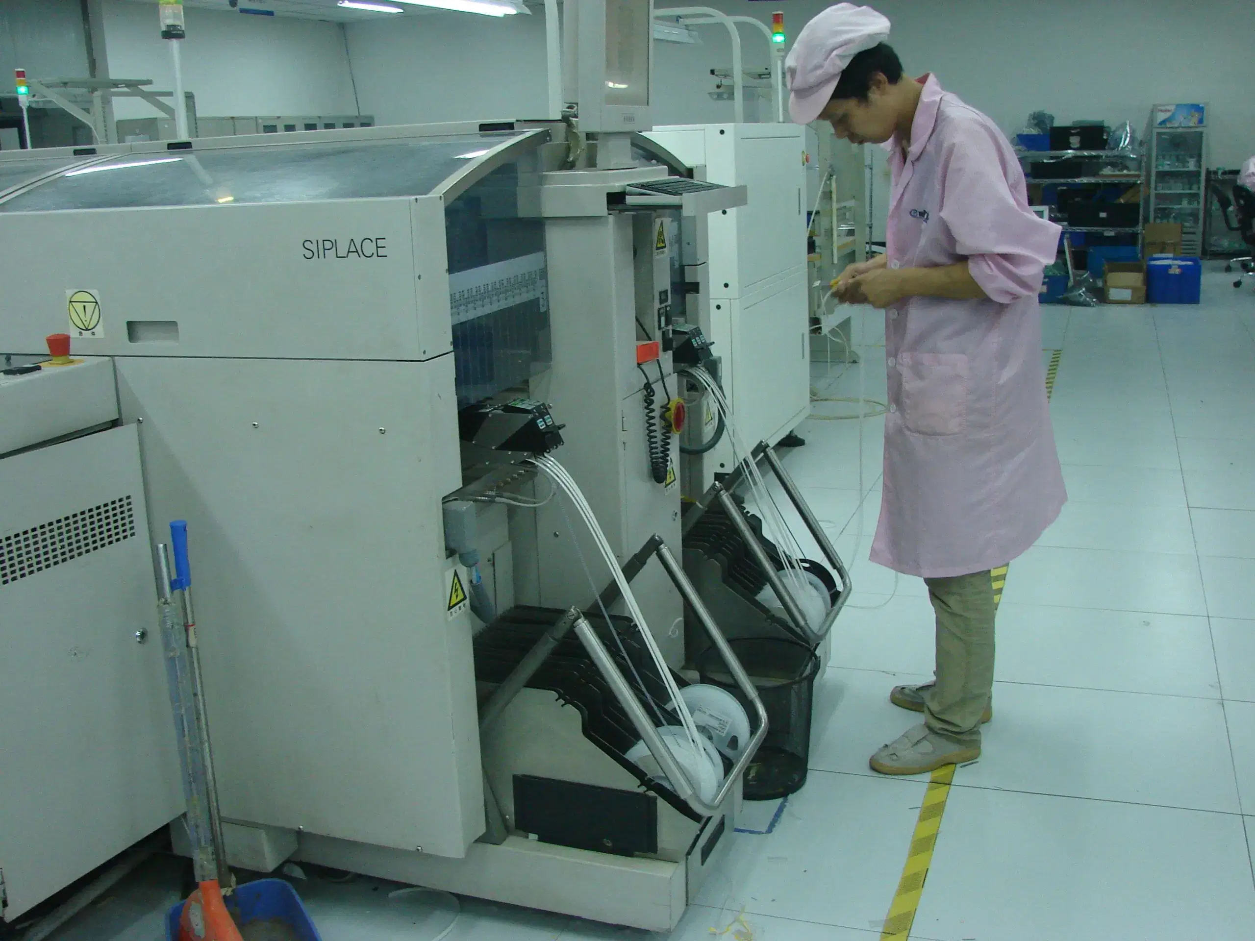
Our PCB Factory Gallery
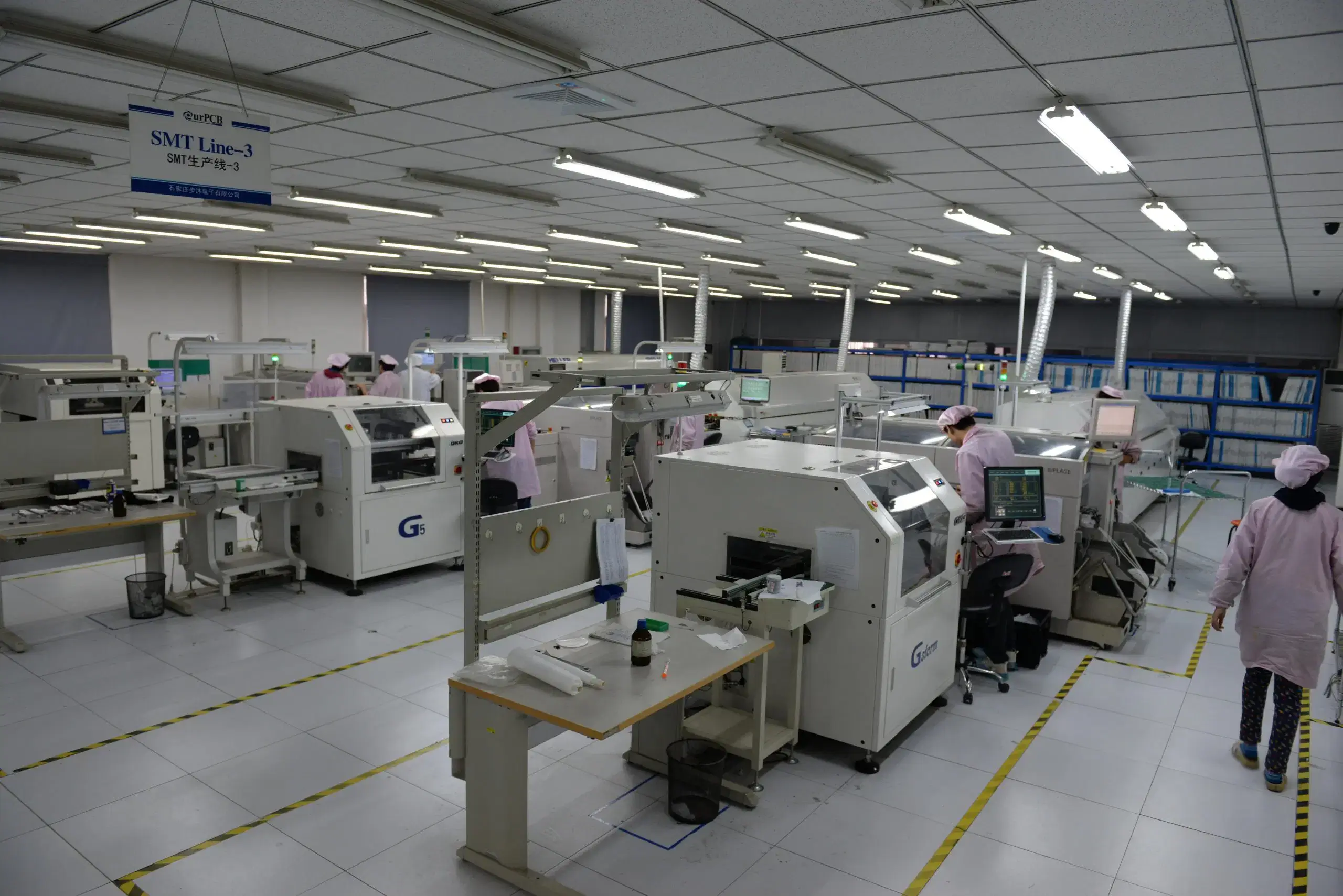
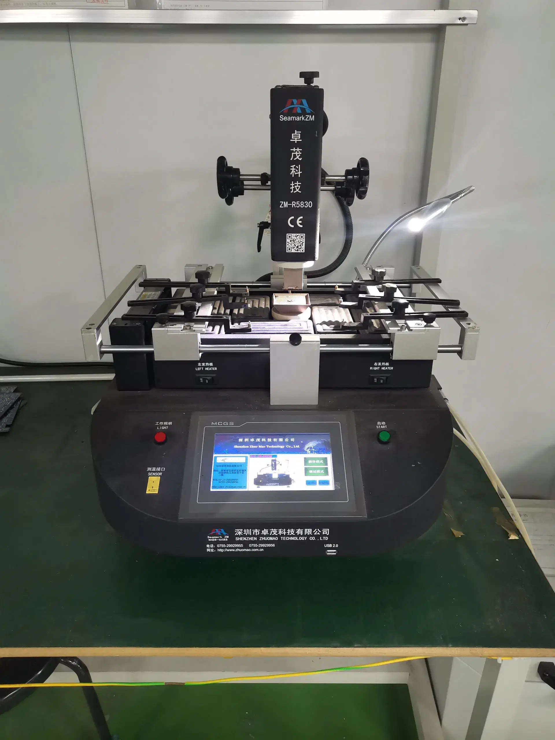
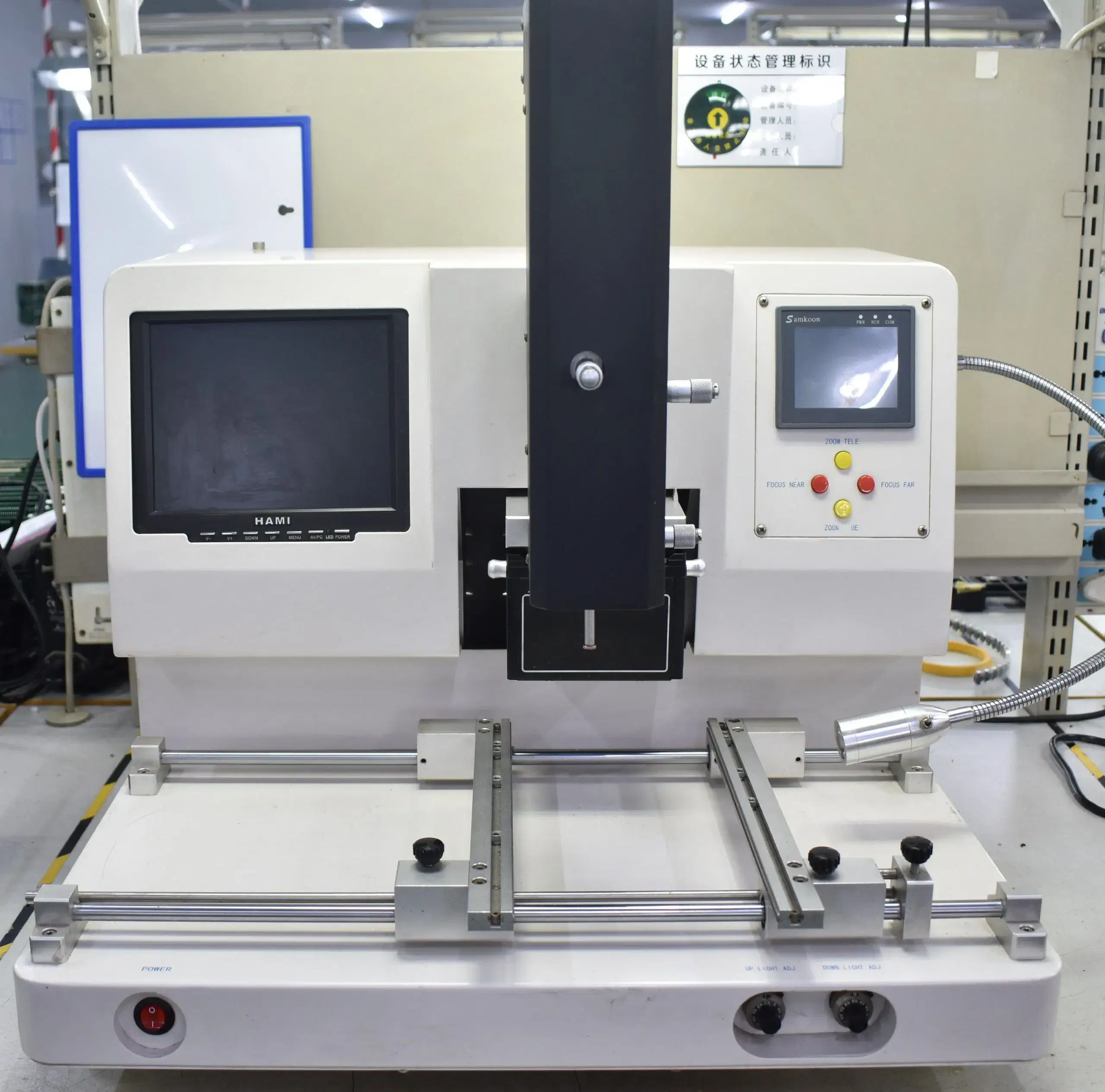
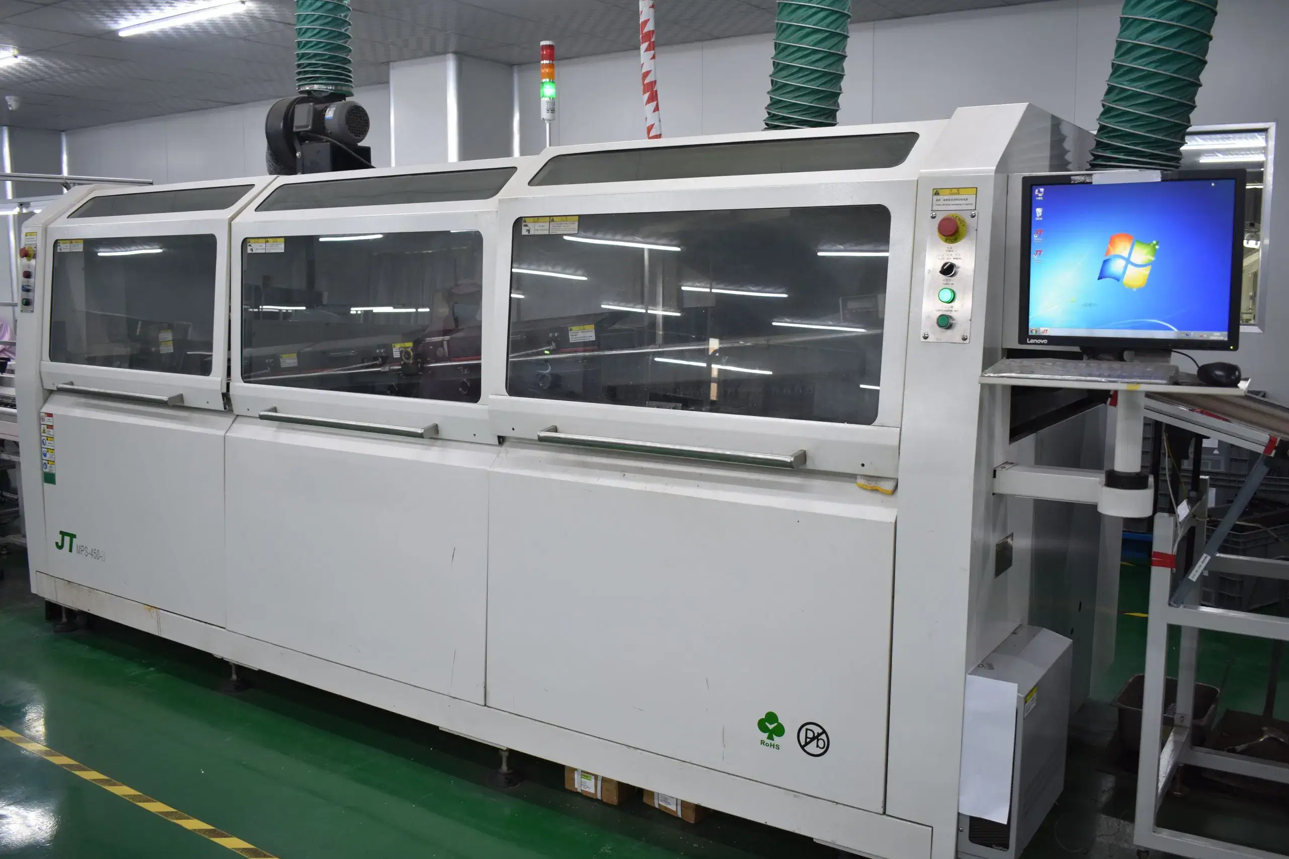
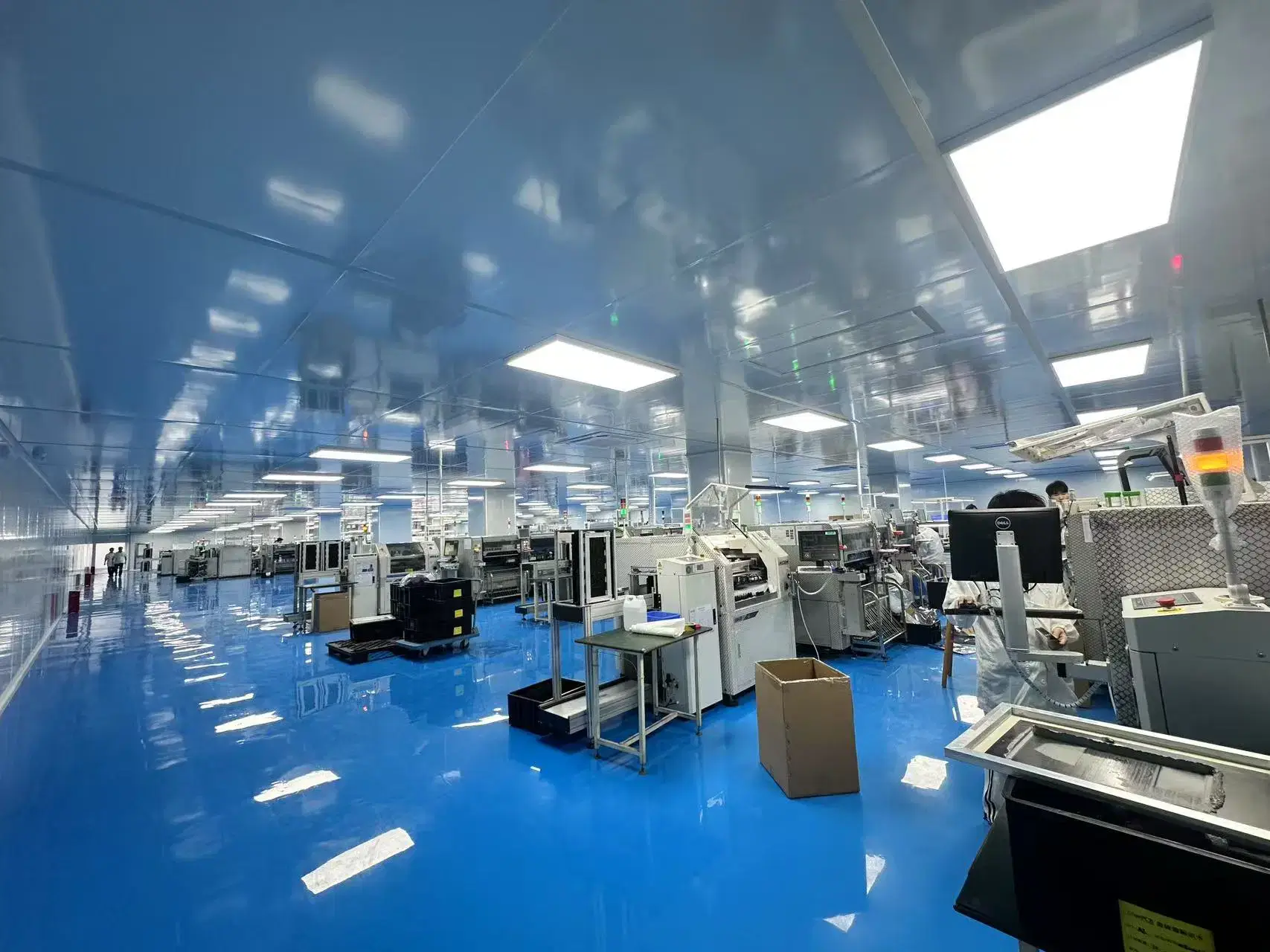
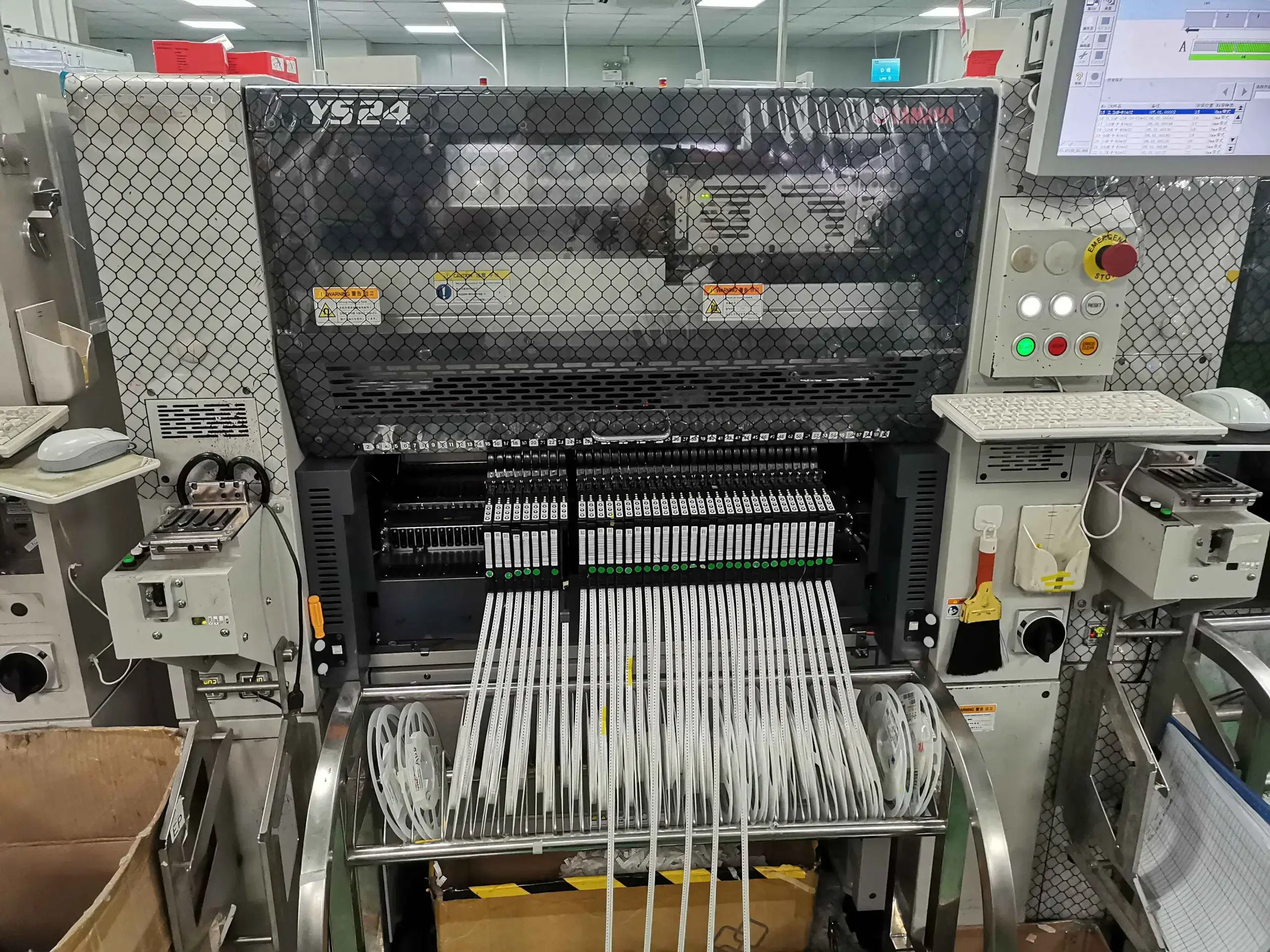
Frequently Asked Questions
The following component packaging formats are accepted: full reels, cut tape, trays, tubes, loose parts, and bulk through-hole components.
Customer-supplied components are checked against the BOM to ensure that the materials match the MPN, package, quantity, label, date code, moisture status, physical condition, and solderability.
Unused customer-owned parts, dedicated stencils, and test fixtures can be returned with the shipment or stored for future production runs.
Yes. Depending on the device, package, programming interface, and test strategy, ICs can be programmed before component placement or after PCB assembly. The firmware version, checksum, serial number, programming stage, and programming results are documented for traceability.
Yes. Both lead-free and leaded PCB assembly are supported by SUGA. This capability includes separate solder materials, reflow profiles, process controls, work instructions, and labels. RoHS-compliant projects use lead-free materials under the process specification, whereas leaded assemblies follow their own soldering profile and segregation procedures.
Yes. After PCB assembly, the work can continue into cable and wire-harness assembly, connector installation, mechanical assembly, enclosure integration, and final box build. This work may include displays, switches, fans, power supplies, labels, firmware loading, final system testing, and finished-product packaging within the same project.
For 0402, 0603, and 0805 passive components, prepare 20–30% extra or at least 20–30 additional pieces. ICs supplied on tape or reels generally require 2–3 additional pieces, while QFN, BGA, and other fine-pitch ICs may require 1–2 additional pieces, with more required for short tape. Connectors and other mechanical components typically require 1–2 additional pieces, while expensive or rare components require at least one spare.
Revisions made after First Article approval are treated as engineering changes. All Gerber files, BOMs, placement data, assembly drawings, firmware files, test instructions, and labels are reviewed for consistency with the new revision. Any affected stencils, placement programs, reflow profiles, work instructions, and test fixtures are updated, followed by a new or partial First Article verification before production resumes.