Upload BOM & Gerber
-
Mobile: +86 13312967631
-
Email: sales@sugaintl.com

Quick Turn PCB Assembly Services
China Fast PCB Assembly Supplier for Complex Prototypes and Time-Critical Production
SUGA coordinates engineering assessment, PCB fabrication, component sourcing, SMT/THT assembly, package-specific inspection, and board-level testing through one Shenzhen and Pearl River Delta supply chain.
1-40 Layers
Quick-Turn PCBA
0201 / 0.30 mm Pitch
Dense Assembly
What Is Quick Turn PCB Assembly?
Quick Turn PCB Assembly reduces the lead time for an assembled circuit board while keeping all steps in the manufacturing process intact, including engineering, sourcing, soldering, inspection, and testing.
| Service type | Primary goal | Main manufacturing work | Correct comparison |
|---|---|---|---|
| Quick Turn PCB Assembly | Compress the full manufacturing cycle for an assembled board | Engineering check, parts availability, stencil, placement, reflow, THT, inspection, and test | Inspected or tested PCBA versus inspected or tested PCBA |
| Quick Turn PCB Fabrication | Compress the bare-board fabrication cycle | Material, stack-up, imaging, lamination, drilling, plating, finish, and electrical test | Bare PCB versus bare PCB |
| Standard Production | Prioritize repeatability, capacity use, and unit cost | Stable materials, fixed processes, fixtures, testing, and volume scheduling | Repeat production versus repeat production |
Quick Turn PCB Assembly provides the quickest manufacturing option for an assembled circuit board while maintaining an engineering check and providing available components, a stencil, component placement, and reflow processes for soldering components onto a circuit board. Compared with standard production for inspected or tested PCBAs, Quick Turn PCB Assembly offers a much faster manufacturing cycle.
Quick Turn PCB Fabrication offers the quickest manufacturing cycle for bare circuit boards. The steps involved in bare circuit board fabrication include selecting materials, stacking materials, imaging, laminating, drilling holes in the circuit board, plating the circuit board, finishing the circuit board, and electrically testing the finished circuit board. Quick Turn PCB Fabrication provides bare circuit boards that have been inspected and electrically tested but not assembled.
Standard production is designed around repeat quantities and low unit costs. Materials used for standard production will be stable, established manufacturing processes and fixtures will be used, and volume scheduling will be applied. Standard production is designed to produce repeatable products based on the same materials and established processes.

Quick Turn vs. Standard Production
Quick Turn PCB Assembly reserves capacity earlier in the production process to coordinate engineering, manufacturing, and assembly activities associated with urgent decisions. In contrast, standard production focuses on producing repeat quantities of stable versions and lower unit costs for volume manufacturing. The Quick Turn path to manufacturing hardware can only be taken when board complexity, component availability, test coverage, and deliverable requirements allow it.
Why Bare-Board Speed Does Not Set the PCBA Date
The Gerber data and stack-up and drilling information control bare circuit board fabrication, while the BOM, centroid data, assembly drawing, stencil, and machine programs control assembly preparation. As a result, the two clocks are separate. A bare circuit board that is completed within 48 hours will not yield a finished PCBA within 48 hours if any components, stencils, machine programs, inspection limits, or test inputs are incomplete. The finished PCBA date follows the start of the assembly process and includes placement, soldering, inspection, testing, and delivery preparation.
When Quick Turn Accelerates Engineering Decisions
Quick Turn PCB Assembly creates earlier access to hardware that supports real engineering decisions. Examples include design iterations, NPI validation, urgent engineering samples, pilot runs, replacement control boards, and demonstration hardware. Stable versions with predictable demand can use standard production.
What Determines Quick-Turn PCBA Lead Time?
Quick Turn PCBA lead time is determined by the latest-ready requirement across engineering data, bare-board fabrication, component availability, assembly preparation, inspection, testing, and delivery. The sections below identify separate clocks for each of these processes to prevent confusion and clarify that a bare-board promise does not imply a complete-PCBA commitment.
When Does the PCBA Clock Start?
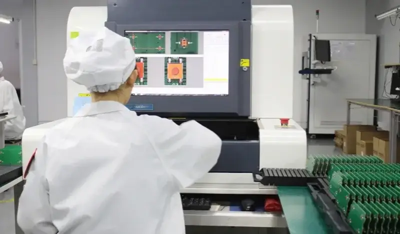
A manufacturing clock begins only when the following elements have been adequately defined for manufacturing preparation: file revisions, board requirements, BOM status, and test inputs. Manufacturing days, business days, calendar days, and shipping days describe distinct time frames within the manufacturing cycle. A design change, BOM change, or test-input change can move the manufacturing clock’s start point again.
| Manufacturing activity | Start condition | Engineering inputs / variables | Required output | Schedule control |
|---|---|---|---|---|
| Engineering preparation | File revision, PCB specification, and assembly requirements are available for engineering review | Gerber/ODB++; drill data; stack-up; BOM; centroid; assembly drawing; test inputs | Manufacturing-ready data package | Do not commit the finished-PCBA date until all file conflicts are resolved |
| PCB fabrication | Stack-up, material, copper, surface finish, and hole structure are confirmed | Layer count; board dimensions; HDI structure; via structure; material availability; surface finish | Electrically tested bare PCB | Track bare-PCB completion separately from finished-PCBA delivery |
| Component availability | BOM, MPNs, quantities, and substitution rules are confirmed | On-hand stock; authorized-distributor supply; constrained parts; obsolete parts; consigned components | Complete and authorized component set | Component shortages often determine the delivery date before assembly capacity does |
| Assembly | Bare PCBs, stencil, machine programs, and components are ready | SMT/THT process; single- or double-sided assembly; BGA; fine-pitch components; connector and mechanical load | Assembled PCBA | Double-sided assembly, mixed processes, and special components add setup and soldering operations |
| Inspection and test | Inspection methods and acceptance limits are defined | AOI; X-ray; flying probe; ICT; FCT; programming | Inspected and tested PCBA with available quality records | Keep all agreed inspection, programming, and test operations within the rush-production schedule |
| Delivery preparation | Agreed board-level inspection and test requirements are completed | Packaging method; labeling requirements; shipment method | PCBA packaged and prepared for shipment | State transportation time separately from manufacturing lead time |
What Extends PCB Fabrication Time?
PCB fabrication time depends on several factors, including PCB layer count, board area, material availability, and construction complexity. The higher the PCB layer count, the more inner-layer imaging, registration, lamination, drilling, and electrical-test work is required. HDI, via-in-pad, blind or buried vias, stacked microvias, heavy copper, and specialty materials increase the number of PCB fabrication and inspection steps and are scheduled separately. Simple, small-area boards may qualify for extra-urgent turnaround within 48 to 96 hours; refer to the planning benchmarks below for the specific ranges by PCB layer count.
What Delays Final PCBA Shipment?
Each shipment depends on having a complete kit; the percentage of BOM lines already purchased does not determine readiness until all required items are received. Shipment may be delayed by a missing processor, connector, oscillator, or programmed device because one missing part can hold the complete assembly. An alternative part must also receive authorization before machine programming and line preparation can continue.
Shipment may also be controlled by missing workmanship limits, unavailable tools or fixtures for programming and testing, missing programming files, golden boards, or pass/fail test instructions. The package mix determines which combination of AOI, X-ray, flying probe, ICT, or FCT is required to meet the customer specifications.
Refer to the benchmarks below to see the difference between the assembly-stage target and the complete-PCBA commitment.
| Order condition | Planning benchmark | Correct interpretation |
|---|---|---|
| Simple 2-layer assembly with bare boards and stocked standard parts ready | Assembly-only stage: as fast as 1 business day | This is an assembly-stage benchmark. It assumes a consistent data set, a complete kit, simple processing, and limited inspection depth |
| 14–40-layer bare PCB | 10–15 days | Area, material, hole structure, copper, finish, and lamination count determine where the order falls within the range |
| 41–64-layer bare PCB | Separate high-layer schedule (low-volume, specialized request) | Stack-up, material, area, via structure, and electrical-test planning are assessed as one high-layer project |
| Medium-complexity assembly | 3–5 business days after accepted bare boards, a complete component kit, and manufacturing-ready files | Standard BGA, double-sided work, or mixed technology may fit this range when inspection and test inputs are already defined |
| HDI or specialty-material PCBA | Separate complete-PCBA schedule | PCB fabrication and assembly are planned from separate readiness dates, then combined into one finished-PCBA commitment |
The following constraints can move either the fabrication date or the final shipment date, depending on where they enter the order.
| Constraint | Manufacturing effect | Schedule effect | Engineering response |
|---|---|---|---|
| Specialty or constrained component | Allocation, broker assessment or alternative evaluation may be needed | Can add days or weeks | Authorize a compatible alternative or accept the sourcing delay |
| Obsolete/end-of-life component | Original part may not be available | Can block production | Use verified stock, authorize a replacement or redesign |
| Incomplete Gerber/BOM/centroid consistency | Program and tooling preparation stops until the data agree | Start date moves until conflicts close | Resolve revision, polarity, footprint and reference-designator differences |
| Via-in-pad | Filled and plated-over via processing is added | Adds a fabrication cycle | Retain only where package escape or thermal/electrical design requires it |
| Blind/buried vias or stacked microvias | Laser drilling, filling, plating and extra lamination may be required | Moves order into HDI planning | Provide full drill maps and stack-up definition |
| Non-standard material | Material sourcing and specialized lamination may be required | Can extend fabrication schedule | Use stocked FR-4 where electrical and thermal behavior permits; retain specialty material where electrically necessary |
| Mixed surface finishes | Multiple plating routes and selective processing are required | Extends fabrication planning | Use one applicable finish unless the design needs mixed finishes |
| Hidden-joint inspection | X-ray setup and workmanship assessment are required | Adds a separate inspection stage | Keep X-ray where BGA/QFN/CSP evidence is required |
| ICT or FCT | Fixture/program/test input may be required | Setup may control the shipment date | Define coverage, limits and test responsibility before build start |
Time-Critical PCB Assembly Capabilities
SUGA offers quick-turn PCB assembly for rigid, flex, rigid-flex, and HDI PCBs using SMT, THT, mixed technology, fine-pitch leaded devices, BGA, QFN, and other bottom-terminated packages. Standard PCB scheduling covers PCBs with 1-40 layers. Layer counts above 40, up to 64, are infrequent requests outside standard capacity and require a dedicated schedule rather than reserved standard queue time. Customers with boards in this range should communicate the requirement early rather than assume that standard quick-turn production time applies.
Common constructions include 0.6–2.0 mm board thickness, 0.5–2 oz copper, 3/3 mil trace and space, 0.10 mm laser microvias, and 0.15 mm mechanical drilling. Localized 2/2 mil features, heavy copper, stacked microvias, 01005 placement, 0.25 mm pitch, specialty materials, and specialized finishes are planned according to the specific construction and package.

Which PCB Construction Fits Quick Turn?
Rigid multilayer PCBs support industrial controls, telecommunications, computing hardware, and test boards. The schedule depends on layer count, materials, and board area, while the stack-up and bare-board electrical test establish the fabrication condition.
Flex PCBs used in wearable devices, compact sensors, and dynamic interconnects must include the specified flex material, stiffener, panel support, and, when necessary, a handling plan. Material and fixture availability are the most critical scheduling controls for flex PCBs.
Rigid-flex PCBs used in wearable devices, medical development hardware, and folded products require bend-area control, assembly support, additional lamination work, and panel support while maintaining sufficient control during assembly.
HDI PCBs used for dense BGA fan-out, compact modules, and high-density computing require a microvia map, lamination sequence, and fill/cap definition. Laser drilling, filling, and repeated lamination can determine the fabrication completion date.
High-current and thermal boards used in power controls, motor drives, and energy systems require the copper weight, connector load, thermal design, soldering method, and load-test inputs to be defined before scheduling.
Which Assembly Technology Fits the Board?
The assembly technology that best fits different industry applications varies according to board type. SMT is normally used for applications that require high-density automated placement and therefore requires the proper process for each step, beginning with solder paste transfer, followed by SPI, automated placement, reflow soldering, AOI. THT applications primarily consist of products that contain connectors, transformers, and mechanically loaded components, which rely on either lead insertion and manual soldering or wave soldering. Some designs may also utilize more than one technology, such as a mixed SMT/THT assembly, in which the procedure is divided into multiple process steps that include soldering as well as separate setup and testing for both technologies. Sequencing, whether single- or double-sided, for each assembly type depends upon a combination of package style, board side, mechanical load, thermal sensitivity, and the soldering method being used.
How Are Fine-Pitch Packages Controlled?
Fine-pitch packages should have a separate process to document their control requirements. Package options for fine-pitch leaded and BGA assemblies for applications such as sensors, modules, processors, and communication boards require dedicated stencils, placement, board support during solder paste transfer, and assembly inspection methods. Package availability and inspection setup will typically affect the assembly schedule. The ability of the leads to remain coplanar with respect to each other, their general shape, the transfer of solder paste onto the pads, and the visibility of fillet formation all affect the quality of the finished leaded assembly. BGA assembly quality depends on pad design, solder collapse, reflow balance, and whether the assembly can be inspected using X-ray to determine whether the solder joints are properly formed. SUGA supports a pitch of 0.30 mm and uses a separate process plan for a pitch of 0.25 mm. The assembly documentation must clearly define the specifications and requirements necessary to produce a PCBA, including the package drawing, land pattern, stencil apertures, solder paste, placement program, reflow profile, and inspection method.
Complex Interconnect Fabrication
Digital communications, high-speed digital interfaces, and RF-related applications require PCBs to have controlled impedance. The PCB stack-up must be defined, meaning that the dielectric, copper, target, and tolerance must be established, and an impedance coupon or another form of verification must be provided. The schedule is directly related to the availability of the selected dielectric materials and the control of the fabrication process. Via-in-pad designs may require filling and capping and add drilling, plating, and planarization before assembly. The 0.10 mm value is for laser microvias, whereas the 0.15 mm mechanical-drilling capability must be considered in conjunction with the thickness and aspect ratio of the board. The fabrication drawings must state whether the hole value refers to the drill-tool diameter or the finished-hole diameter to ensure that the manufacturing target is known.
What Can Each Inspection Method Prove?
Visual inspection is used to identify visible defects, such as broken components, the presence or absence of components, their orientation, including whether they are correctly placed or rotated, and the level of workmanship, providing a baseline for visually checking THT and manual assembly areas. Visual inspection cannot determine whether every electrical net is connected correctly, inspect hidden joints, or guarantee complete electrical functionality.
AOI examines visible solder connections on the PCB, verifies the alignment of components with the design intent, and assesses visible solder quality on standard SMT and double-sided assemblies. The AOI machine cannot inspect the bottom-side solder geometry of BGA or QFN packages or detect hidden solder voids.
The X-ray process examines the geometry of hidden joints, determines the location and size of bridging, open-joint indications, and voids in BGAs, QFNs, CSPs, or other bottom-terminated packages, and documents internal solder relationships. However, X-ray inspection cannot be solely relied upon to validate complete electrical continuity, proper firmware function, signal integrity, or product functionality.
Flying probe checks opens, shorts, nets, and selected component measurements on prototypes and low-volume boards without a dedicated fixture. ICT is more applicable to repeat production where fixture economics support connectivity, component presence or value, and circuit-node checks. FCT executes customer-defined board-level operation when test instructions, fixtures, firmware, and limits are available. These methods answer different questions; none alone establishes system certification, lifetime behavior, or final product approval. Regulated or high-reliability projects also need inspection limits and records tied to the board revision and lot.
How the Quick-Turn Process Works
SUGA compresses the idle time between these activities and moves compatible preparation tasks in parallel.
| File or input | Common format | Manufacturing purpose | Consistency rule |
|---|---|---|---|
| Gerber / ODB++ | RS-274X, Gerber X2, ODB++ | Copper, mask, silk, paste and fabrication artwork | Layer names, polarity, revision and aperture data |
| Drill files | Excellon | Hole positions, sizes and drill structure | Plated/non-plated identity, tool map and layer pairing |
| Stack-up / fabrication drawing | PDF, spreadsheet or controlled drawing | Layer order, dielectric, copper, impedance and material | Total thickness, copper, material and impedance target |
| Bill of Materials | XLSX/CSV | MPN, quantity, reference designators and procurement | MPN, package, lifecycle, quantity and authorized alternatives |
| Pick-and-place / centroid | CSV/ASCII | X-Y placement coordinates, side and rotation | Reference designators, origin, rotation and board side |
| Assembly drawing | Polarity, component location and special assembly notes | Orientation, do-not-fit items and mechanical restrictions | |
| Netlist | IPC-D-356 or equivalent | Bare-board electrical connectivity or test preparation | Revision and net consistency |
| Programming/test input | Binary, scripts, test instructions, limits | Programming and customer-defined board-level verification | Version, fixture, connection, limits and pass/fail criteria |
Engineering Alignment Before Manufacturing
Before manufacturing, engineers must first evaluate potential issues with the product design using DFM, DFA, and DFT processes. Engineers collaborate with manufacturers to ensure that all product information is coordinated across the following areas: Gerber or ODB++ files, drill files, stack-up construction drawings, BOM, centroids, assembly drawings, programming, and testing documentation. Some typical examples of quick-turn blocking issues are a BOM package that does not match the PCB land pattern, a centroid rotation that conflicts with the assembly drawing, missing polarity markings, and “do-not-fit” components still listed in the machine data. Closing these types of conflicts before tooling is produced provides manufacturers with manufacturing-ready data and keeps the rush schedule from being consumed by unnecessary reprogramming and rework.
PCB Fabrication and Component Availability
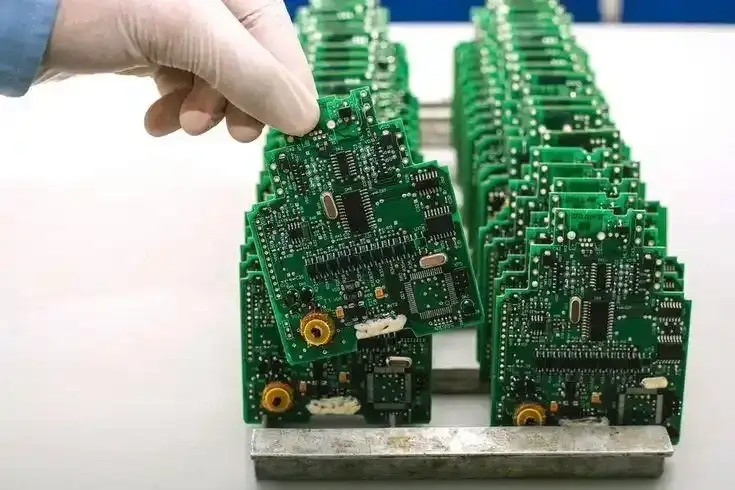
PCBs and components can be procured and manufactured in parallel. However, before line preparation can begin, both the board plan and component kit must be stable enough for programming. PCB fabrication produces acceptable bare boards after completing the specified stack-up, drilling, plating, imaging, finishing, and electrical testing operations, while component procurement provides the components through authorized purchasing, incoming verification, and component kit preparation. All sourcing models, whether managed sourcing, partial sourcing, or consigned, require incoming verification and quantity reconciliation; the only difference is who purchases the components. Alternate components are included in the build only if all of the following conditions have been met: the component’s package is acceptable, the component’s electrical function is acceptable, the component’s temperature rating is acceptable, and the component’s lifecycle status is acceptable.
How Are Special Assembly Operations Sequenced?
The sequence of assembling an SMT board follows paste printing, the use of SPI if package risk is present, component placement, and then the reflow process. If the board requires a second-side cycle, that cycle produces the completed SMT-populated board. THT insertion, which can be completed using wave or selective soldering, as well as press-fit, programming, and controlled manual operations, occurs based on connector load, the overall heat sensitivity of the assembly, and access. For boards with mixed technology, sequence matters; if a heavy connector or heat-sensitive component is used, it may have to be installed after reflow. Conversely, programming and press-fit operations may require access before the assembly is packaged for shipment.
What Proof Ships With the Assembly?
Inspection and testing produce the required evidence for shipment through a combination of visual inspection, AOI, X-ray inspection, flying probe testing, ICT, or FCT. The shipment record set may consist of AOI results, X-ray images or dispositions, electrical test results, the programming version used, functional pass/fail data, and the lot number or assembly identification. After completing all checks, the specified cleaning, packing, and labeling prepare the PCBA for shipment. The exact contents included in the record set depend on the package mix and any other testing work performed. Retaining the results, programming version, assembly identification number, and lot allows builds produced under the same manufacturing conditions to be compared.
Quick-Turn Cost Drivers
The dominant driver differs by project, so each order needs its own cost breakdown.
| Cost driver | Added resource or operation | Why cost increases | Practical response |
|---|---|---|---|
| Rush scheduling | Priority queue, parallel engineering and tighter coordination | Capacity and engineering attention are reserved earlier | Use the shortest service only for the stage that is truly schedule-critical |
| PCB layer count | Additional imaging, lamination, drilling, plating and inspection | More fabrication operations and process control | Reduce layers only when electrical and routing requirements allow |
| HDI / microvias / via-in-pad | Laser drilling, filling, capping and extra lamination | Additional HDI cycles and tighter registration | Retain only design-required structures; provide full drill and stack-up data |
| Fine pitch / 01005 / BGA / QFN | Stencil control, SPI, placement control, reflow and X-ray | Higher process-control and inspection demand | Use package density appropriate to the product; do not downgrade required packages only for price |
| Specialty materials | Dedicated procurement, lamination and handling | Lower stock availability and special processing | Use FR-4 when electrical and thermal behavior permits it; retain RF, thermal, or flex material when package risk calls for it |
| Component shortage | Expedited logistics, alternative assessment or verified secondary stock | Procurement risk and engineering assessment increase | Authorize alternates early and finalize the BOM |
| Prototype quantity | Tooling, stencil, programming and setup spread over few boards | NRE is distributed across fewer boards | Order enough units to cover engineering, rework and test needs |
| ICT/FCT/programming | Fixture, software, test engineering and execution | Test setup may exceed assembly setup | Match coverage to product risk and repeat volume |
| Revision changes | New files, stencil, program, sourcing or rework | Previously prepared work must be repeated or controlled | Lock each build revision and document authorized changes |
| Special handling | Moisture control, baking, conformal coating, selective soldering or special packing | Additional controlled operations are required | Specify only necessary special processes and workmanship requirements |
Removing X-ray, electrical testing, programming, or FCT lowers cost by removing the defect or function coverage provided by those test steps. Therefore, reducing test steps should be treated as a coverage decision rather than a price-only decision.

What Does Rush Scheduling Actually Add?
There is no fixed industry percentage that applies to every project. A longer lead time may help alleviate scheduling pressure, but other factors still affect the schedule, including obsolete components and unresolved design issues.
How Manufacturing Complexity Changes Cost
The manufacturing complexity factors that affect manufacturing costs include stencils, fixtures, programming, and engineering preparation, which are primarily setup costs. The selected material, layer count, plating, and assembly time determine the recurring costs of the PCB. Recognizing the distinction between one-time setup costs and recurring unit costs makes prototype and repeat-order pricing easier to compare.
How Parts Availability Changes Cost?
Parts availability can affect the final cost through premium freight costs, MOQs, verified secondary stock, and the engineering time required to find alternatives. A low-cost replacement may ultimately increase the total project cost if it requires modifying the land pattern, programming, thermal performance, or test limits. An appropriate measure for evaluating cost is the cost of an accepted, buildable kit rather than the quoted price for each BOM line.
What Makes a Quick-Turn Manufacturer Credible?
SUGA’s PCB/PCBA team has more than 30 years of manufacturing experience. IPC-A-610J and J-STD-001J address assembly acceptability and soldered-assembly requirements, while the specified class must match the requirements of each individual order rather than relying on general industry labels.
Credible quotations from quick-turn manufacturers will typically show:
- Whether the date covers bare boards, assembled boards, inspected boards, or tested boards.
- The layer count, board area, material specifications, via structure, surface finish, and assembly complexity used to determine the completion date.
- Whether the component kit is in stock, available from a supplier, constrained, consigned, or dependent on an alternative.
- Which hidden-joint, electrical, programming, or functional checks are included.
- Which inspection or test records will remain linked to the associated assembly and lot.
Can Manufacturing Data Stay Consistent?
When an assembly, kit, or components are produced, how can the manufacturing data remain consistent and accurate? Verification of consistent and accurate data is found in the agreement between all documents used to create the manufacturing data, including the BOM, fabrication data, assembly drawing, program version, and test instructions. If a change is made to one of the files, all corresponding files affected by that change must be identified, and the impact on the schedule must be recalculated.
Quick-Turn PCBA Applications
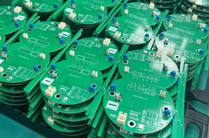
Quick-turn assembly is most effective for a small production run of hardware to resolve an unknown design, interface, or manufacturing issue before the product goes into wider production. Quick-turn applications will prioritize different types of risks, but the assembly, components, inspection, and test deliverables must all be specifically defined.

Medical Diagnostic Boards
Medical diagnostic and monitoring PCBs carry low-level analog signal paths. Flux residue from soldering a PCB could create leakage current across these analog paths at levels below what an industry-standard cleanliness check can detect. This leakage current can create a shift in sensor readings before the change is detected. Quick-turn assembly links cleanliness limits to the actual sensitivity of the signal being measured instead of an arbitrary standard of cleanliness because visual inspection is typically insufficient to detect this failure mode. Quick-turn PCB records provide a foundation for the development process, while clinical validation and final product approval remain separate processes.
Industrial Control Hardware
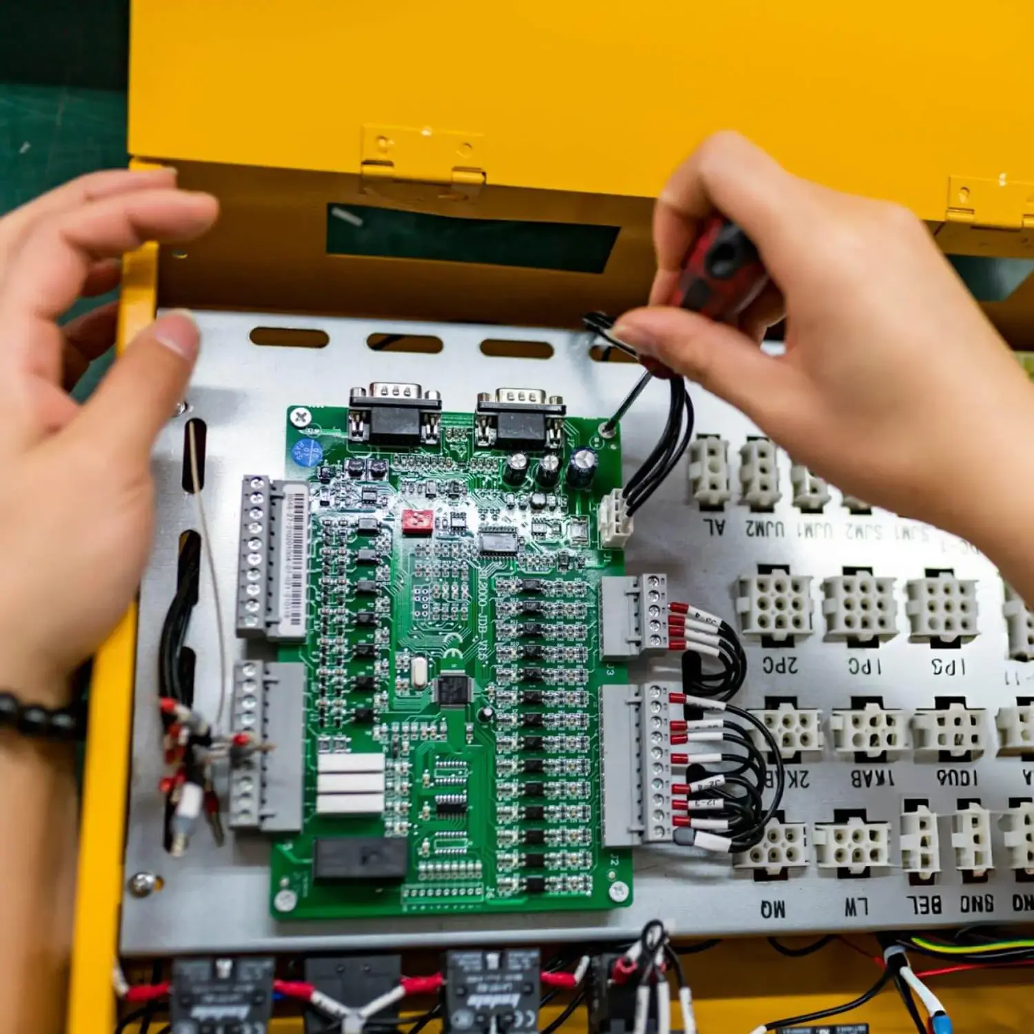
Industrial control PCBs are typically housed in control cabinets that are subjected to vibration, dust, and extreme temperature changes. Over time, these environmental conditions can deteriorate connector seating and reduce connector clearance. A static bench test cannot identify connector-seating and clearance issues. Quick-turn assembly checks connector orientation, mechanical clearance, and fixture access against the known profile of the control cabinet before vibration and thermal testing confirm long-term performance and before fixtures or larger production runs are released.
Some motor-control and power-control PCBs incorporate thermal cycling between the switching section and adjacent low-voltage logic circuits. This thermal cycling can compromise isolation clearance long before FCT discovers the failure condition. The quick-turn PCB provides an inspected baseline for design and process validation under a specific load condition.

Automotive Electronic Modules
Automotive electronic modules go through extreme thermal cycling from roughly -40C to 125C, whereas consumer electronic modules do not. Thermal cycling creates fatigue in BGA solder joints during use. Quick-turn assembly provides an initial solder-joint, connector-seating, and inspection baseline before thermal-cycling and vehicle-level reliability testing confirm the continued performance of the assembly. The record created establishes a baseline for design iterations. Vehicle qualification testing and component lifetime testing remain separate program activities.

Compact Consumer Devices
Compact consumer electronics are designed with fine-pitch components next to the battery connector. This means that when a product is dropped or flexed, there is an increased likelihood of bridging a joint and creating a short. A static continuity test cannot predict this bridging. Component clearance, connector alignment, and joint integrity at this junction are confirmed in the first batch of assemblies. Enclosure-fit and drop testing then confirm the performance of these components under normal handling.
Dense multilayer constructions must have stable registration and drill-to-copper clearance. A properly approved design, including the safety margin at the battery junction, must be replicated in subsequent batches.
Connected Sensor Hardware
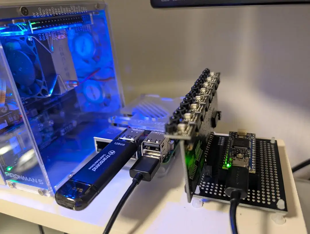
Connected sensors, IoT nodes, and wearable devices place components very close to the antenna keep-out zone. If just one component is placed incorrectly, it can detune the antenna; this cannot be identified using AOI or continuity testing. Placement is checked against the keep-out zone, along with power-rail behavior and connector access. Radio performance is validated after the enclosure has been built and tested for antenna and RF performance.
Rigid-flex configurations must have controlled support during printing and reflow because bending too close to the antenna trace can change the detuning risk. The completed boards provide traceable hardware for evaluating firmware, interfaces, and sensors.
Telecom Equipment Modules
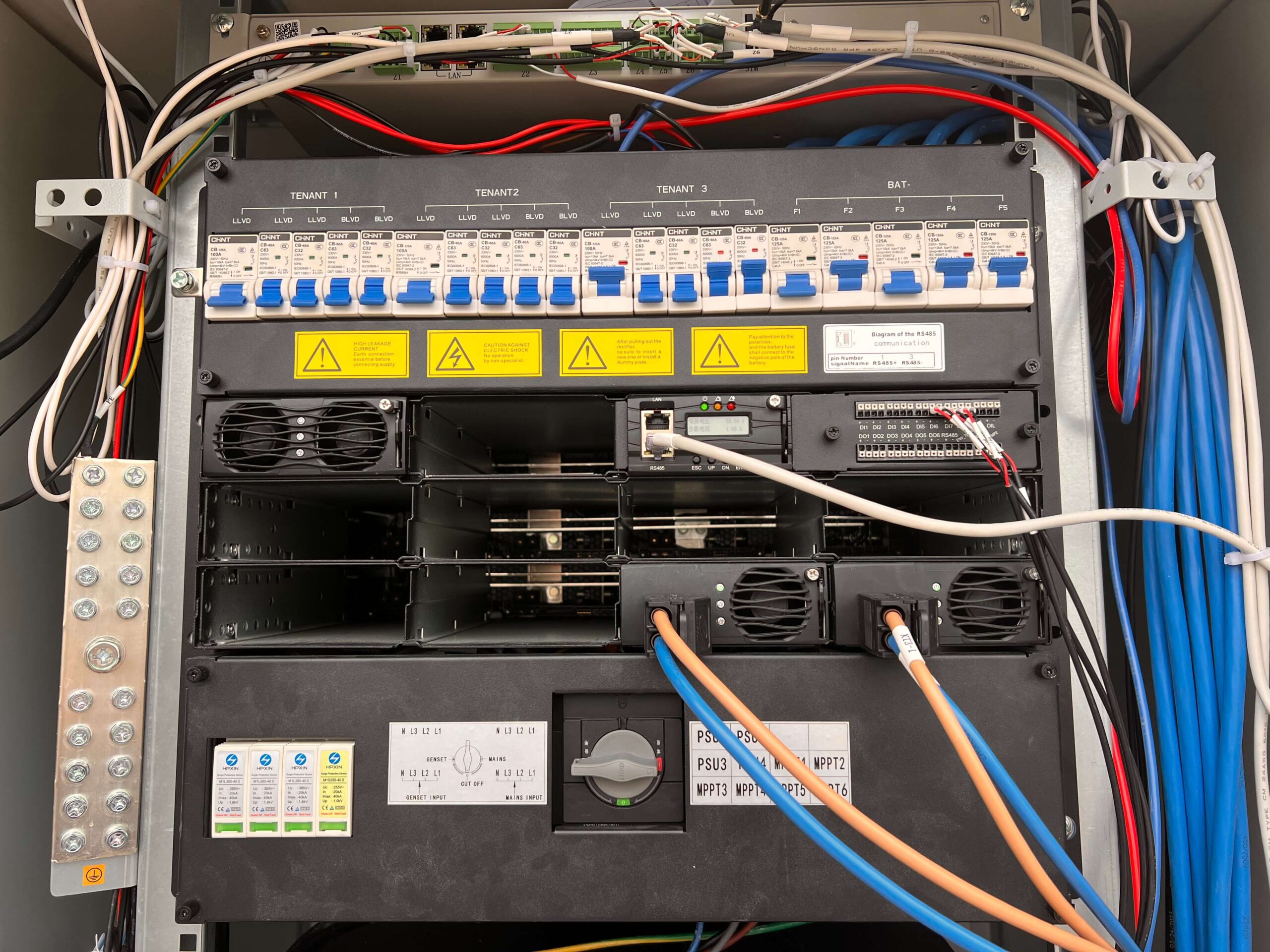
Telecom modules and outdoor network equipment accumulate small stack-up tolerances for each layer that can combine into an impedance shift large enough to affect high-frequency signal integrity. Their hidden BGA or QFN joints are exposed to thermal cycling that can cause them to fail.
Stack-up and impedance targets for telecom modules and outdoor network hardware are reviewed against the complete tolerance stack before fabrication. Coupon or TDR verification is also included when specified for the order, and hidden-joint inspection is based on the thermal-cycling risk. Once the batch has been completed, it provides inspected hardware for later RF and system-level testing rather than replacing that testing.

Audio/Video Interface Boards
Audio/video interface boards used in cameras, amplifiers, and displays, as well as HDMI interface boards, can have a small gap in shell grounding that passes a continuity test but still introduces EMI into the analog or high-speed signal path. The resulting noise may become apparent only once the board is inside the enclosure. Quick-turn manufacturing processes include checking the ground connection against this coupling risk, as well as verifying paste transfer and connector position.
The completed audio/video interface boards provide the basis for customers to conduct interface tests in their systems before product-level EMC testing.
Semiconductor Evaluation Boards
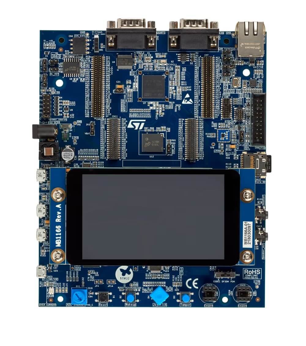
Evaluation and test boards designed for use with BGA or ASIC packages utilize sockets, which can produce variations in contact resistance between insertions. As a result, this contact-resistance variation may prevent the silicon engineering team from accurately evaluating the semiconductor’s characteristics. The quick-turn assembly process checks socket seating and contact consistency. This method also helps prevent the PCB from becoming a source of noise in the silicon team’s measurements.
From Prototype to Volume Production
Production quantity may increase only after the previous production stage has been validated for its intended purpose.
Quick-Turn PCB Prototypes
Prototype PCB designs are typically developed to answer a small number of targeted engineering questions or problems. The prototype should provide a sufficient quantity of boards to evaluate the engineering function, perform potential rework, and, if necessary, conduct destructive failure analysis. Ordering additional boards before establishing whether a change to the design or BOM is necessary would provide little value.
Pilot and Mid-Volume PCBA
Pilot and mid-volume runs check whether the same BOM, panel, stencil, machine program, soldering sequence, inspection limits, programming version, and FCT results repeat across more than one setup or batch condition. It is critical that any variance in BOM or firmware versions be clearly identified because the same PCB may be manufactured using multiple versions. The next quantity increase will be justified once all test results are verified as repeatable under the targeted manufacturing condition.
High-Volume Transition
The transition to high-volume PCB assembly requires a shift in focus from the speed of learning to the reliability and capability of the systems used to produce the boards. The accepted designs, BOMs, panels, stencils, fixtures, programs, test limits, traceability, packaging, and approved change processes should be established before scaling to volume production. Prototype exceptions, temporary substitutes, manual workarounds, and provisional test methods should either be closed or explicitly controlled before they are multiplied across production.
Our PCBA Production Lines
















Frequently Asked Questions
You may begin a quick-turn project with a quantity of one. The practical quantity depends on the stencil or fixture used, PCB complexity, the engineering purpose, and the current production stage.
Yes, as long as verified stock exists at the time of the order or a compatible substitute is authorized by the design team. Once verifiable material is no longer available, the order cannot continue until an alternative to the obsolete component is designed and approved.
Yes. Controlled impedance requires identification of the stack-up, target, tolerance, material, and verification method before quick-turn manufacturing. Via-in-pad prototypes require the filling, capping, drill structure, and added fabrication cycle to be identified before the board is scheduled for production.
Yes, as long as the products are being produced for development, qualification hardware, or pilot production in accordance with the applicable QMS, including traceability, recorded inspection limits, and inspection records. Qualification for the specific product remains the customer’s responsibility.