Upload BOM & Gerber
-
Mobile: +86 13312967631
-
Email: sales@sugaintl.com

IoT PCB Assembly Supplier
SUGA manages the assembly details that affect wireless performance, sensor accuracy, battery life, and traceable test results.
Coordinate PCB fabrication, sourcing, SMT/THT assembly, RF-aware inspection, programming, and functional verification for connected devices.
01005 Component Support
2.0 mil / 2.0 mil Line/Space
100 nA Sleep-Current Measurement
245–260°C Lead-Free Reflow Peak
What Is IoT PCB Assembly?
IoT PCB Assembly is the management of the controlled transition of a connected device circuit design into a populated, programmed, and verified board. An IoT PCB Assembly is the combination of PCB fabrication readiness, component sourcing, solder paste printing, placement, reflow, through-hole assembly as required, inspection, programming, and functional approval. The board in an IoT device may carry all of the following: wireless, sensing, power, and identity functions.
Wireless layout, sensor cleanliness, low-power states, identity data, and enclosure design impact what has to be controlled and documented.

IoT Assembly Coverage
The assembly may cover SMT and THT manufacturing, mixed-technology connectors, RF modules, sensors, secure elements, fine-pitch packages, cleaning, selective coating, serialization, and FCT fixtures. The processes used will depend upon the actual BOM, stack-up, component limitations, quantities produced, and testing requirements.
How IoT Modules Shape PCBA Architecture
When an IoT PCBA has been designed, the decisions made regarding how the PCB assembly will be built have an impact on much more than just the BOM. The PCB assembly decisions made will also affect placement density, antenna clearance, power states, programming access, inspection visibility, and test requirements associated with each board prior to releasing it for production.
Core Building Blocks Inside An IoT PCBA
The core building blocks within an IoT PCBA are shown. The following mapping of the board role, manufacturing concern, and validation output will keep those three elements connected.
| Module | Board role | Assembly concern | Validation output |
|---|---|---|---|
| Microcontroller / SoC | Data processing, device control, protocol handling | Fine-pitch placement, firmware access, thermal exposure during reflow | Programming result, boot check, functional sequence |
| Wireless communication module | Wi-Fi, Bluetooth, Zigbee, Z-Wave, cellular, LoRaWAN, NB-IoT connectivity | Antenna clearance, module placement, shield / ground control | RF registration, signal check, communication loop |
| Sensors | Temperature, humidity, motion, light, pressure, environmental input | Orientation, cleanliness, thermal sensitivity, analog noise | Sensor reading verification |
| Power management | Battery charging, regulator, power switch, energy harvesting, low-power MCU support | Leakage, sleep current, thermal profile, polarity | Current measurement and load state check |
| Memory | EEPROM, Flash, SD card, firmware / data storage | BOM lifecycle, programming, solder integrity | Read / write or boot verification |
| Interface components | USB, Ethernet, display, serial communication, board-to-board | Connector alignment, mechanical load, ESD path | Interface FCT |
| ADC | Converts analog sensor signals into digital data | Noise path, ground reference, sensor interface routing | Sensor input and signal conversion test |
| Security components | Secure element, authentication chip, tamper detection | Key provisioning, traceability, debug-port handling | Provisioning / identity check |
| Passive components | Resistors, capacitors, inductors, crystals | 0201 / 01005 placement, tombstoning, thermal balance | AOI / electrical check |
| Connectors | Pin header, USB, RJ45, wire-to-board, board-to-board | Insertion load, solder joint, clearance | Mechanical and continuity check |
How Device Type Changes Assembly Risk
Different product classes concentrate risk in different places. Cost figures below are planning ranges, not quotations.
| IoT Device Type | Typical BOM Cost | Primary Assembly Challenge | Critical Test Requirement |
|---|---|---|---|
| BLE/Zigbee sensor tag | $2–$10 | Sleep current leakage, antenna keep-out enforcement | Sleep current to ≤150% of target |
| LoRaWAN / NB-IoT node | $6–$30 | Module placement, thermal profile for modem IC | RF registration, sleep current |
| Wi-Fi + BLE combo | $5–$20 | Coexistence — shielding effectiveness | RF performance both bands, coexistence |
| Cellular gateway / hub | $20–$100 | Mixed THT + SMT, thermal management for cellular modem | FCT across all interfaces |
Low-Power Parts That Change Assembly Risk
Electronics include low-power components that impact assembly-related risk in IoT PCB assemblies. Low-power-based assemblies can support high manufacturing yields; however, poor placement or excessive leakage can have detrimental effects on performance and manufacturability.
Module Versus Discrete Radio Decisions
Due to the wide variety of applications within the RF front end, choosing a module can reduce RF design complexity and may provide prior approvals that come along with it. However, although a module may provide some previous approval from another manufacturer, considerations surrounding placement, antenna region, grounding, firmware, and integration should all remain under control of the OEM; the use of a module provides less opportunity for optimisation than that of an entirely discrete solution.
Where Wireless Interfaces Change Assembly Control
Integrating wireless interfaces into assemblies means that physical assembly choices will also affect RF performance. For example, changing the physical placement, creating ground discontinuities, and using different coatings or residues could alter the results of an assembly, even though the schematic itself remains unchanged. In the case of a particular implementation, such as an NB-IoT antenna, it should be validated in the physical environment in which it is intended to be used, rather than based solely on the design provided by the schematic.
Wireless Protocol Choices Affect Board-Level Assembly
Each protocol used with wireless devices will have a variety of influences on how circuits are designed and manufactured and what elements will be included as part of production.
| Protocol | Range | Data Rate | Power Consumption | Best For | Assembly note |
|---|---|---|---|---|---|
| Wi-Fi | 50–100 m typical indoor range; environment-dependent | Up to 1 Gbps by implementation | High | High-bandwidth, always-powered devices | Prioritize antenna clearance, RF path, thermal budget and coexistence. |
| Bluetooth LE | Device / PHY / antenna / environment dependent | 1–2 Mbps | Low | Wearables, proximity sensing | Watch low-power current, compact antenna area and shielding interaction. |
| Zigbee | 10–100 m | 250 Kbps | Very Low | Smart home, mesh networks | Keep module placement consistent across mesh device variants. |
| LoRa | 2–15 km | 0.3–50 Kbps | Very Low | Long-range sensors, agriculture | Long-range nodes need RF registration, enclosure and antenna validation. |
| NB-IoT | Cellular coverage dependent | Low-throughput; module / carrier / coverage dependent | Low | Wide-area IoT, remote monitoring | Modem IC thermal profile, SIM / eSIM identity, RF registration, and sleep-current state become production checks. |
| Thread | 10–100 m mesh range; environment-dependent | 250 Kbps | Low | Smart home, Matter ecosystem | Similar smart-home assembly risk to Zigbee; Thread 1.4 / Matter onboarding makes identity and provisioning control important. |
| Wi-Fi HaLow (802.11ah) | Up to 1 km+; link-budget dependent | 150 Kbps to roughly 78 Mbps class, depending on channel width and implementation | Moderate | Smart buildings, outdoor IoT | Outdoor / building devices may combine RF control with coating and enclosure checks. |
Antenna Keep-Out Is A Manufacturing Control
Antenna keep-out zones are more than simply a reference on the layout. The keep-out zone should also apply to fixtures, rails, labels, fasteners, batteries, shields, and rework of the board. The first-article review must confirm that the populated board has been processed and the method of production handling is consistent with the approved geometry. A communication check is recommended to identify serious issues in the design. However, before enclosures are completed, an enclosure-level antenna performance check must be performed on the completed product.
Shielding Cans Need Continuous Ground Contact
A shielding can is effective only if the frame, solder joints, ground path, and lid engagement match the design intent. An inspection of the can should look for coplanarity, paste deposit measurements, solder continuity, and any hidden components under the can prior to sealing. If access will be limited, the process must define whether the results of the inspection will be from AOI, X-ray, or staged inspection.
Flux Residue Can Become An RF Issue
Residue near a high-impedance node, between RF matching networks, and in a shielded region may introduce leakage or unstable operation. Factor in flux chemistry, component limitations, coating requirements, and environmental conditions when making the choice to clean or not to clean. A visual appearance check does not substitute for a defined cleanliness process when low current or high-frequency operation is sensitive to contamination.
Cable Routing Can Invalidate RF Assumptions
Power leads, display flexes, coaxial cables, and harnesses may couple into antennas or may alter ground return paths. Board testing should use a documented configuration of cables and connectors when those items show potential to alter the RF characteristics of the PCB. If production cable routing differs from the cables and connectors that were evaluated during testing, all prior assumptions made about the PCB's RF characteristics when it was tested for range, coexistence, or emissions may no longer be valid.
Which PCB Materials Fit IoT Operating Conditions
PCB materials for IoT applications should be selected based on RF behavior, thermal exposure, flexing, moisture exposure, thickness, and fabrication controls. In practice, the factors of flexing and RF loss sensitivity will narrow the selection of materials very quickly: a design requiring a bend will eliminate standard FR-4 from consideration, and a design that contains RF-sensitive paths at higher frequencies will eliminate laminates with higher dielectric losses from consideration, regardless of other material selection criteria for the application. A custom IoT PCB should not automatically have maximum performance capability; the selected stack-up should match the exact design, and the process conditions should match those of the defined process window.
Which PCB Parameters Need Project Verification?
| IoT Manufacturing Parameter | Standard Capability | Advanced IoT Option | Condition to verify |
|---|---|---|---|
| Min Line Width / Spacing | 3.0 mil / 3.0 mil | 2.0 mil / 2.0 mil | Copper weight, stack-up, yield target, supplier process window. |
| Microvia Diameter | 0.10 mm laser | 0.075 mm high-precision | HDI stack, via reliability, plating and inspection result. |
| Core Materials | FR-4 High Tg, Polyimide | Rogers / PTFE, Arlon Low Dk / Df | Thermal, RF, flexing, enclosure and cost conditions. |
| Fine-pitch IC placement | 0.35 mm pitch | 0.25 mm pitch | Stencil design, placement accuracy, AOI / X-ray accessibility. |
| Small passive package support | 0201 | 01005 | Feeder setup, stencil aperture, placement accuracy, tombstoning risk and AOI accessibility. |
| Impedance Control | ±10% standard | ±5% RF optimized | Coupon, test method, RF path geometry and laminate control. |
| PCB Finish | ENIG, OSP | ENEPIG / Soft Gold for wire bond | Fine-pitch, wire bond, shelf life and contact requirements. |
Which PCB Material Fits The IoT Design?
FR-4 suits many rigid sensor nodes, hubs, and controllers. Polyimide supports flexing and thin wearable or medical form factors, but moisture handling and assembly support become more important. Rogers or PTFE laminates may be selected for controlled RF loss, while ceramic can serve specialized thermal or high-frequency conditions. Hybrid constructions require attention to different expansion and processing behavior.
| Property | FR-4 | Polyimide |
|---|---|---|
| Flexibility | Rigid | Highly flexible |
| Dielectric Constant (Dk) | 4.0–4.4 | 3.2–3.5 |
| Thermal range to verify | 130–140°C class where FR-4 datasheet allows | 260–300°C material / process exposure where polyimide datasheet allows |
| Cost | Lower | Higher |
| Moisture Absorption | 0.1% | Up to 2% |
| Typical Thickness | 0.8–1.6 mm | 0.05–0.3 mm |
| Best Applications | General IoT, fixed installations | Wearables, medical devices, space-constrained designs |
Layer Count Should Follow Routing Density
| IoT board condition | Layer planning range | Main risk if under-layered |
|---|---|---|
| Simple Bluetooth sensor node | 2 layers may work; 4 layers is more comfortable | Ground return, EMI, RF margin and routing congestion. |
| Wi-Fi device or moderate digital complexity | 4–6 layers typical | Antenna path, power integrity and coexistence become harder. |
| Multiple RF paths, complex power, high-speed interfaces | 6–8+ layers common | Re-spin risk, EMI failure and test instability increase. |
| Dense HDI / fine-pitch IoT board | 4–8 layers with microvias, blind / buried vias and AOI / X-ray access | Via reliability, BGA visibility, impedance control. |
| Advanced HDI capability | Up to 32 layers; any-layer HDI up to 24 layers; 0.10 mm laser microvia; 0.25 mm microvia pad; stacked microvia up to 4 levels; 0.15 mm mechanical drill | Verify stack-up, via structure, reliability data, and project yield against the actual design. |
A board carrying RF paths alongside high-speed digital signals in the same stack-up commonly needs one or two additional layers purely for isolation between them — that added isolation demand, more than the device category itself, is usually what pushes a design into the next layer-count bracket.
When Thin Or Flex Boards Change Assembly Risk
For any ultra-thin or flexible circuit, there are additional assembly risks associated with its assembly. These risks involve panel support, controlled bend areas, defined stiffeners, connector reinforcement, and handling rules for the boards. In addition to the above-mentioned handling rules, component placement must avoid dynamic bending zones, and any circuit built with an ultra-thin or flexible substrate may also require an additional moisture conditioning step prior to the thermal process. The production documentation for circuits built with ultra-thin or flexible substrates should contain information regarding finished thickness, finished bend condition, stiffener geometry, coverlay openings, and inspection methods so the production process is consistent with the mechanical design.
How IoT PCB Assembly Moves Through Production
An IoT PCB manufacturing service can provide repeatability when the process is formed around design inputs, process controls, and testing.
- DFM / DFA and fabrication release: Before fabrication release, the Gerber files, BOM, assembly drawing, and testing requirements must be validated to ensure that the layout, antenna, package, stencil, test access, and readiness for board build have been validated.
- SMT setup: The setup of the stencil, feeders, and machine programming is based on the BOM, centroid data, and panel data. Other activities during SMT setup may include SPI setup, as required, and approval of the first part produced.
- Reflow: The reflow profile targets for the PCB and components have limits based on thermocouple profiling, soldering processes, component limits, and AOI / X-ray triggers where required.
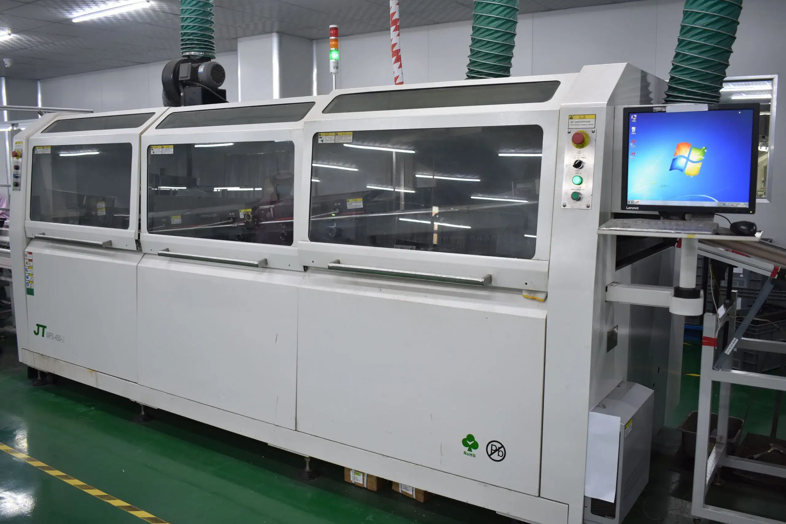
- THT / connector assembly: The THT / connector assembly process consists of assembly drawings and connector specifications that identify whether soldering will be done using selective soldering or wave soldering and whether solder inspection will be performed after the soldering process.
- Cleaning / coating: RF or environmental requirements must be defined to determine which washing, coating, masking, potting, and related inspection activities will be performed on the assembly where required.
- Programming preparation: Before the test program, the preparations made for programming an IoT PCB consist of the requirements for both the firmware and ID, which will define access, station planning, and the programming step.

DFM Review Before Fabrication
Before fabrication, the DFM review is an examination of the stack-up, antenna clearance, component orientation, package escape, stencil needs, panelization, fiducials, test points, and any mechanical constraints that may exist. The BOM review should flag lifecycle, alternates, moisture sensitivity, and programming requirements to address these items before fabrication, thus ensuring both yield and the continued validity of any testing performed after fabrication.
How Fine-Pitch Placement Is Controlled
Fine-pitch ICs, 0201 passives, and 01005 passives require equivalent alignment of stencil apertures, board support, feeder setup, placement accuracy, and inspection access to ensure a successful assembly process. Use of SPI before the component is placed can help to identify any deposit issues before the components are obscured on the board. The first-piece approval process should confirm polarity, orientation, marking, offsets, and the correct revision before all components in the lot proceed through the assembly process.
Lead-Free Reflow For Heat-Sensitive IoT Parts
The peak reflow temperature for lead-free solder is typically considered a reference point at 245–260°C, but actual profiles will differ according to solder-paste guidelines, component temperature limits, board thermal mass, moisture sensitivity, and where thermocouples are located on the board. There are specific limits for radios, sensors, batteries, plastics, and specialty laminates that may be more restrictive than general leaded and leadless components. The measured profile must be stored to create a direct link to the thermal exposure received by the released assembly lot.
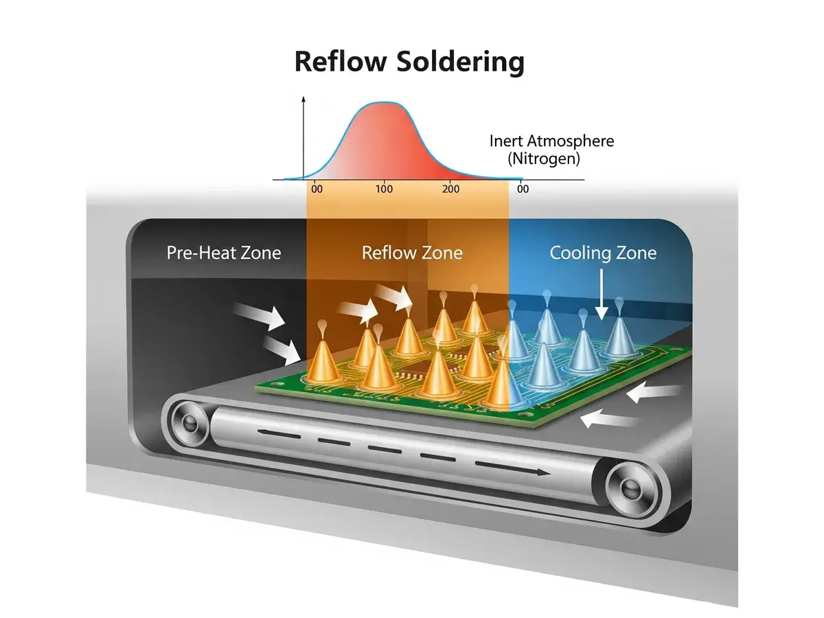
Mixed SMT / THT Assembly
Typically, gateways, controllers, and similar products will have both dense SMT assemblies and headers, relays, terminals, large connectors, and in some cases, SMD components. The assembly process must account for solder access, a secondary heating cycle, component shadowing, mechanical support, and insertion force. Selective soldering or wave soldering processes must protect adjacent SMT parts while still allowing for inspection of completed solder joints.
How Protection Steps Affect IoT Boards
Cleaning and coating processes are based on flux type, RF sensitivity, leakage requirements, humidity control, contamination control, and service conditions for the assembly product. All of these processes require consideration of material compatibility, masking, thickness control, cure, and inspection procedures. The addition of potting adds thermal and potential rework issues to these processes. As such, care must be taken to ensure that none of these processes cover test points, detune antennas, trap residues, or impair connectors — for example, a conformal coating applied too close to an antenna edge can shift its tuned frequency far enough from the original frequency to prevent a successful communication check when tested.
Programming Preparation Before Test
Programming preparations must include both firmware and access methods, as well as how the operations are to be controlled. Serial numbers, MAC addresses, UUIDs, or credentials must all remain unique and be able to be traced back to the assembly lot. Debug access for tooling should follow the product security protocols while enabling production.
Which Tests Prove IoT PCBA Readiness
No single inspection can prove that a PCBA is ready. The testing of IoT PCBs should include a system of testing based on hidden solder, powered operability, wireless operation, low-current states, programming, and product shipment risk.
Inspection Methods Should Match Hidden Failure Modes
| Test / inspection | What it can show | IoT-specific trigger | What it cannot prove alone |
|---|---|---|---|
| SPI | Solder paste volume and alignment | 01005 / 0201, QFN, fine-pitch modules | Powered behavior, RF performance, sleep current |
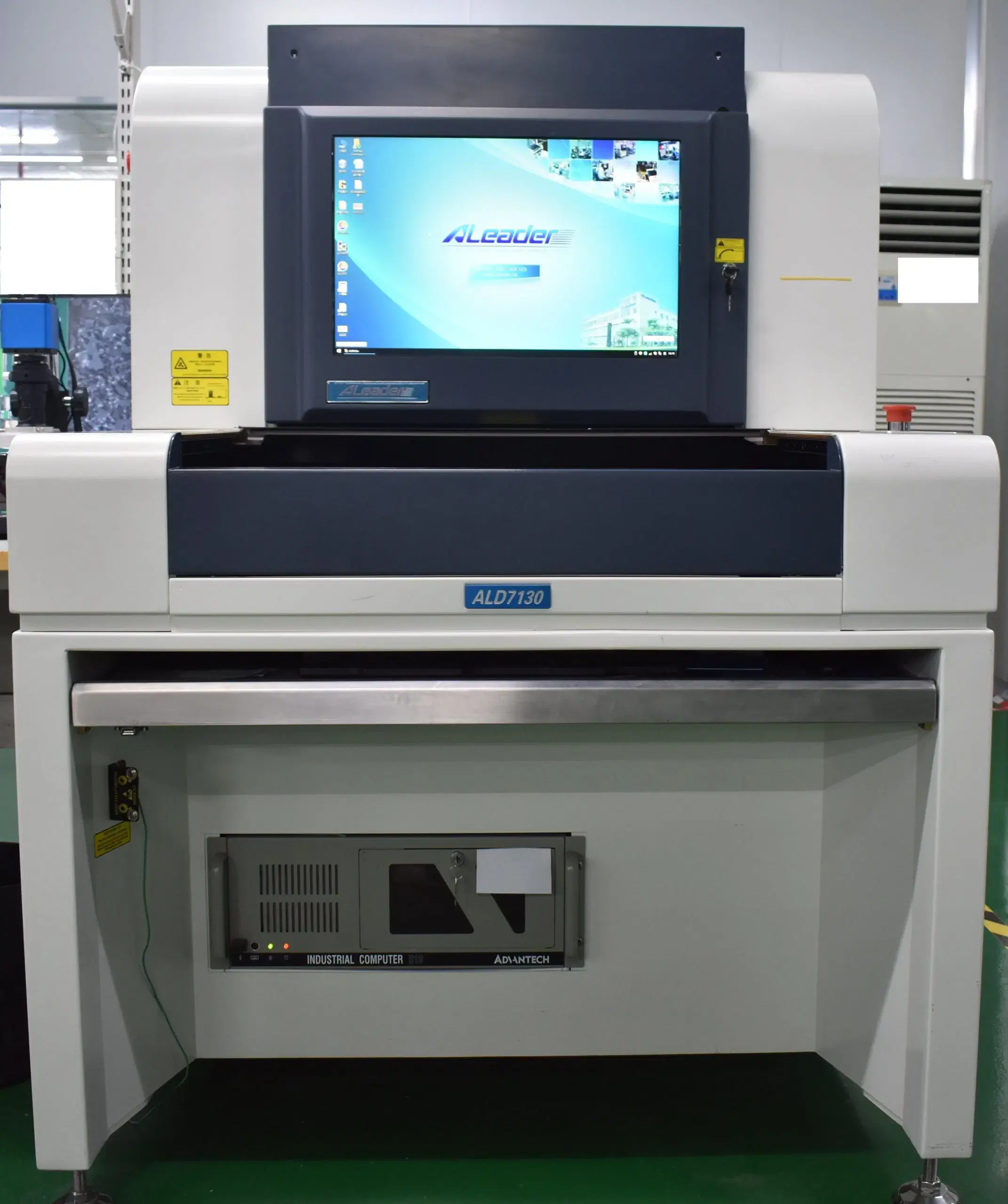
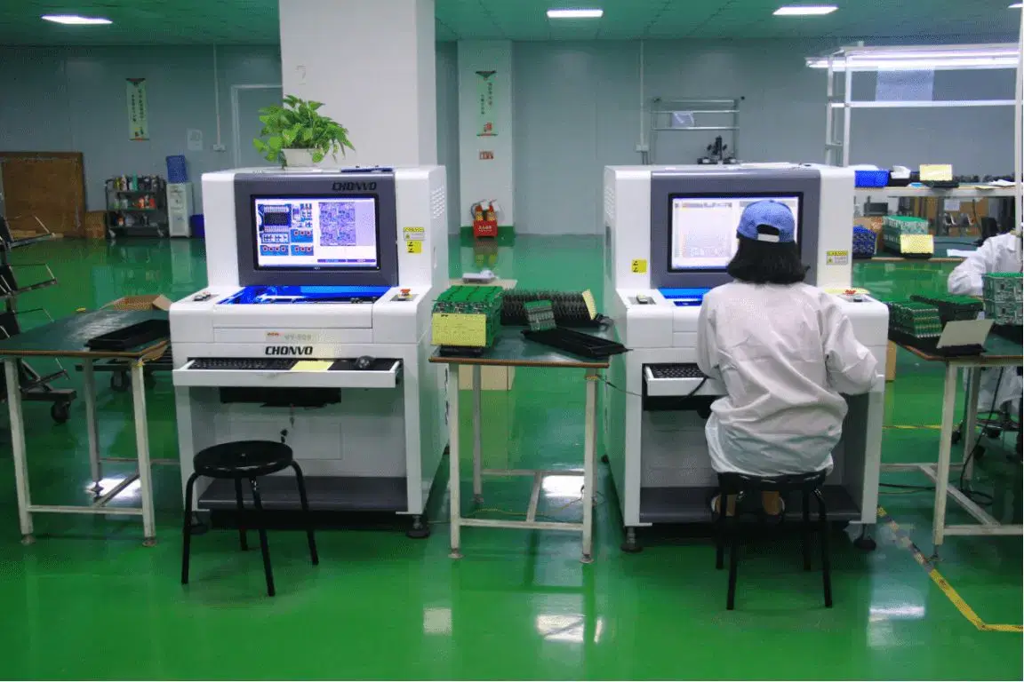
| AOI | Visible solder, polarity, placement, marking | Dense SMT and module assembly | Hidden BGA / QFN voiding, leakage current, RF detuning |
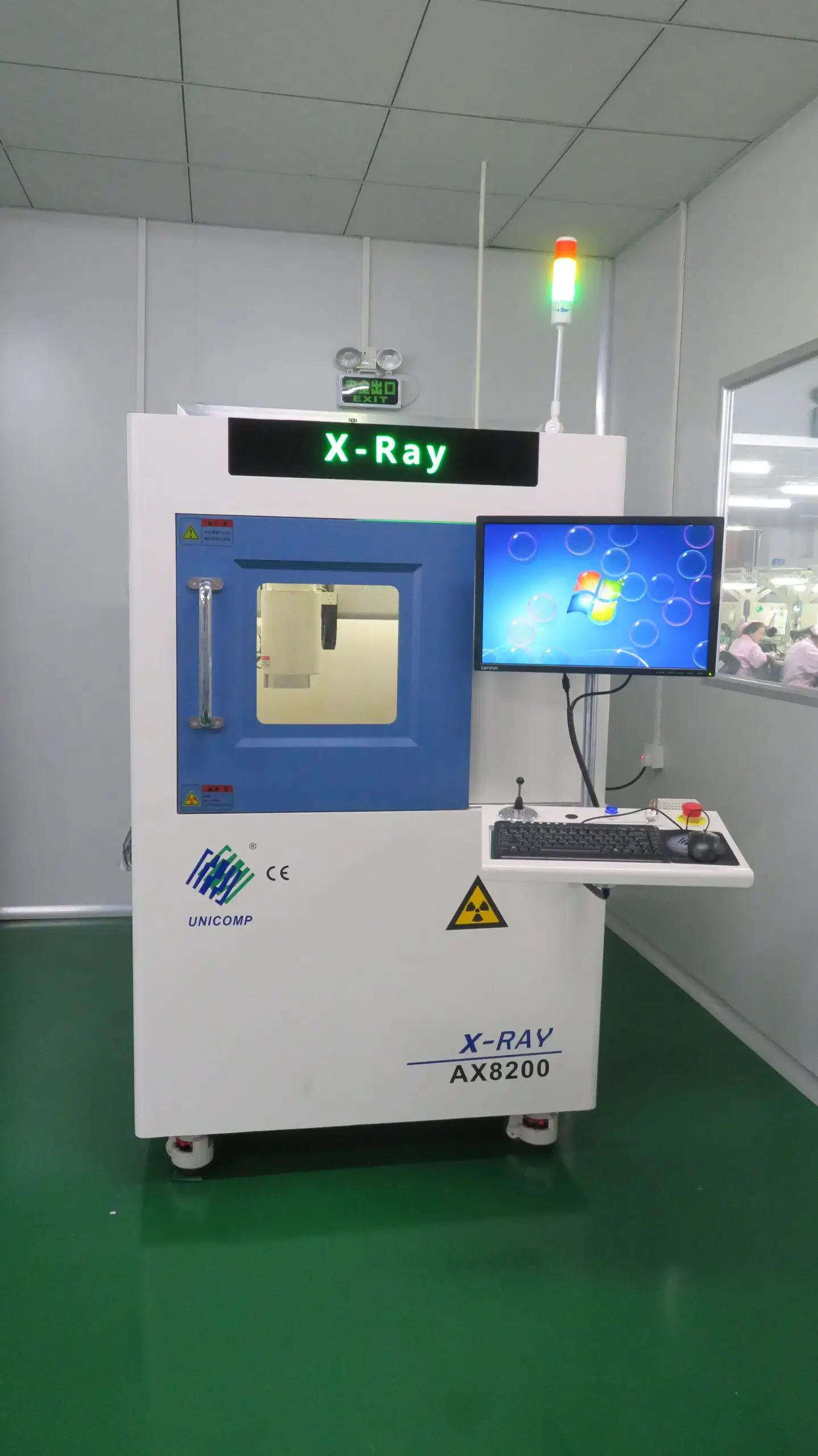
| X-ray | Hidden solder joints, BGA / QFN / voiding | BGA packages, QFN thermal pads, shielded areas | Firmware, sensor reading, wireless communication |
| ICT / flying probe | Electrical network and opens / shorts | Early build verification, no fixture or fixture-based checks | RF performance, sleep current profile, final device behavior |
| FCT | Powered sensor / interface / communication behavior | Gateway, sensor node, wearable, access control | Certification unless final product setup is tested |
| RF test | Output power, receiver sensitivity, return loss, range / communication loop | Wi-Fi, BLE, Zigbee, LoRa, NB-IoT, cellular modules | Battery life, material traceability, sourcing risk |
| Sleep current test | 100 nA-level current measurement capability when firmware state, fixture leakage, instrument resolution, sampling window and target limit are defined | Battery-powered IoT | Solder joint geometry, RF certification, final enclosure behavior |
| Programming / serialization check | Firmware, serial number, MAC, UUID, certificate / credential check | Cloud-connected devices | Hardware reliability unless paired with FCT |
Sleep Current Needs Defined Test Conditions
Boards can pass a fine test on a bench but can still fail in the field, depending on how the test setup is configured. Often, poor pogo-pin contact resistance at the fixture or an unpowered debug header terminal can introduce additional parasitic leakage in the order of tens of nanoamps, with some designs resulting in hundreds of nanoamps, which can lead to boards meeting all compliance requirements but being seen as out of spec.
To have confidence in the accuracy of a sleep-current measurement, four different conditions must be fixed. First and foremost, the firmware must be tested in the actual deep-sleep mode that is specified in the product's shipped firmware as opposed to using test firmware that is simply an idle loop. Second, the measuring instrument must have resolution below 100 nA, and it must allow settling time for several seconds or more at these current levels. Third, test fixtures should be characterized for their own baseline leakage before loading boards into the fixture. Finally, it is critical that the voltage provided to the board is representative of the actual voltage as it will be connected to the battery during operation and must track the actual discharge curve of the battery, since MCU leakage is voltage-dependent.
In addition, a test report of a board that has been tested at the 100 nA level is essential to confirm whether the board meets its intended ultra-low-power specification and to understand the project scope. Without these conditions and limitations when evaluating test reports for a given design, comparing test results across different board revisions cannot be consistently validated.
RF Test Should Match Production Configuration
RF testing should be conducted using the released RF module, the original antenna that was specified in the release, the original firmware version configured at the time of release, the same power state as the original design, the same cables used to connect the equipment, including any existing shields, and any other relevant environmental conditions that may impact performance. Depending on project risk, output RF test report information should include some combination of registration, communication loop performance, output power, receiver sensitivity, return loss, or range.
Programming And Identity Checks Are Part Of IoT Verification
Identity checks, along with the programming of connected components, play an important role in the verification process of IoT devices. It is important to ensure that all programmed data, such as firmware, serial identity, MAC address, UUID, certificate, or other credentials, are accurate, because even though a connected device PCBA is found to be electrically sound, if the data is incorrect, the device will not operate properly. Programming stations must implement appropriate controls to ensure that unique identifiers are assigned to each device, that test and programming information is properly recorded, and that any security information or components used in the project are handled in accordance with the project plan. A boot check or interface check is then used to confirm that the programmed data is valid for use.
Test Results Must Stay Tied To Lot And Revision
All test results should be associated with the appropriate lot and assembly revision for the purpose of documentation. Every test report should include all of the required fields, including the assembly revision, BOM status, firmware version, lot number, station used to perform the test, test limit, date and time of the test, and the result of the test. When a component, antenna, coating, enclosure, or firmware status is modified, it is critical that the test is assessed as to whether it needs to be repeated. The traceability of all test results helps ensure that passing test results are actionable instead of being isolated as a single screenshot or number.
IoT PCB Assembly Applications

Smart Home Devices
IoT devices that are commonly used in smart homes include items such as smart switches, thermostats, hubs, and appliances. Smart home devices usually consist of compact radios with either mains or low-voltage power, and have the advantage of user interfaces along with mechanical housing considerations. An IoT PCB supplier for smart home devices should make certain that the layout of their devices will provide the necessary space for the antennas, the proper separation of the antennas if applicable, the alignment of connectors, the programmed identity, and the necessary environment for all devices to operate simultaneously. The most common problems caused by using a metal housing or multiple antennas to coexist together, such as a Zigbee or Matter mesh coexisting in the same area as a Wi-Fi radio, are measured range losses that will not occur until after the housing and surrounding devices have been installed.
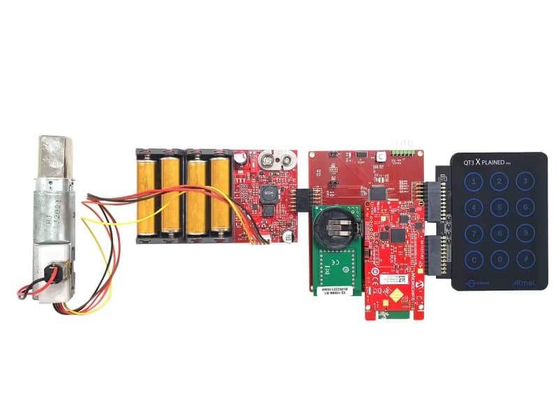
Smart Lock And Access Control
An IoT PCB assembly for a smart lock or access control device requires assurance of secure identity along with motor or relay loads, battery life, and reliable wireless connections. Testing for production should also include programming, current states, connectors and interfaces for sensors, and actuator response. If the power rails are not decoupled during the transient event, motor or relay inrush current on the same board with a low-power microcontroller unit can cause brown-out resets during actuator movement. This risk will only be captured by FCT if the actuator is physically under load during the test; otherwise, it is checked electrically only.
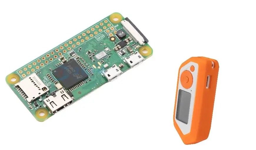
Industrial IoT Sensors
Industrial sensor nodes are subject to various forms of vibration, contamination, temperature fluctuations, long cable lengths, and noisy power supply lines. Assembly planning must accommodate the electrical connectors, sensor cleanliness, coating and protection if applicable, and communication checks. An enclosure or coating rating such as IP65/IP67, or a thermal cycling count, must be tied to a specific test method at incoming inspection; if the technical specifications are not tied to a verifiable method or cycle count, then they cannot be checked at the receiving line.
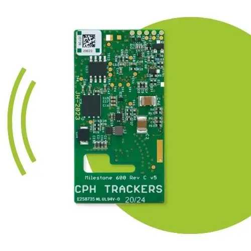
Asset Tracking And Logistics
Trackers frequently combine GNSS capabilities, cellular capabilities, motion sensing, compact batteries, and aggressive sleep states. Module placement, the environment surrounding the antennas, SIM or eSIM identity, serialization, RF registration, and defined sleep-current testing are critical to the production check process.
Wearable Devices
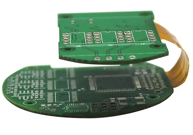
Wearable IoT PCBs combine radios, sensors, charging, and power management into a thin or flexible package. Moisture handling, support for bending, fine-pitch placement, low-current measurement, and mechanical integration need to be coordinated, as enclosure proximity and body proximity can affect how well the wireless system works.
Healthcare And Medical IoT
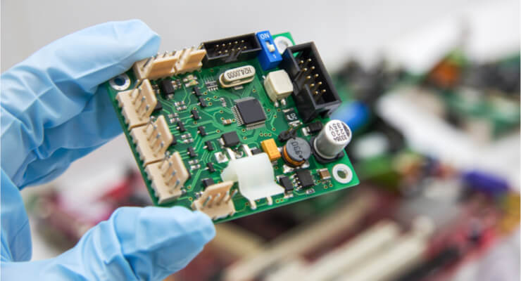
The assembly requirements for healthcare IoT products often involve elements that do not appear on the bill of materials for standard consumer products. The materials used in the construction of devices with patient contact are typically subjected to biocompatibility testing according to the ISO 10993 series. Devices with patient contact have strict requirements regarding materials and the way they are made because what is acceptable for coating or solder masking on a smart thermostat may be considered a rejection item on a wearable patch. The electrical safety of the device is usually evaluated against IEC 60601 series requirements, which dictate how creepage and clearance spacing is determined and can dictate whether the assembly requires an isolated power architecture that will change how the assembly is connected and how connectors and potting strategies will be used. Quality records of an assembly made into a regulated medical device usually trace into an ISO 13485 quality system and not just a general electronics quality management system, so there are additional requirements for traceability of lots, deviation records, and change control. The method of sterilization used for the finished device, such as autoclaving, ethylene oxide, or gamma radiation, will also impact the types of coatings and materials that can be used because conformal coatings that can survive reflow do not necessarily survive multiple sterilization cycles.
Agricultural IoT
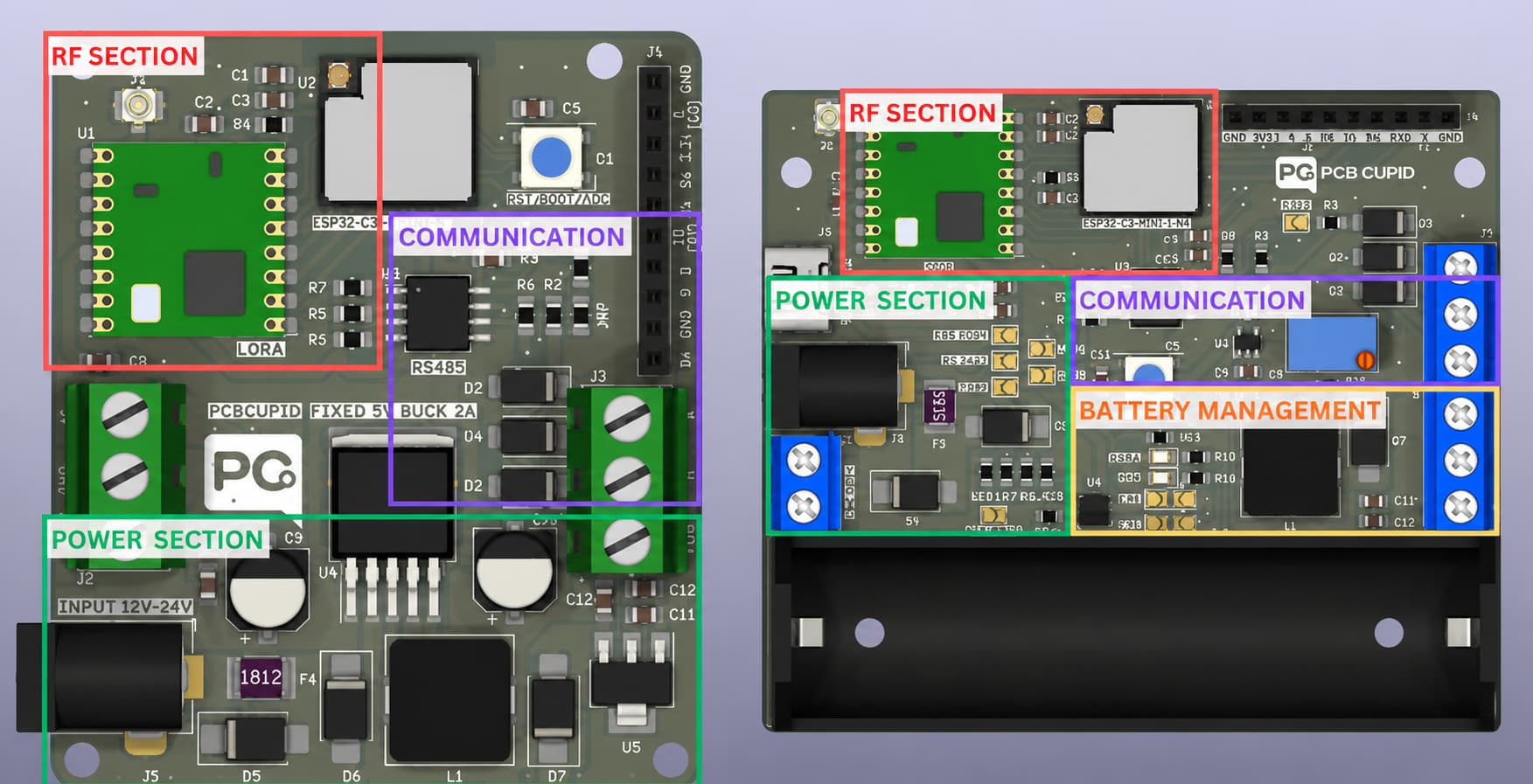
A PCB for agricultural IoT typically includes components for long-range communications, solar or battery power, sensing capabilities, and exposure to outdoor elements. The production control requirements for deploying an agricultural IoT PCB should include proper antenna configurations, sleep-current states, coating or sealing methods, proper handling procedures for connectors, and testing for proper communication in the deployed design. Solar charger designs require separate verification of cold-start charging and steady-state charging because a battery management IC that will charge effectively at room temperature may not start charging properly if the environmental temperature is below freezing.
Automotive And Transportation IoT
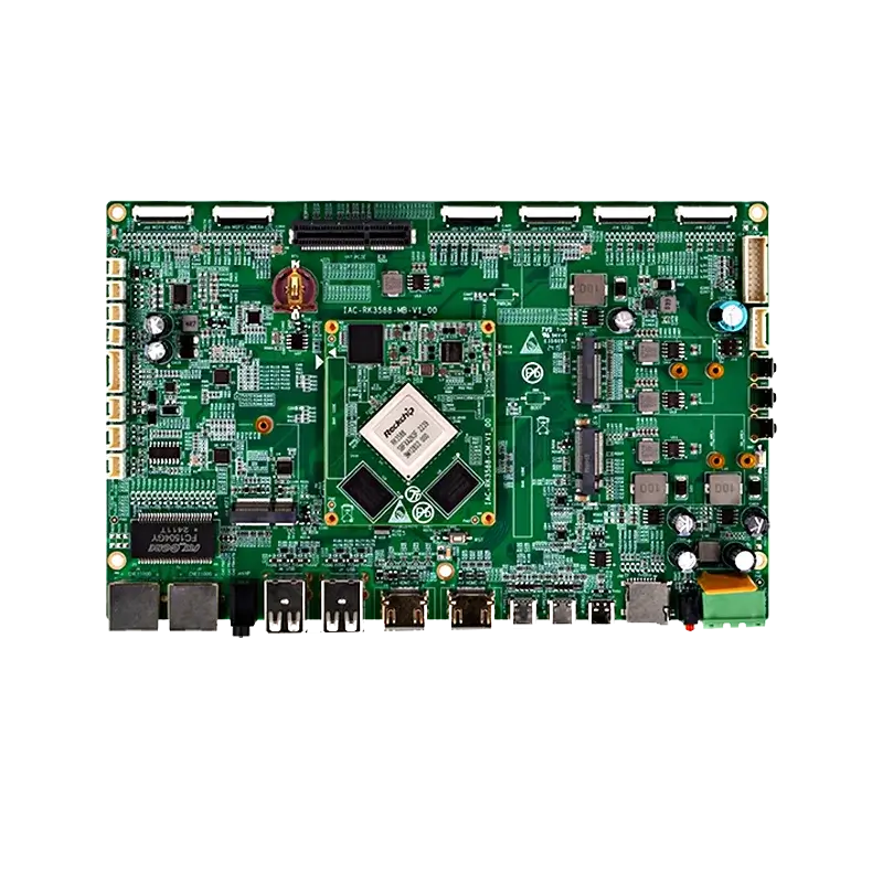
Fleet and transportation tracking devices may be exposed to environmental transients, vibration, temperature swings, cellular provisioning, and different interface protocols. Automotive-grade qualification, such as AEC-Q100 for ICs and AEC-Q200 for passives, is important for components in the sensing and power path because commercial-grade components can fail thermal cycling in a vehicle, even when they work perfectly fine in smart-home hubs. Environmental testing in this area is often benchmarked against ISO 16750 standards due to the wide temperature range, load dump, reverse polarity transients on the power input, and wide input-voltage tolerances that have to be validated at the assembly level, not simulated during design, because they are vehicle-side electrical conditions that do not exist in the schematics. Cellular modules used for provisioning need to be qualified with carrier certification before being committed to volume, because substitution of a module after certification can require another test cycle.

Smart City Infrastructure
Devices like lighting controls, meters, parking sensors, and public monitoring equipment need to have a long operational lifetime and repeatable field identity. Manufacturers are responsible for managing the environmental protection of their products, as well as wireless-module setup, connectors, firmware, serialization, and functional communication prior to the installation process. The operational life of these devices often spans many years; the risk of component end of life and spare-parts availability needs to be assessed before the design freeze rather than discovering the risk after the first field failure.
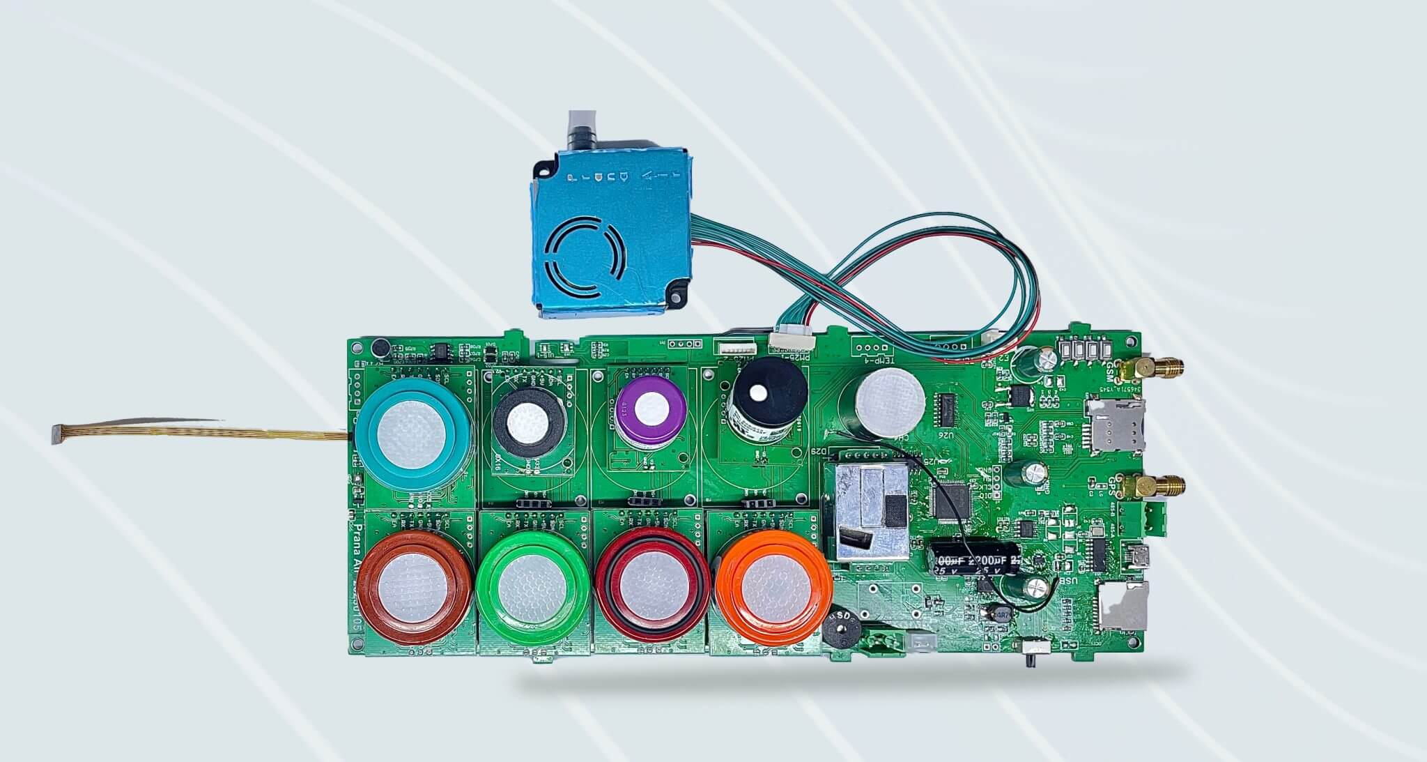
Environmental Or Remote Monitoring
Remote monitoring systems must place high importance on low power consumption, sensor integrity, long-range links, and resilience where maintenance is unavailable. Minimizing the risk to field systems can be achieved through clean assembly, precise sleep-current testing, and testing the antenna and enclosure, all of which help to mitigate preventable field risks. Measuring sleep-current drift over the entire temperature service range, which is a test that is separate from the room-temperature measurement, is essential to determine the actual limits of any performance guarantee at extreme operating conditions, as leakage current in low-power MCUs is temperature-dependent and the room-temperature test does not guarantee the same margin at the extreme operating conditions of the equipment in the field.
How Prototype Production Moves Into Volume Production
As the prototype moves into volume production, the dominant risks are going to change.
Volume Stage Changes The Cost Driver
The figures in this section are planning ranges and should not be assumed to be fixed quotes.
| Volume | Estimated Cost / Board | Primary Cost Driver | Most Effective Cost Lever |
|---|---|---|---|
| 50–200 prototype | $20–$100 | NRE, minimum order quantities | Avoid re-spins — get DFM right first time |
| 500–2,000 pilot | $5–$20 | Test fixture setup, certification | Invest in FCT fixture now — pays back immediately |
| 5,000–20,000 | $2–$6.5 | Component pricing, yield loss | BOM optimization, approved alternates |
| 50,000+ | $0.60–$3.50 | Component cost, line efficiency | Long-term component contracts, dedicated line |
Hidden Cost Layers In IoT Assembly
The figures below are planning ranges, not fixed quotations.
| Cost layer | Cost / Planning Figure | Where it affects planning |
|---|---|---|
| Regulatory certification amortization | FCC ID + CE mark + IC Canada: $14,000–$65,000 | Volume economics, module vs discrete choice |
| Certification per-unit effect | 5,000 units: $2–$15 / unit; 100,000 units: $0.2–$0.60 / unit | Business case planning |
| Selective conformal coating with UV inspection | $0.50–$1.50 / board | Outdoor, industrial, medical IoT |
| Firmware loading / serialization | $0.30–$0.80 / unit | Unique serial, MAC, UUID, cloud credential |
| Sleep current test time | 6–18 seconds / board; $1.50–$3.5 / board | Battery-powered IoT FCT |
| Aqueous cleaning | $0.2–$0.5 / board | RF boards above 2.4 GHz, shielded areas |
| EMC re-test risk | $4,000–$16,000 | RF / antenna / coating / enclosure changes |
| Safety stock | $3.50 module × 10,000 buffer = $35,000 | Working capital for long-lead wireless components |
Prototype Production Does Not Equal Volume Production
A hand-built prototype can confirm basic function while hiding feeder constraints, panel behavior, thermal variation, fixture leakage, inspection access, and sourcing exposure. Pilot production should use representative tooling and document deviations. Volume release requires stable files, approved components, repeatable stations, measurable limits, and a controlled response to failures.
What Proves The First Production Lot?
| Step | Production baseline action | Output |
|---|---|---|
| 1 | Assemble 10–20 units using production tooling: stencil, pick-and-place, reflow profile, selective wash | First production article lot result |
| 2 | Run full FCT including sleep current and RF performance | Functional / RF test report |
| 3 | Cross-section 2–3 boards | QFN thermal pad voiding, microvia barrel copper thickness, solder joint intermetallic formation |
| 4 | Run 50-cycle thermal shock −40°C to +85°C on 5 boards where reliability screening is required by customer specification | Reliability screening result when required |
| 5 | Document all results as production baseline | Sign-off before scale-up |
Sourcing Risk In Volume Production
Various electronic and radio components may include wireless modules, sensors, secure elements, and power parts, which may have long lead times or controlled firmware variants. It is necessary to evaluate each approved alternate against the following areas: size, footprint, electrical behavior, antenna configuration, software, lifecycle, and any applicable revalidation required for each component. All component lot traceability and safety-stock considerations must reflect the demand for each component, its risk, and available working capital.
Production Changes Must Match Certification Assumptions
Changes to any of the following production components, such as radio modules, antennas, PCB materials, layouts, shields, coatings, cables, enclosures, power supplies, or firmware, could potentially affect or invalidate any previous compliance assumptions that may have been made with respect to the original components used to obtain compliance. The change control process should reference the evaluated setup from which the changes were made and identify that a technical review must take place before the replaced parts are approved for use.
How To Choose An IoT PCB Assembly Supplier
Having a capability list on a supplier's website means very little without evidence to back up its claims. The supplier must be capable of producing project-level proof through actual test results, inspection records, and production method data associated with a real PCB for each statement in the following sections.
Supplier Proof Checklist
Maximum-capability lists need project-level proof.
| Proof area | What to check | Better proof |
|---|---|---|
| Engineering support | DFM / DFA review for antenna, package, stencil and test access; IoT failure often starts before production | DFM comments, risk list, layout feedback |
| Engineering support | RF-aware manufacturing review; wireless products are assembly-sensitive | Antenna keep-out check, RF path note, shielding / coating plan |
| Engineering support | Low-power review; battery life depends on cleanliness, component choice and firmware state | Sleep-current test plan and target limits |
| Engineering support | Programming / security review; IoT devices need unique identity and update path | Firmware version, ID provisioning, debug-port plan |
| Manufacturing capability | 01005 / fine-pitch claim; do not accept capability list alone | Actual package, pitch, inspection access and AOI / X-ray plan |
| Manufacturing capability | 2.0 mil / 2.0 mil claim; do not accept one-line max capability | Stack-up, copper, yield target and process window |
| Manufacturing capability | ±5% impedance claim; do not accept a marketing proof card | Impedance coupon, test result, RF stack-up and material traceability |
| Manufacturing capability | HDI / any-layer / stacked microvia claim; do not accept generic capability | Via structure, layer count, cross-section or microsection result |
| Manufacturing capability | Coating / potting claim; do not accept “Can do coating” alone | Material type, masking plan, UV inspection or coating result |
| Production testing | BGA / QFN / hidden solder | X-ray / AXI report or image sample |
| Production testing | Fine-pitch SMT | AOI record, first-piece inspection, SPI if required |
| Production testing | Battery-powered IoT | 100 nA-level measurement capability where required, plus sleep current target, fixture condition and measured result |
| Production testing | Wireless device | RF performance result, communication loop or first-article RF result |
| Production testing | Cloud-connected product | Firmware version, serial / MAC / UUID / certificate programming result |
| Production testing | Industrial / outdoor product | Coating / cleaning / environmental test result where required |
Traceability And Revision Control
Make it easy to trace the PCB lot, component lots if needed, BOM and assembly revision, firmware, programmed identities, test results, deviations, and final result. Also ask how records are accessed after shipment and how approved changes are obtained. This is important since the configuration provided by one antenna, firmware state, or coating process may not be valid for a different configuration.
Who Owns Component Sourcing Risk
Identify who assumes the sourcing risk for all components, such as who buys all parts, approves alternates, manages moisture-sensitive devices, checks authenticity and date codes, and owns shortage decisions for component orders. Acceptable proof of component sourcing risk would include approved vendor controls, incoming lot results, lot links, lifecycle alert notifications, and customer authorization to replace or substitute items. When sourcing wireless modules and security parts, the ordering code and programmed variant are just as important as the markings on the package.
What Standards Can a Supplier Support?
Standards should be connected to their actual use.
| Standard family | Current revision / use | Use limit |
|---|---|---|
| IPC-A-610J | Acceptability of electronic assemblies | Use only when customer-defined acceptance class applies; do not treat it as finished-product certification. |
| IPC J-STD-001J | Requirements for soldered electrical and electronic assemblies | Use for soldering process and workmanship requirements where specified. |
| IPC-A-600M | Acceptability of printed boards | Use for bare-board acceptability; do not mix it with PCBA solder-joint acceptance. |
| IPC-6012F | Qualification and performance specification for rigid printed boards | Use for rigid PCB fabrication where the board type and class require it. |
| IPC-6013E | Qualification and performance specification for flexible / rigid-flex printed boards | Use for flex and rigid-flex work where applicable. |
| IPC-7711/21D | Rework, repair, and modification procedures | Use for controlled repair / modification process support, not as permission for uncontrolled rework. |
| IPC/WHMA-A-620F | Requirements and acceptability of electronic wire harnesses and cables | Use only when cable, harness, or connector assembly is part of the project work. |
An assembly supplier can support test results, samples, and change control for a compliance program.
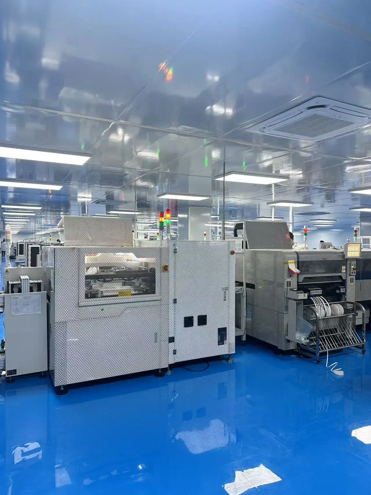
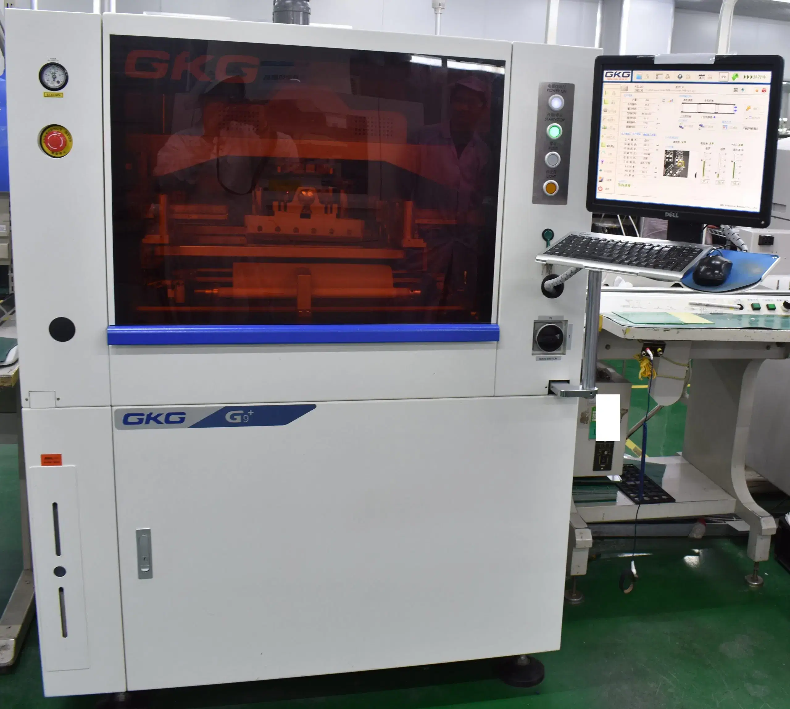
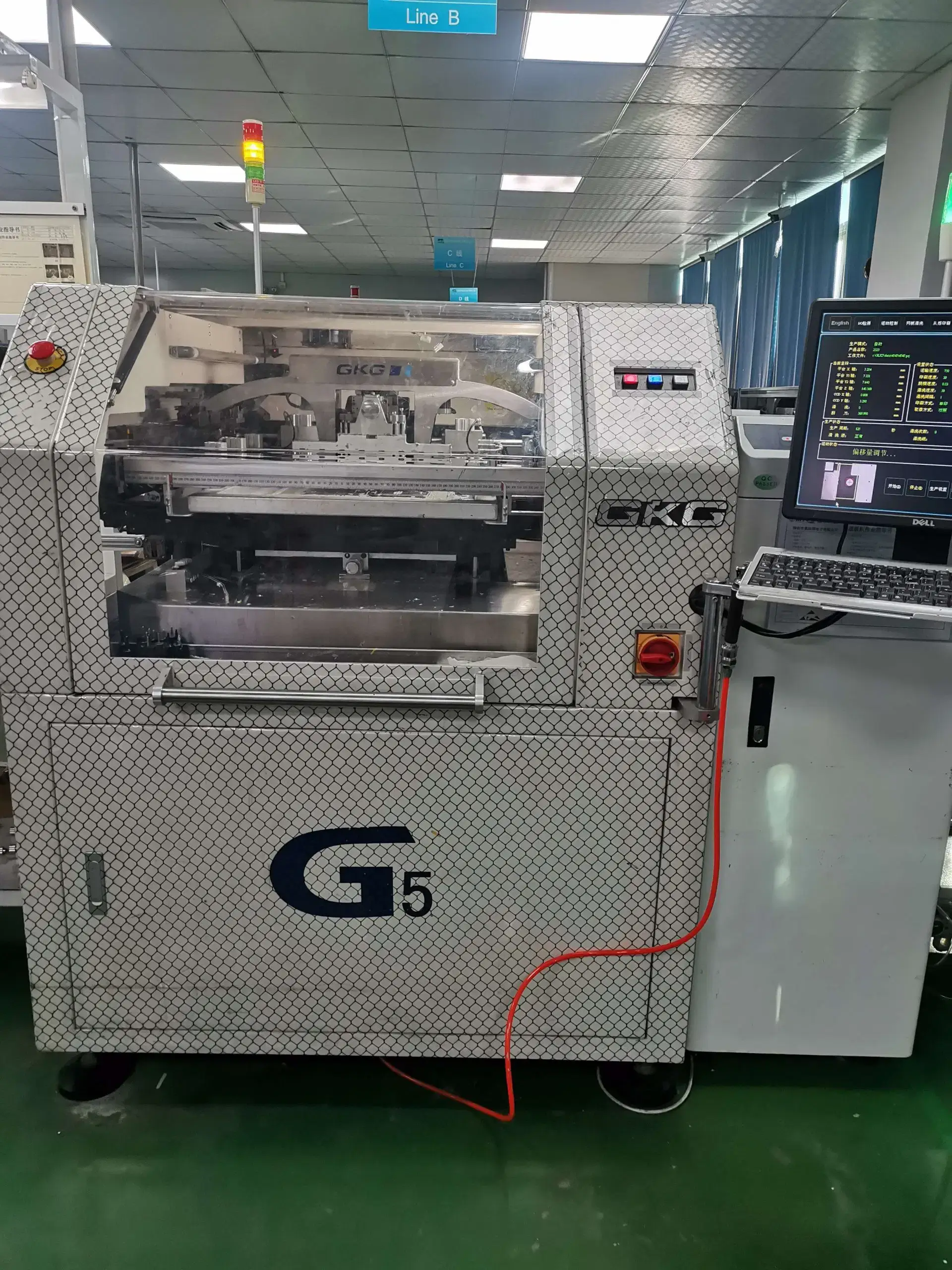
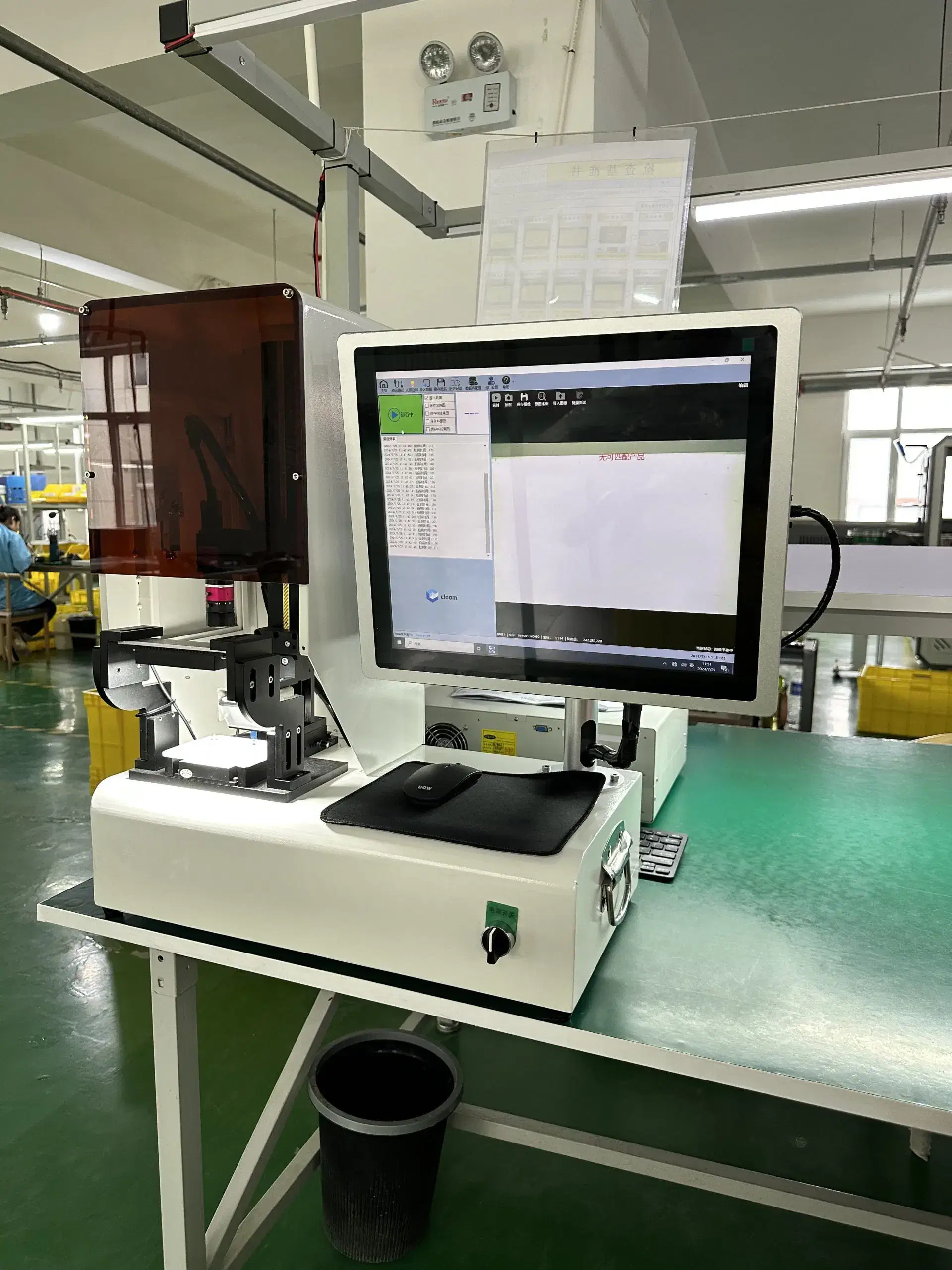
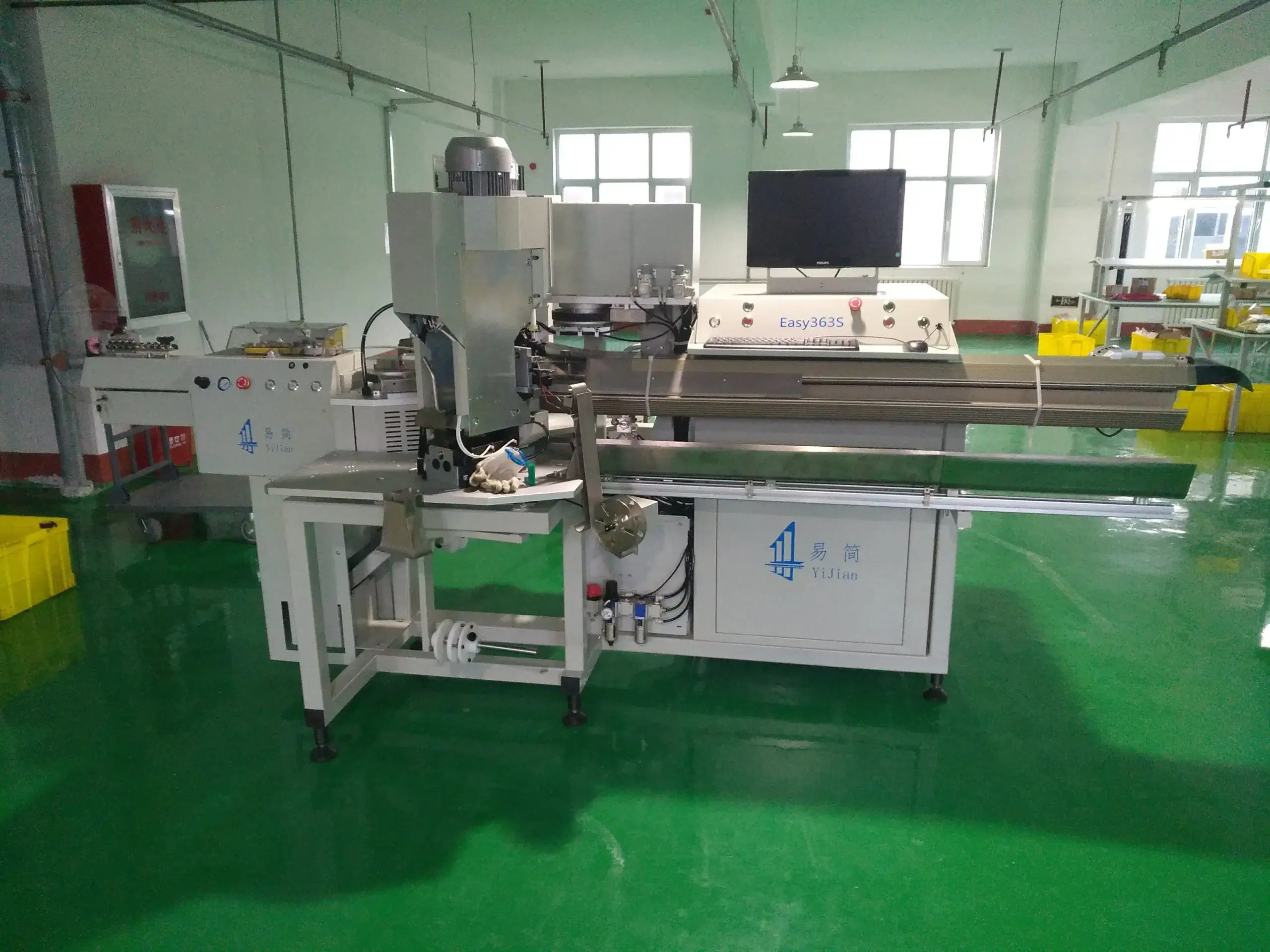
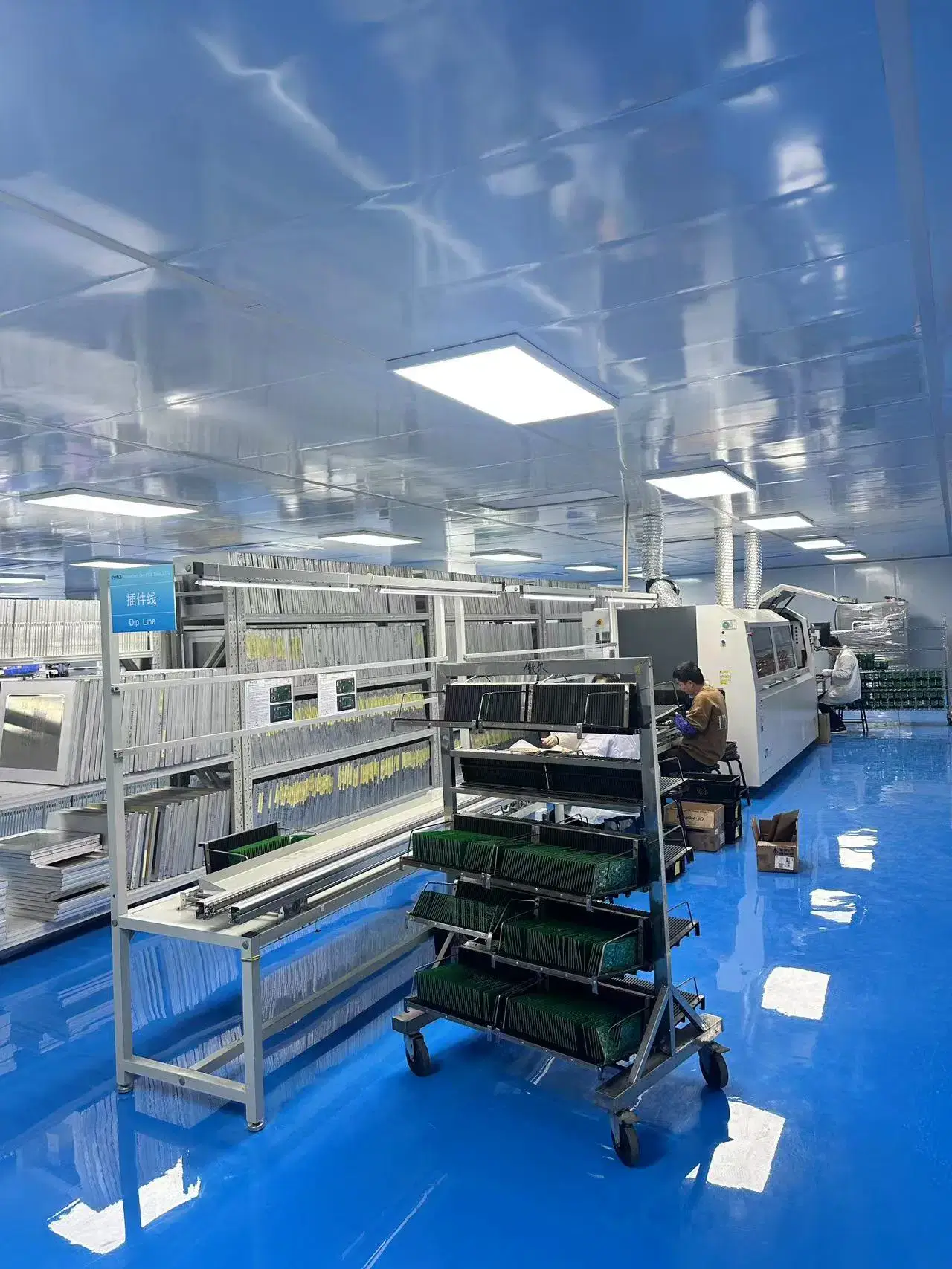
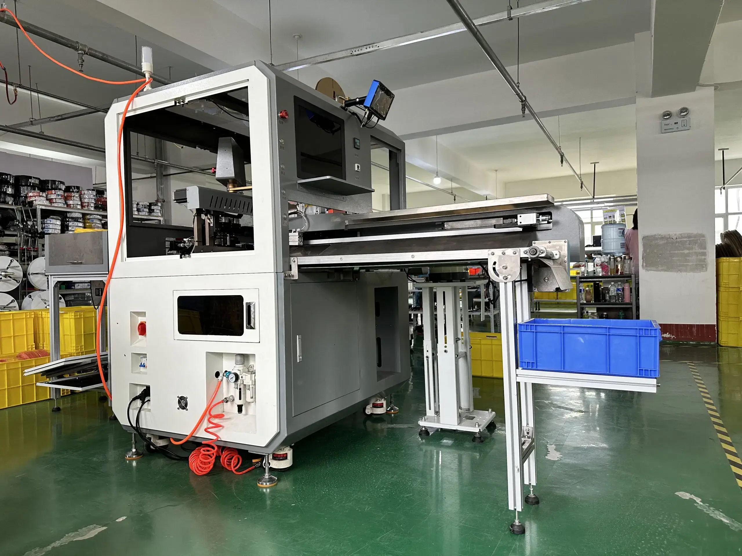
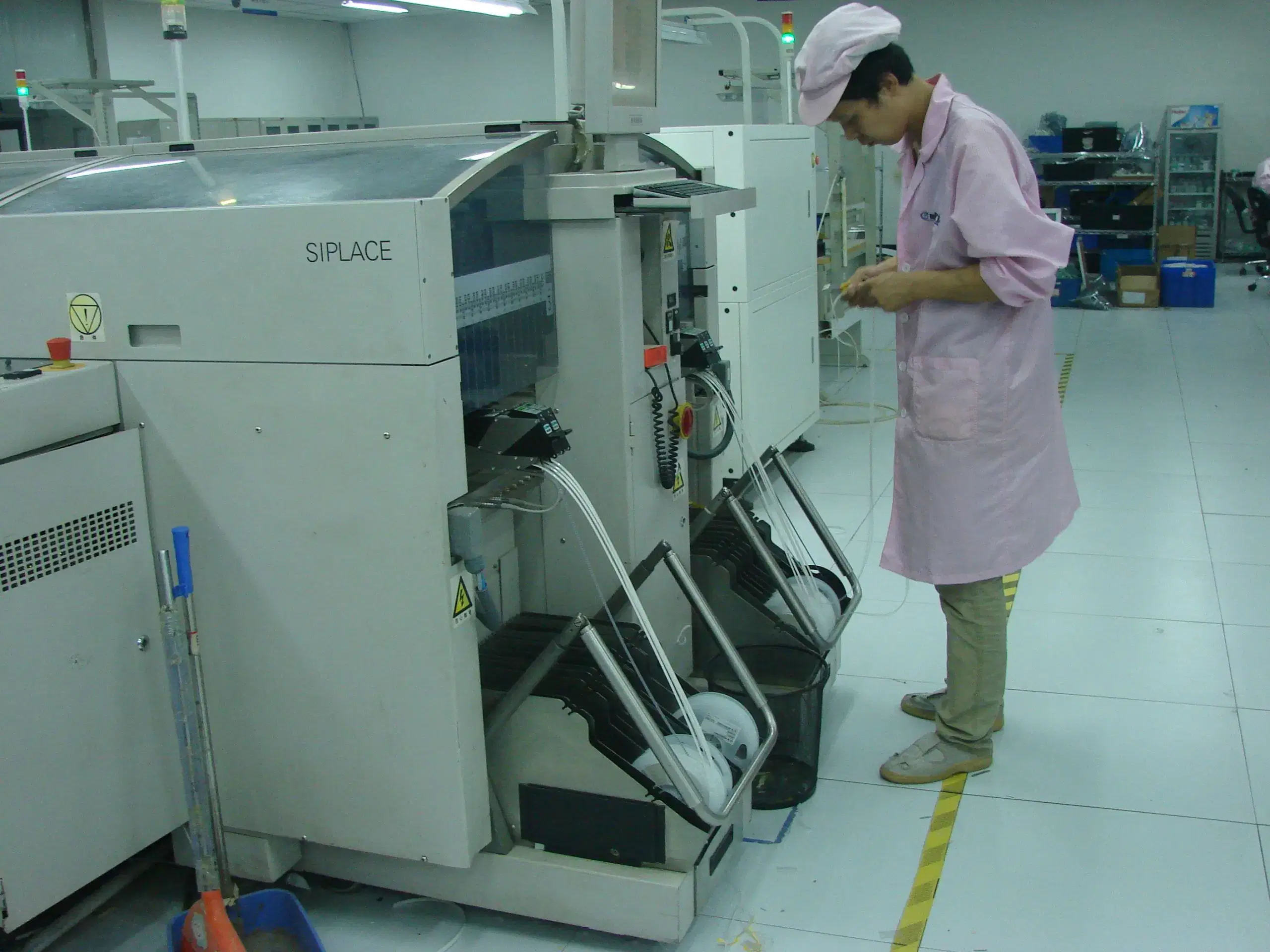
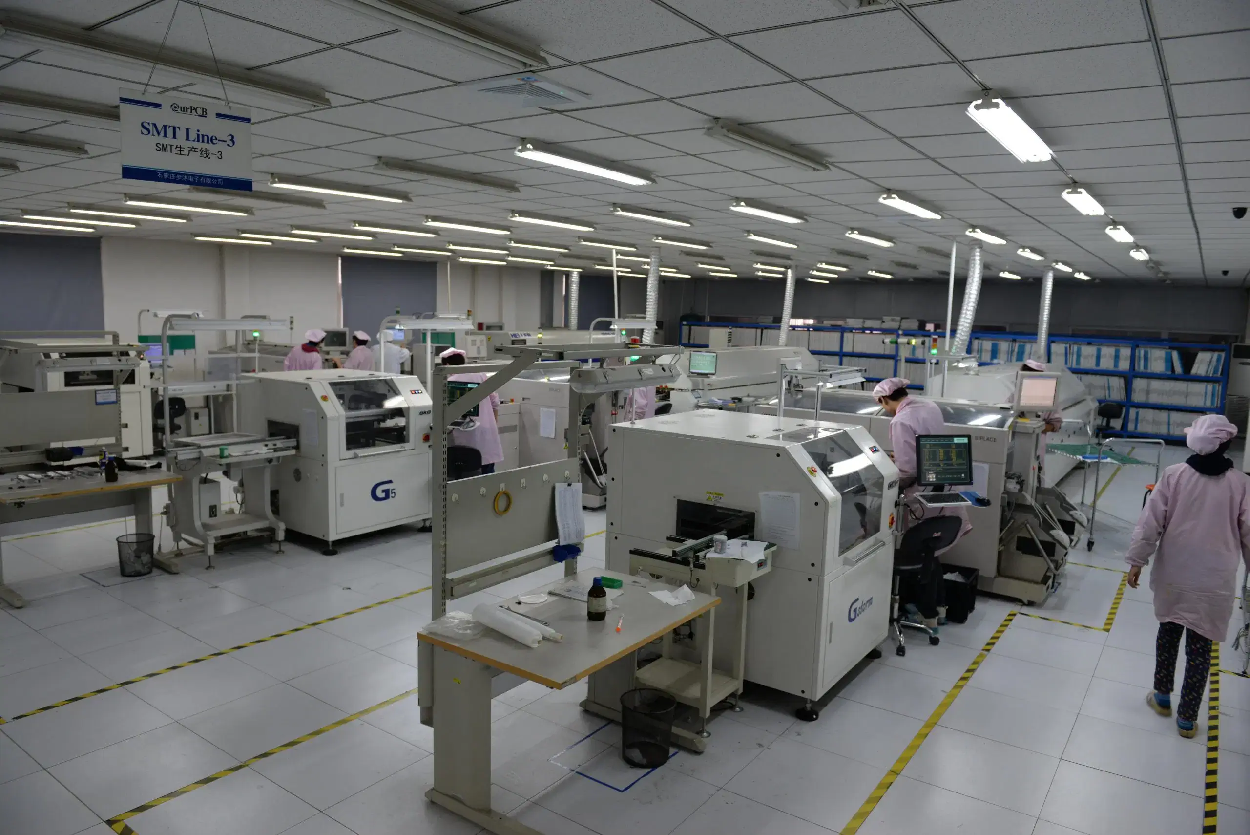
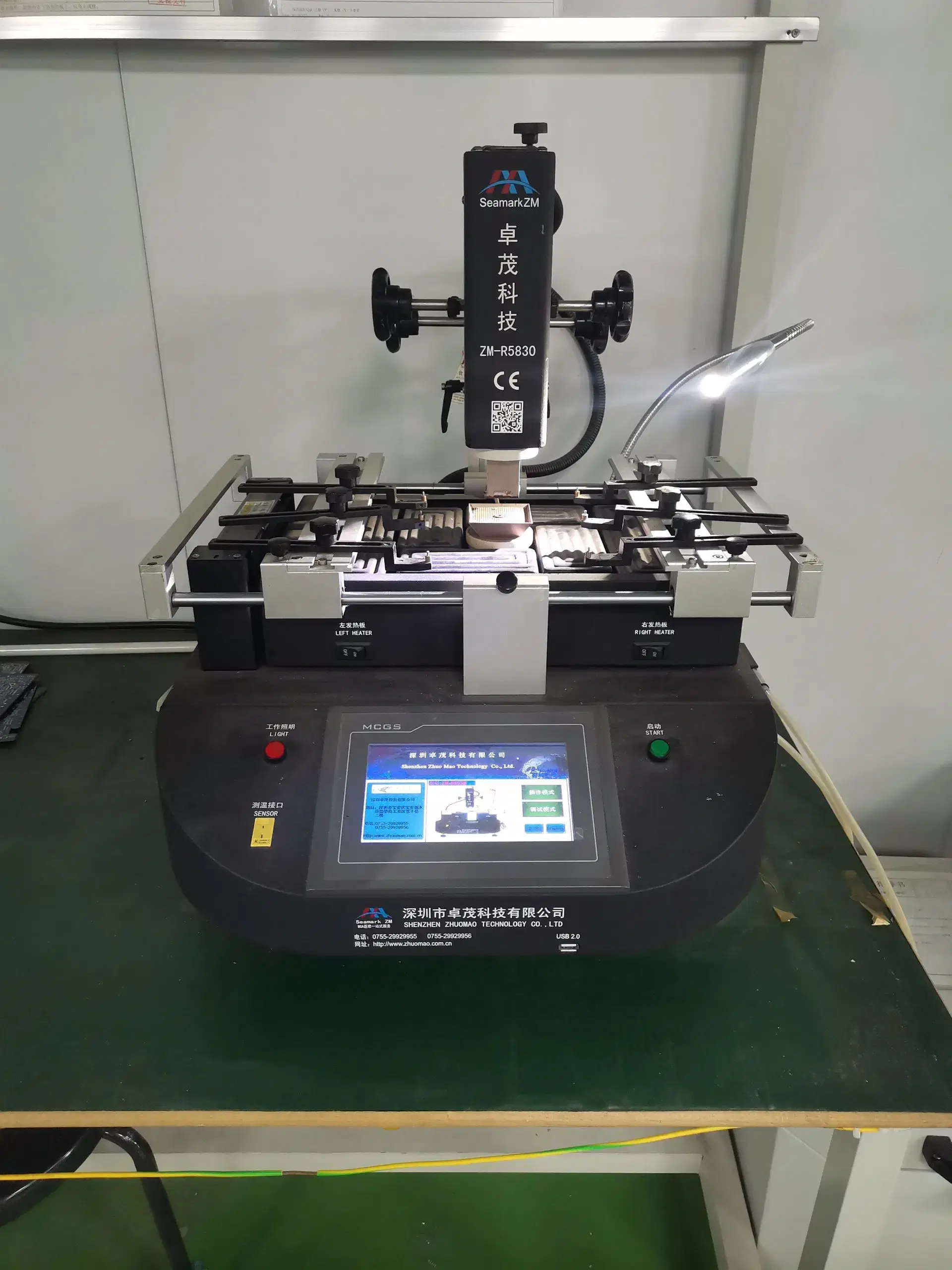
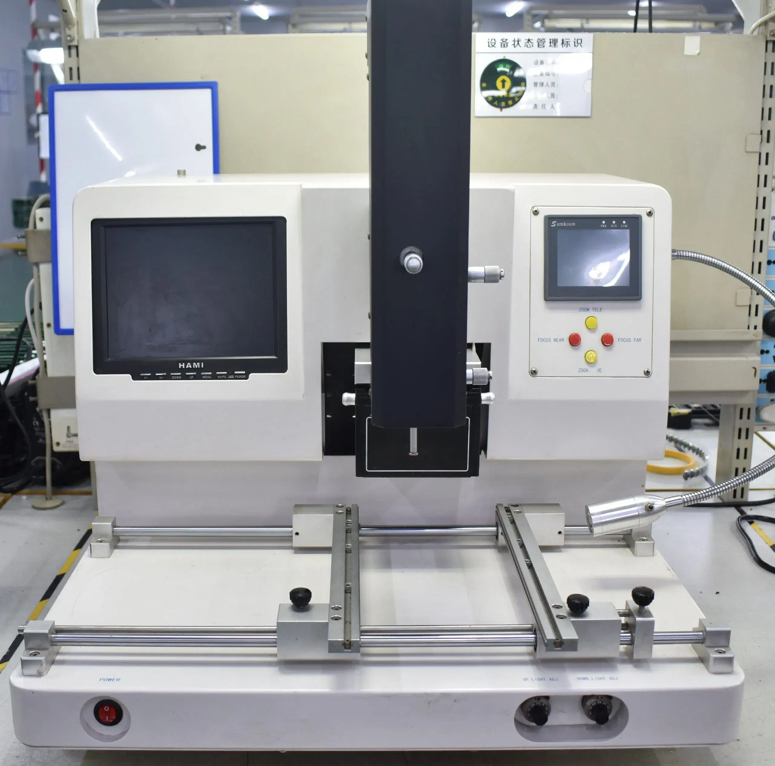
Our PCB Factory Gallery

Frequently Asked Questions
Standard PCB assembly typically focuses on the soldering aspects of the circuit board. However, IoT PCB assembly incorporates standard soldering requirements as well as additional items such as antenna clearance, wireless layout, low-power states, sensors, unique IDs, and custom FCT for configuration.
These elements of IoT PCB assembly connect the assembled product to RF performance, battery operation, cloud integration, and traceability of the final assembled product.
Sleep current can have a significant impact on the operation of a battery-operated device. It is important to test battery-powered devices for sleep current under the conditions outlined in the sleep-current section above.
While PCBA assembly and RF testing may provide supporting data, they do not constitute compliance for the finished product. The final product must comply with the evaluated radio, antenna, enclosure, cables, power supply, and firmware. To prove compliance, a qualified lab must conduct the necessary testing and evaluations.
The failure of IoT products can be attributed to a combination of issues, including changes in configuration, antenna detuning, contamination or leakage, inadequate environmental protection, poor support of connectors, component substitutions, firmware or identity issues, and test conditions that do not reflect true operational states.
By keeping records of IoT production, you may reduce the likelihood of these possible failure modes occurring. You will have an easier time identifying and investigating the root cause of failures.