Upload BOM & Gerber
-
Mobile: +86 13312967631
-
Email: sales@sugaintl.com

High Frequency 5G Telecom PCB Assembly
Telecom PCB Manufacturing Services For 5G RF, HDI, And mmWave Boards
Our telecom PCB manufacturing services focus on 5G boards where RF laminate choice, HDI structure, impedance control, and traceable RF testing decide whether the build can pass production.
1-40 Layers / 0.2-5.0mm Board Thickness
4mil Laser Drilling / 2.7mil Trace-Space
±5Ω / ±10% Impedance Control
VNA, TDR, AOI, X-ray / AXI, E-Test
What Is a 5G PCB, and What Changes at the Board Level?
A 5G PCB is a PCB designed for 5G bandwidth, frequency, signal loss, antenna, and testing requirements. It is defined as a 5G PCB when the parameters of the RF path, laminate selection for the PCB, antenna placement, stack-up, thermal path, and testing requirements align with the frequency and bandwidth required for the hardware.
The transition to a 5G PCB begins before the routing of the PCB. Designing a PCB for channels from 100 MHz to 400 MHz, FR1 or FR2 operating bands with a target data rate of 20 Gbps, or latency of 1 ms influences the design choices made on how to safely protect the traces on the PCB. The elements of PCB construction, such as material loss, copper roughness, via stubs, antenna clearance, and variations in the assembly, will begin to impact the design choices.
| Feature | 4G technology | 5G technology | Board-level implication | Follow-up area |
|---|---|---|---|---|
| Channel bandwidth | 20 MHz | 100 MHz to 400 MHz | Wider bandwidth raises loss-budget pressure and makes laminate choice more important. | Material selection |
| Frequency range | 600 MHz to 5.925 GHz | FR1 / sub-6 GHz plus FR2 mmWave examples such as 24.25-43.5 GHz; 77-81 GHz belongs to specialized radar cases | mmWave frequency makes antenna layout, return paths, copper surface loss, and testing more sensitive. | Antenna layout, loss control, use cases |
| Maximum signal rate | 1 Gbps | 20 Gbps | Faster signaling increases the cost of impedance mismatch, stubs, and rough copper paths. | Signal loss and HDI |
| Latency | 10 ms | 1 ms or less | Low-latency hardware pushes tighter testing across RF routing, assembly, and test. | Assembly and test |

Why 5G Board Constraints Start Before Layout
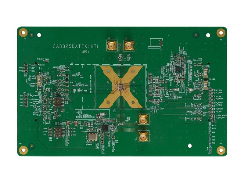
The primary function of 5G Base Station PCBs is not determined by layout. Instead, your choice of laminate family, placement of antennas on your PCB, depth of stack-up, and RF test path are already limited by the target band and bandwidth.
If the PCB does not exceed the high-frequency RF stresses, the process typically used for FR-4-based applications will likely be able to support these types of additional circuitry as it pertains to 5G Base Station applications. However, once the design progresses into low loss RF paths or mmWave usage, the PCB material type, material properties, and antenna designs will begin to dictate how you route your PCB.
Bandwidth Changes That Reshape PCB Decisions
Where there is a change in bandwidth, the number of mistakes that can occur at the lowest frequencies is now magnified significantly with subsequent frequency increases. For example, trace line discontinuities, return path quality issues, or copper roughness may or may not have had a significant effect on the overall RF performance of the control PCB at lower frequencies. However, the same PCB carrying 5G signals and going up to the highest operating frequency will now have quantifiable RF loss due to these very same types of things that occurred at lower operating frequencies.
From Design Requirement To Manufacturing Risk
If you look at a 5G Base Station as a design requirement, it then becomes a manufacturing issue. Can the laminate that you selected be manufactured within an acceptable level of consistency? Does the High-Density Interconnect (HDI) structure, if applicable, support the design density of the module? After soldering, will any changes made during assembly and testing be caught and corrected prior to being declared good? Each of these questions corresponds to a subsequent section of this paper.
Material Choices Behind mmWave PCB Loss
FR-4 with a Dissipation Factor (Df) of between 0.015-0.020; RO4350B with Df of about 0.0037; RO3003 with Df ~0.0010; and Polytetrafluoroethylene (PTFE) with Df of ~0.0009 do not belong in the same loss category for mmWave PCBs. Therefore, the material selection process for mmWave applications will be based on Df, Dk stability, frequency range, and processing history/characterization. The cost of a material selection for mmWave applications comes after you have adequately made a determination on the loss path.
When selecting mmWave materials, one should consider the conditions under which the RF path begins to not allow for any further losses due to moisture, poor copper bonding, or instability of the impedance of the RF path and not necessarily use a name that sounds "better" because it is mmWave.
| Material | Dk / design note | Df @ 10 GHz / loss note | Frequency fit | Processing level | Best-fit 5G / RF hardware | Decision use |
|---|---|---|---|---|---|---|
| FR-4 Standard | 4.2-4.5 | 0.015-0.020 | Cost-sensitive low-frequency or sub-3 GHz control sections | Standard | Control boards, support circuits, non-mmWave paths | Fit for non-mmWave-sensitive RF link budgets and support circuitry. |
| Rogers RO4350B | 3.48 +/- 0.05; Tg >280°C | 0.0037 | Commonly used from sub-6 GHz through higher microwave design contexts | FR-4-compatible processing | Sub-6 GHz RF, moderate RF links, cost-balanced 5G boards | Balances RF loss, cost, and standard fabrication behavior. |
| Rogers RO3003 | 3.00 | 0.0010 | 24-40 GHz mmWave RF designs and higher-frequency microwave links | Specialized RF laminate | mmWave links, base station RF paths, longer RF traces | Fits low-insertion-loss paths; radar/test-equipment use cases at 77-81 GHz stay under specialized mmWave cases. |
| Rogers RO3006 | 6.50 | 0.0020 | Compact RF designs where higher Dk helps reduce circuit size | Specialized RF laminate | size-constrained RF modules, filters, couplers, compact microwave circuits | Fits compact RF layouts where higher Dk supports size reduction. |
| RT/duroid 5880 / PTFE family | 2.20 | 0.0009; low moisture absorption around 0.02% | Demanding low-loss microwave / mmWave paths, including DC to 110 GHz use contexts | Specialized PTFE processing | phased arrays, satellite links, RF test equipment, long low-loss lines | Fits the hardest low-loss paths where PTFE processing is acceptable. |
| PTFE low-loss materials | around 2.1-2.3 depending on grade | 0.0009-0.0012; moisture can be below 0.01% for some PTFE systems | 40 GHz+ and very low-loss paths | Specialized drilling / bonding preparation; some PTFE systems carry a 4-8x FR-4 cost boundary | low-loss mmWave and microwave paths | Fits designs where loss dominates the decision and PTFE bonding is controlled. |
| LCP | 2.9-3.2 | 0.002-0.004 | Flexible 5G / RF bands and compact modules | Specialized; limited fabricator availability may affect timing | flexible antenna paths, compact module routing, flex/rigid-flex RF sections | Fits flexible RF paths where bendable geometry and low loss must be balanced. |
| RO4730G3 | about 3.0 | around 0.0029 | antenna / RF laminate option where low loss and stable RF behavior are needed | RF laminate | antenna boards, RF feed sections, cost-balanced RF layouts | Adds a stable RF laminate option for antenna and feed sections. |
| TC350 Plus | Dk 3.5; TCDk is relevant | Df 0.0017; thermal conductivity 1.24 W/m-K | 5G power amplifier and thermal-sensitive RF sections | Thermal-focused RF laminate | power amplifier circuits, RF power areas, antenna feed sections | Fits RF power areas where heat flow matters as much as low loss. |
Which Frequency Band Sets the Laminate Choice?
A sub-6 GHz control or support section will be able to accommodate a different material than the 24-40 GHz RF path or specialized mmWave test path. When working with the new 5G technology, separate out the telecom band and specialized mmWave cases. Multiple types of RF laminates such as RO3003, PTFE, LCP, and other RF laminates may be used in the same project; however, most of the time they will be performing different functions for the RF paths.
Dk and Df Before Loss Budgeting
Df is the measure of how much energy a material loses, whereas Dk affects impedance, trace width, and field behavior. Therefore, prior to creating a loss budget, it is essential to understand how to read both of those properties.
For high-frequency laminate, Df 0.004 or less is typically a target threshold; however, it is not the sole determining factor in the decision-making process. Although lower Df materials will yield less overall energy loss, these materials can present challenges regarding processing, moisture, bonding, and thermal performance.
Rogers Materials for Balanced RF Loss
Rogers RO4350B is a good example of a material that sits in between standard FR-4 and more specialized PTFE-class materials. Even though Rogers RO4350B provides lower loss than FR-4, it still stays closer to standard fabrication behavior than PTFE-class materials.
RO3003 indicates a transition to lower Df and more demanding microwave paths. When you have a situation where insertion loss is more critical than material cost, using RO3003 becomes advantageous; however, RO3003 also requires careful processing to control dimensionality and physical properties during fabrication.
When Does FR4 Stop Working?
FR-4 should not be your go-to option when it comes to RF paths that are sensitive to RF loss. While Df values in the range of 0.015-0.020 may be acceptable for control or low-frequency support boards, they will not provide a mmWave answer.
FR-4 should not be eliminated too soon from the project. Any section of your project that has acceptable RF budgets should incorporate FR-4; conversely, any sections that require low-loss laminates should reserve low-loss materials for those specific applications.
PTFE and LCP at the Edge of mmWave
PTFE and LCP solve different problems in regard to mmWave applications. PTFE materials fit very low-loss microwave and mmWave frequencies. LCP materials assist in producing compact or flexible RF structures that require both low loss and a bendable material.
If any aspect of the process, such as copper bonding, drilling, laminate handling, or material availability, is incompatible with your design, then you will be unable to benefit from the advantages that PTFE and LCP provide.
5G Antenna PCB Layout and Beamforming
Mistakes in the placement of 5G antenna components on your PCB can affect the performance of your beam coverage before you ever complete the design of your PCB. In designing a 5G antenna PCB, the placement of antennas, the behavior of the ground plane, the relative lengths of the traces, isolation, and the types and patterns of antennas will dictate the RF performance of the board before dense routing begins.
| Layout node | What it changes | Engineering use |
|---|---|---|
| Antenna location | Placement belongs in the design phase, not after routing. | Start antenna clearance, housing, and RF path decisions before the board is crowded. |
| Ground plane and trace length | Ground plane support and shorter trace length reduce noise and improve efficiency. | Keep the antenna close to the wireless module where the mechanical design allows it. |
| Isolation between antennas | Multiple antennas need distance and orientation control. | Prevent antennas from coupling into each other in MIMO or beamforming layouts. |
| Beam coverage | PCB geometry can distort coverage when spacing or orientation is wrong. | Treat coverage loss as a board-level failure mode, not only an antenna-spec issue. |
| Antenna type choice | Patch, monopole, and dipole choices depend on radiation pattern, beamwidth, frequency band, size, and gain. | Pick the antenna structure before freezing the board outline and RF keep-outs. |
Antenna Placement Before RF Routing
The information gives general instructions about layouts for PCBs that are being designed for use with RF transmissions. The layout must take into consideration the RF transmission techniques, such as MIMO and beamforming, that will be used, as well as the housing, RF path, distance between antennas, and how coupling of multiple antennas can distort RF coverage or cause interference between the RF signals.
The various types of antennas available for use in an RF application, including patch, monopole, and dipole, should be chosen before the board has been defined, and their placement on the board should occur near the front of the RF layout process.
Once an antenna is chosen, the layout can start to build the board to accommodate those choices. The density and size of the enclosure need to be sized to fit the antenna chosen, and the ground-plane area must have enough copper to adequately support the radiation pattern created by the antennas being used.
The ground-plane area must also account for the length of the traces as well as where those traces will attach to the wireless module. Before designing a 5G product, the designer must determine how the size, type, and locations of the antennas will impact the design.
Beamforming Pressure on PCB Geometry
The design must take into account how the layout will be affected by the beamforming methods used. For instance, a 4×4 antenna array installed in a single area of space does not mean it will have four effective transmission paths when the spacing is too close. Each of those antennas is affected by the proximity of the copper, ground structure, housing, and other nearby antennas.
Where Small Antenna Errors Distort Coverage
The layout must take into consideration how coupling of multiple antennas can distort RF coverage or cause interference between the RF signals.
Miniaturized Antenna Boards
Compact, small enclosures are beginning to limit the amount of design space available within the PCB for the RF module. With limited RF coverage, antenna clearance is restricted, which forces routing into the densest part of the enclosure, even with routing stress being placed on the PCB.
Additionally, due to the limitations of a 5G device's size, compact design constraints can create smaller enclosures, but they will also create more extensive routing complexity. Therefore, proper layouts will have to be completed early in the design process to ensure there is enough time to design for the appropriate routing of RF traces and avoid accidental connections.
Antenna Type Choices: Patch, Monopole, and Dipole
The various types of antennas available for use in an RF application, including patch, monopole, and dipole, should be chosen before the board has been defined.
Where Signal Loss Accumulates in 5G PCBs
Signal loss is not limited to the RF module where it gets transmitted, as previously mentioned. It occurs along the entire length of the RF path, starting with the signal source (IC) and continuing through the board, the antenna or multiple antennas, and back. To properly calculate the amount of signal loss, the designer will need to use manufacturers' Df, copper roughness characteristics, and other factors that could impede the signal between the source and the load.
Signal loss does not just occur in one location within the RF path. Signal loss accumulates through the entire length of the RF path. The input condition is determined by the dissipation factor (Df) of the material used. Copper roughness contributes to conductor losses through the copper traces. If the return path of an RF circuit is interrupted by a connection or lack of connection between the ground plane and PCB substrate, the RF energy will reflect back toward its source. Additionally, the placement of via stubs, if used, in a PCB will create energy reflections, as will densely routed traces, causing EMI or crosstalk.
| Loss type | Mechanism | Design response | PCB design checkpoint | Verification link |
|---|---|---|---|---|
| Dielectric loss | Loss is driven by material Df and Dk behavior. | Use low-Df materials where the loss budget needs them. | Confirm the material stack-up against the RF path. | Confirm material stack-up and loss budget. |
| Conductor loss | Skin effect and copper roughness increase insertion loss. | Use smooth copper and controlled RF layer planning. | Check copper roughness, copper weight, and RF trace layer choice. | Compare insertion loss through S-parameters. |
| Return-path disruption | Broken ground reference creates impedance discontinuity. | Route high-speed RF over a solid ground plane. | Check ground plane continuity under RF paths. | Use VNA / S-parameter testing after assembly. |
| Via stub loss | Stub length creates reflections and impedance mismatch. | Minimize stub lengths. | Decide whether backdrill or blind-via strategy is needed. | Connect to HDI capability. |
| EMI / crosstalk | Dense analog and digital frequencies interfere. | Separate traces and use multilayer routing. | Check isolation, shielding, and route spacing around dense RF paths. | Connect to EMI testing. |
Conductor Loss and Copper Roughness
At high frequencies, the skin effect causes the current to crowd near the surface of the conductor. The rough surface of the copper gives the signal greater surface area to travel across and increases the insertion loss of the RF path.
The copper weight of the conductor is still important for current distribution and thermal effects, but the fact that the copper weight has to be sufficient does not always translate to providing a high-performance RF path. For high-speed RF layers, the profile of the copper, trace geometry, and impedance characteristics must all align.
How Return Paths Break Signal Integrity
When an RF trace is split by a plane, gap, via hole, or bad transition, you lose continuity on the return path. The result is an impedance mismatch for the signal, and it will be reflected, distorted, or poorly returned by way of that discontinuity. In a good reference plane, this problem can be minimized.
Via Stubs as a Signal-Loss Source
Via stubs form an unused transmission line. Stub reflections may not be significant at low frequencies, but when they are present at higher frequencies, they can return energy into your signal path.
EMI and Crosstalk Around Dense RF Routing
When RF routing is densified, the analog, digital, power, and control paths are closer together, and EMI and crosstalk occur as layout failures rather than compliance concerns.
Thermal Stress in Telecom PCBs
Low Df alone cannot supply a stable thermal path for your telecom PCB. You may design your telecom PCB with a low-loss RF laminate and still have thermal failure if the heat produced by power amplifiers, antenna feeds, dense HDI areas, or the enclosure does not leave the PCB fast enough.
TC350 Plus can help your design by establishing Df 0.0017 and thermal conductivity 1.24 W/m-K at 10 GHz. The first value indicates loss, and the second value tells you how well the heat will be able to flow away from your PCB and into the surrounding environment. Both of these values are factors when designing your PCB.
Heat Paths Through Vias and Copper
Somehow heat must leave the RF power area. The various elements that make up a telecom printed circuit board (PCB) or radio frequency (RF) module need to work together for the best thermal performance. Thermal vias carry heat to the PCB vertically, copper planes distribute it across the board horizontally, and heat sinks or cooling fans are used when the PCB cannot support the heat load on its own.
On the other hand, the thermal path for 5G base stations must be created specifically with the same high level of consideration as the signal path. If the PCB thermal path traps heat near a power amplifier or other high-density copper area, the RF component thermal management may suffer even when the RF component itself meets the specified loss target.
When Thermal Conductivity Matters More Than Df
When referring to thermal performance, it is important to understand the role of thermal conductivity (TC) versus dielectric loss factor (Df). Dielectric loss factors protect the communication signal from being lost while thermal conductivity protects the surrounding hardware from damage. For the design and construction of power amplifiers and antenna feed components, thermal management may ultimately become the most important factor in the design process.
TC350 Plus is more than just a low-loss material. Its thermal conductivity of 1.24 W/m-K alerts engineers to consider how the laminate, vias, metal areas, and enclosures interact to remove heat from the RF power generation zone.
CTE, Humidity, and Field Deployment
When designing telecom PCB systems for operation in the field, consider the unique stresses placed on the boards when exposed to temperatures outside their rated operating range. The thermal cycling processes that take place from temperature changes and moisture exposure may result in CTE mismatch issues that can cause mechanical movement when subjected to extreme temperature fluctuations over time.
The performance of a telecom PCB will ultimately be determined primarily by how it performs after it has been subjected to exposure to different environmental conditions as opposed to how it performs under the controlled testing conditions used during the normal development of a PCB. Moisture exposure, temperature cycling, and the heat generated by an enclosure all have a direct effect on the performance of a telecom PCB during field operation.
Thermal Simulation Before Final Layout
The most effective method of ensuring that the PCB layout will successfully manage heat is to perform thermal simulations prior to finalizing the layout. This allows the engineering design teams to evaluate whether components, vias, copper planes, and heat sink configurations are capable of moving heat away from RF-sensitive areas of the PCB successfully.
HDI PCB for 5G Modules
The number of layers that comprise high-density interconnect (HDI) PCB modules for 5G applications is determined by the spacing and width of the conductor traces, the size and type of components, and the overall shape of the modules.
| Capability | Value | Module use | RF consequence | Manufacturing note |
|---|---|---|---|---|
| Layer count | 1-40 layers | Supports multilayer RF, power, and control routing in compact modules. | More layers can separate RF, power, and ground paths. | Match layer count to stack-up complexity. |
| Board thickness | 0.2-5.0mm | Helps fit compact or mechanically constrained module formats. | Thickness affects impedance stack-up and mechanical reliability. | Match thickness to enclosure and RF stack-up. |
| Laser drilling | 4mil | Supports microvia-style dense interconnect routing. | Reduces routing congestion around fine-pitch RF sections. | Confirm registration, plating, and stack-up discipline. |
| Min spacing / tracing | 2.7mil/2.7mil; 2 mil trace / space | Supports dense 5G module escape routing. | Narrow features raise impedance and yield sensitivity. | Use tighter trace/space only where the module density requires it. |
| HDI / blind and buried / backdrill | Listed as board type capability | Lets modules reduce via stubs and route compact RF paths. | Backdrill or blind vias can reduce reflection risk. | Use when stub reduction or compact routing is needed. |
| mSAP | straighter, more precise traces | Useful when fine traces must keep geometry stable. | Helps avoid trapezoidal trace issues and impedance discontinuity. | Use where geometry stability matters. |
Which HDI Features Help 5G Modules?
When RF routing must be compact, have a narrow pitch escape, or have a short interconnect path, HDI provides help to a module.
The use of blind vias and buried vias will help reduce routing pressure.
The use of backdrill can reduce stub behavior in cases when using a through via would leave too much unused via barrel.
Backdrill and Blind-Via Fabrication Limits
The problems solved by backdrilling and blind vias are different.
Backdrilling is used to remove unused length in vias that can reflect RF energy.
Blind vias and buried vias are used to shorten transitions and create routing space in dense modules.
The use of a 4mil laser drilling capability will be important when using microvia interconnects, but the registration, plating, and stack-up discipline must still be maintained.
Fine Trace Limits and mSAP Options in Dense 5G Hardware
Fine trace and space limits provide benefits for the escape path of compact modules; however, fine trace and space limits also increase the manufacturing sensitivity of a design.
A design that uses a 2.7mil/2.7mil trace / space or 2 mil trace / space will have less margin for process drift.
mSAP allows for straighter and more accurate traces than subtractive processing when geometry stability is important.
Rigid-Flex Options in Telecom Devices
Rigid-flex offers an alternative method to interconnect the antenna, module, and enclosure geometry of a compact telecom device without introducing an awkward board-to-board transition.
Achieving an electrical goal requires consideration of bend radius, copper fatigue, antenna clearance, and assembly handling.
5G Base Station PCB, RF Modules and mmWave Use Cases
Different applications of 5G PCB will present varied problems. A mobile or IoT design, an RF module, a specialized mmWave board, and a base station PCB each represent a different engineering limit.
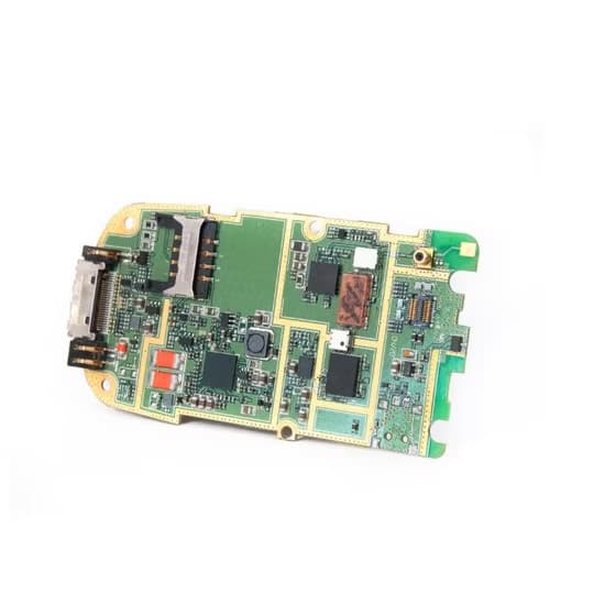
Base Station Architecture Behind 5G PCB Demand
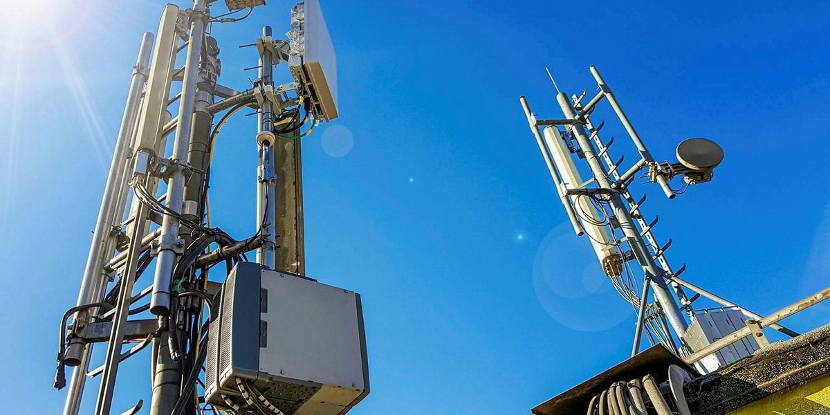
5G base station architecture is demanding a higher density of boards than ever before due to the increased number of antennas and smaller size. Currently, base station and active antenna unit (AAU) hardware must meet two important criteria: the physical size of the board and the thermal density. Manufacturing capability defines the maximum physical size of the infrastructure-scale RF boards as approximately the 1100mm x 500mm panel size referenced in the manufacturing capabilities section. The large physical size of the RF board increases the risk of misalignment and warpage prior to any RF performance testing being performed. Also, the combined multiple antenna array RF routes create a high concentration of heat in the same location where there is the greatest concentrated routing of RF — the same laminate-to-routing thermal considerations previously described that are magnified because of the increase in RF routes at once. Therefore, passing thermal checks at small board size is not an acceptable predictor of success for a truly large-scale infrastructure base station PCB.
RF Module PCB in 5G Hardware
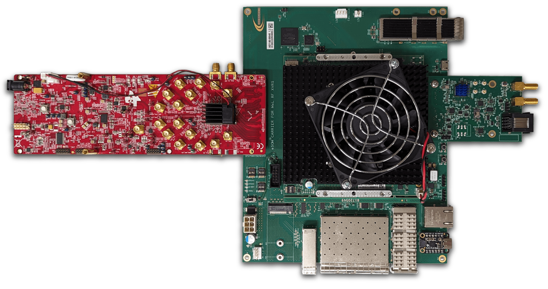
Base station RF module PCBs are where three disparate design decisions must be made on one layout: laminate material selection, compact high-density internal routing from module capability, and the assembled final PCB testing outcome based on testing results. Thus, a base station RF module's failure may be due to these decisions being optimized separately, rather than due to isolated routing or laminate material failure. The same three decisions need to be optimized together on the same layout prior to PCB manufacture.
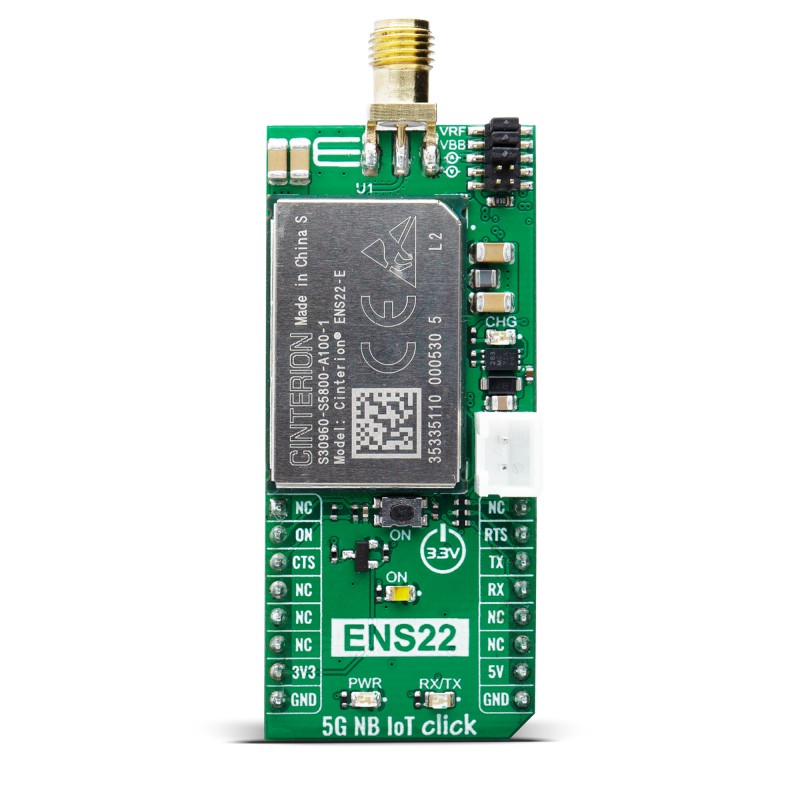
Mobile and IoT 5G PCB Designs
Mobile, wearable, and IoT devices have made routing density the primary limiting constraint for PCBs. Accordingly, antenna clearance is reduced, module routing is becoming denser, and designs will either include rigid-flex or more compact HDI designs. This trend will require more extensive antenna and stack-up planning given that a small enclosure can completely obscure a substantial RF design compromise — the fine trace and mSAP options described earlier primarily exist to resolve this design space issue, not as general manufacturing upgrades.
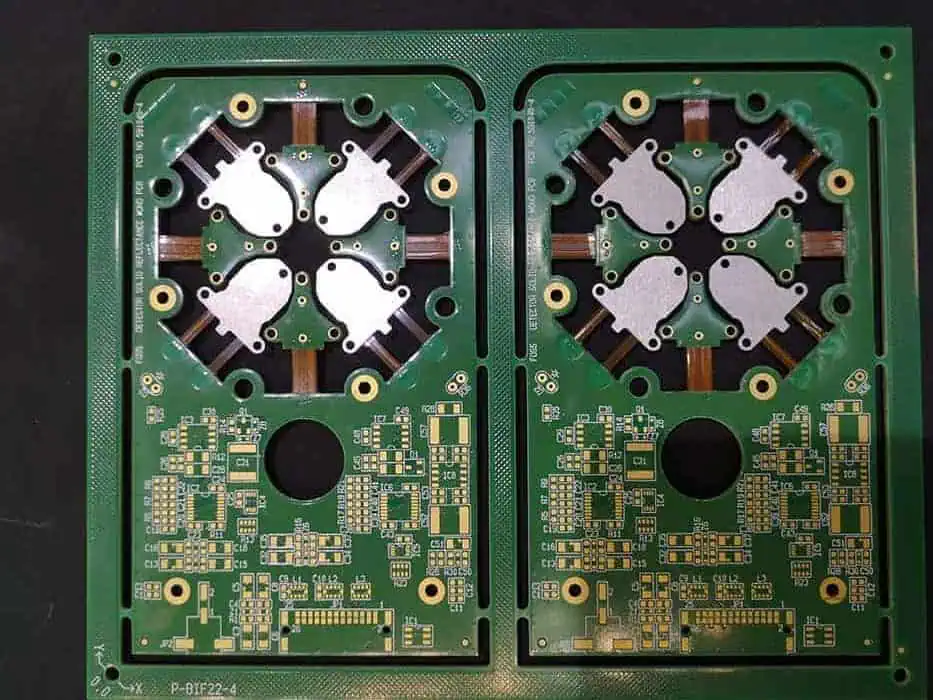
Specialized mmWave PCB Cases: Radar, Satellite and Test Equipment
The case for specialized mmWave PCB applications demonstrates the shifting frequency pressures. Automotive radar in the 77-81 GHz band, satellites communicating through 26.5-40 GHz Ka-band and 12-18 GHz Ku-band, and RF test equipment approaching the 110 GHz range all necessitate more stringent material specifications than previously described. Automotive radar and RF test equipment are often pushing toward PTFE-family materials, while Rogers RO3003-class materials may still be appropriate for the lower frequency end of this range. The frequency ultimately dictates what laminate family can be used before the cost and delivery issues are evaluated.
Telecom PCB Assembly and Test
Finally, the connection between PCB assembly inspection methodology and catching specific failure modes is essential in the telecommunications industry. Each of the methods employed, VNA / S-parameters, TDR, AOI, X-ray / AXI, E-Test, microsectioning, thermal cycling, EMI testing, and traceability, addresses distinct failure risks associated with a PCB assembly and will help determine how to proactively deal with and mitigate potential process issues.
| Test method | What it catches | Linked risk | Record role |
|---|---|---|---|
| VNA / S-parameters | RF path loss, return loss, and impedance behavior | Signal integrity failure after assembly | RF measurement record |
| TDR / impedance coupon | Controlled impedance deviation and stack-up mismatch | RF path mismatch, reflection, and inconsistent lot behavior | Impedance verification complement |
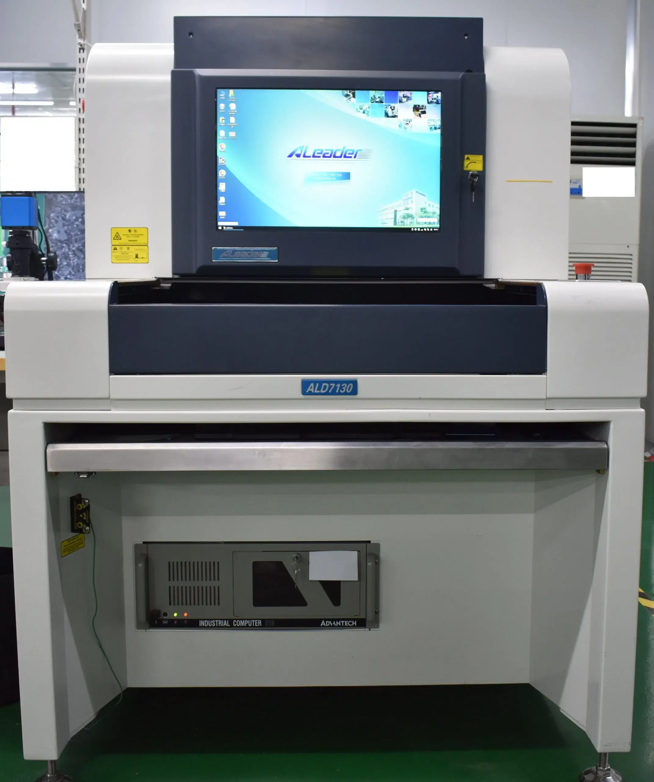
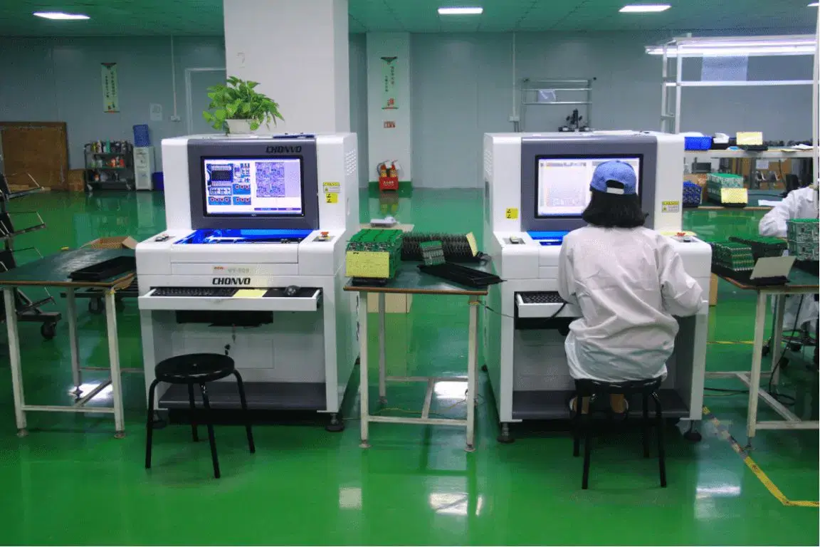
| AOI | Placement, solder, and visible board defects | Assembly defects before later test stages | Visible assembly inspection |
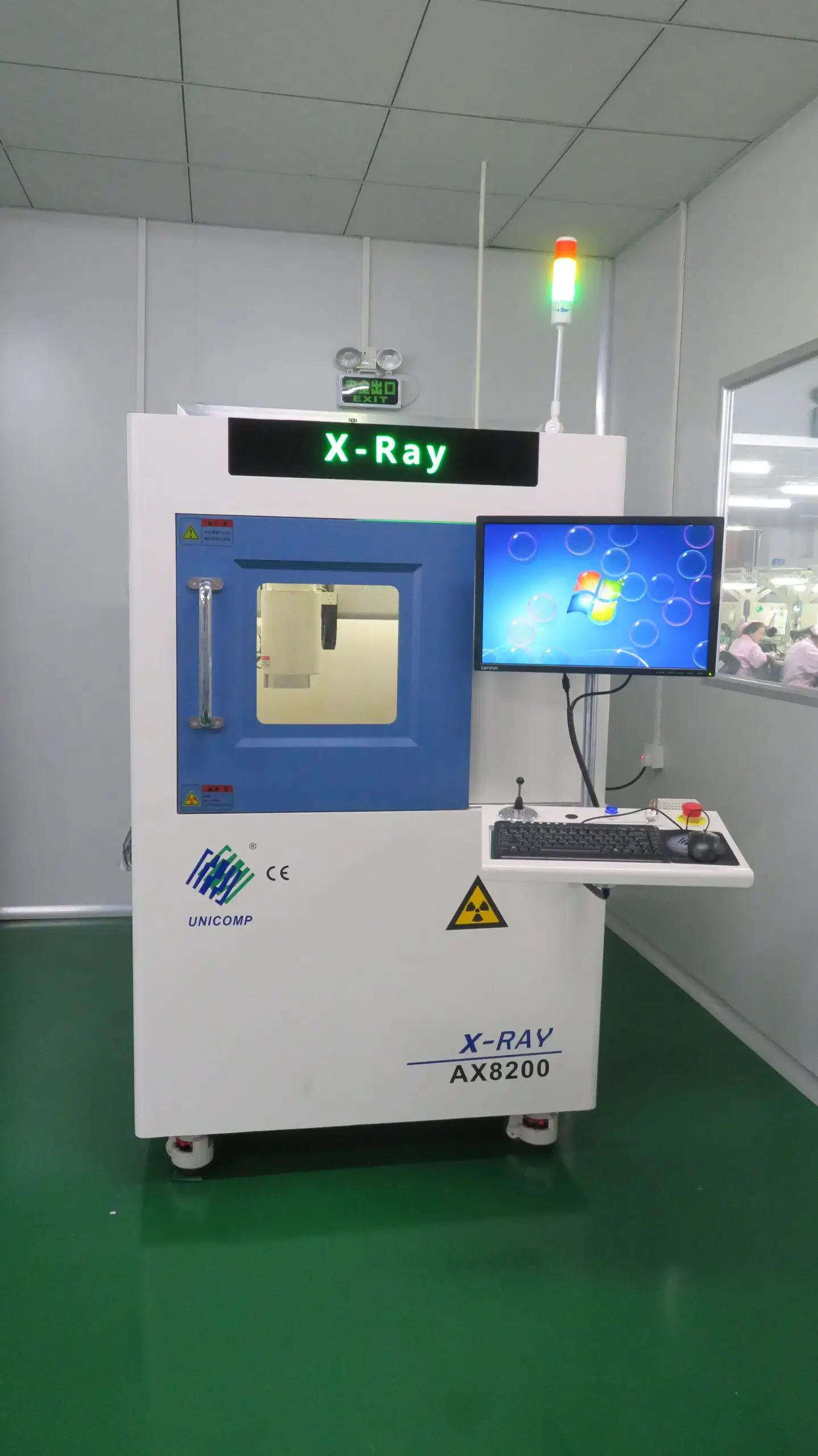
| X-ray / AXI | Hidden solder joints, BGA voids, and inaccessible assembly defects | Fine-pitch BGA and module assembly risk | Hidden-joint inspection |
| E-Test | Electrical continuity and circuit-level faults | Open / short / electrical mismatch | Electrical continuity record |
| Microsection / cross-section | Plating wall, via quality, microvia structure, backdrill quality, and laminate construction | HDI reliability, PTH wall risk, microvia fatigue, and fabrication data gap | Destructive structural record |
| Thermal cycling | Material stability under temperature change | Thermal stress and CTE-related reliability | Stress record |
| EMI testing | Electromagnetic interference behavior | Dense RF routing and shielding risk | Interference record |
| Traceability | Records across telecom assembly | Lot accountability and compliance support | Process record |
One single test does not typically resolve all questions. For instance, you may need to use both microsection and X-ray / AXI to inspect soldering problems because X-ray will show hidden defects that are not visible with microsection, and microsection will show how well your vias and plating are constructed. In any RF application, to determine RF impedance questions, you may need both a Time Domain Reflectometer (TDR) and Vector Network Analyzer (VNA) / S-parameters testing. The TDR helps you locate discontinuities in the trace, while the S-parameters provide RF behavior or performance.
Why High-Frequency Telecom PCBs Need Precision Assembly
Due to the high frequency of the RF signals, the precision of the assembly of the PCB becomes of increased importance. A very small deviation from placement, soldering, or routing can cause an RF failure, whereas the same PCB manufactured at low frequencies could withstand this drift without issue. Conversely, a dense RF module will have less tolerance for even minor deviations.
RF Testing With S-Parameters
S-parameters connect the assembled board back to its RF behavior. By using S-parameters, you can measure insertion loss, return loss, and how your signals will behave throughout the entire operational frequency range.
AOI and E-Test Before RF Testing
Before proceeding to RF tests, both AOI (Automated Optical Inspection) and E-Tests (Electrical Tests) have a role to play. AOI reveals the visible defects in the assembly, such as incorrect placement of components, incorrect soldering, and board defects. E-Tests reveal issues related to open and short circuits as well as electrical faults at the circuit level.
Thermal Cycling and EMI Testing
Thermal cycling evaluates the effect that temperature variations would have on the performance of the board. Thermal cycling is also related to thermal expansion (CTE), movement of the dielectric materials, solder joint reliability, and thermal paths in the PCB design.
EMI testing determines how interference occurs due to the routing and shielding options utilized for closely placed RF, digital, and power traces.
Traceability in Telecom PCB Assembly
In many cases, it is even more important to have traceability for RF PCBs than for general PCBs. Most RF failures are either intermittent in nature or influenced by the environment. If an RF PCB has passed the S-parameter test at some point in time but has drifted out of specification after deployment into service, the only way to trace that failure back to the cause is by using traceability.
RF Microwave PCB Manufacturing
RF microwave PCB manufacturing takes capability specifications to yield and RF performance. Impedance tolerance must be +/-5ohm below 50ohm or +/-10% at 50ohm and above when manufacturing RF microwave PCBs. Additional capabilities required for reliable manufacturing of RF microwave PCBs are 10 OZ copper, 25um PTH wall, 3mil annular ring, hybrid RF stack-ups, PTFE treatment if applicable, LCP availability, and surface finish choices.
| Capability | Value | RF consequence | Process boundary |
|---|---|---|---|
| Layer count / spacing / laser drilling | 1-40 layers; 4mil laser drilling; 2.7mil/2.7mil and 2 mil trace / space options | These limits raise yield sensitivity and impedance-control difficulty once RF tolerance is tight. | More layers and tighter spacing add stack-up, registration, lamination, and impedance-control complexity. |
| Board thickness | 0.2-5.0mm | Affects impedance stack-up, stiffness, module fit, and enclosure behavior. | Thin or thick boards need different process checks. |
| Copper thickness | Max. 10 OZ | Supports high-current or thermal paths but can affect RF geometry. | Heavy copper is not automatically suitable for fine RF lines. |
| PTH wall | 25um | Supports hole reliability and plating quality for multilayer RF boards. | Check with microsection / cross-section where reliability matters. |
| Maximum board size | 1100*500mm | Supports large RF panels, backplanes, or infrastructure boards. | Large boards raise registration, warpage, and handling risk. |
| Annular ring | 3mil | Affects via capture, drilling tolerance, and dense interconnect reliability. | Tight annular ring increases registration sensitivity. |
| Impedance control | +/-5ohm(<50ohm), +/-10%(>=50ohm) | Helps keep RF transmission paths within acceptable tolerance. | Must align with stack-up, trace geometry, copper profile, and material choice. |
| Hybrid RF stack-up | Rogers / Taconic / Arlon / Nelco laminate with FR-4 | Balances RF layers with cost or mechanical layers. | Hybrid lamination can change registration, resin flow, and process planning. |
| PTFE processing | sodium etching or plasma treatment for copper bonding | Low-loss PTFE needs special bonding preparation. | Confirm PTFE handling, drilling, and lamination capability. |
| LCP processing | limited fabricator availability and possible 4-6 weeks lead time | Flexible low-loss paths can affect project timing. | Availability and lead time become manufacturing constraints. |
| Surface treatment | ENIG / ENEPIG / immersion silver and others | Surface finish can affect assembly, contact, wire bonding, corrosion resistance, and RF interface needs. | Select based on assembly interface and RF hardware use, not list length. |
| Yield-cost tradeoff | Driven by tight spacing, fine annular ring control, hybrid stack-ups, and special laminate handling | Tighter spacing, finer annular ring, and hybrid stack-ups raise yield sensitivity, which feeds into cost. | Tighter tolerances increase scrap risk and inspection burden. |
RF Microwave PCB Fabrication Limits
All of the factors considered may appear suitable alone, but collectively they may still allow for a failure. For example, even if a PCB satisfies both the thickness requirement and the copper-weight requirement, if the PCB does not meet the overall impedance requirement due to the combined dielectric thickness, copper configuration, trace geometry, etc., it would not meet the impedance target without reference to the total stack-up. The listings on the datasheet that provide impedance-control numbers are only applicable if those numbers have been confirmed on the final stack-up configuration, and not treated as individual capability numbers.
Hybrid RF Stack-Ups
Combining low-loss RF laminates with more traditional laminates provides a means to minimize cost, as well as support stiffness and mechanical structure, while enabling critical RF routing to be maintained on the low-loss RF laminate.
The hybrid lamination process has the potential for changing the registration, resin flow characteristics, drill performance, and impedance control. Therefore, the configuration needs to be finalized before production.
Processing Limits for Rogers, PTFE & LCP Laminates
While RO4350B can be processed similarly to FR-4, PTFE requires special surface preparation, i.e., sodium etching or plasma treatment, and LCP typically has limited manufacturing availability and can have a lead-time boundary of 4-6 weeks.
What Manufacturing Constraints Affect RF Yield?
The design characteristics related to geometry, laminate handling, impedance control, and inspection impact the overall RF yield. Smaller traces may provide better routing space, but they also create a smaller margin in day-to-day processing. Smaller annular rings can increase PCB density, but they will also cause increased registration sensitivity.
How to Choose an RF PCB Manufacturer
Lack of RF/microwave capability, laminate-processing data, DFM support, assembly inspection, RF test data, and relevant compliance records for the desired manufacturer can increase the risk of redesign, yield loss, inconsistent RF measurement, or time constraints when your order reaches production.
| Review category | What to check | Why it matters |
|---|---|---|
| RF microwave manufacturing capability | RF / microwave PCB manufacturing positioning, layer/thickness/copper/impedance capability | The manufacturer is not only a generic PCB shop. |
| Fine-feature fabrication | 2.7mil/2.7mil, 4mil laser drilling, 2 mil trace / space, annular ring control | Dense RF module paths can be manufactured. |
| RF laminate process data | Rogers / PTFE / LCP / hybrid stack-up handling records | Special laminates need proven process handling. |
| DFM / DFA support | DFA & DFM checks before RF production | The manufacturer can catch manufacturability issues before production. |
| Assembly and inspection records | AOI, E-Test, X-ray / AXI, microsection records where needed | Assembly risk is checked before RF-specific testing. |
| RF test data | VNA / S-parameters, TDR / impedance coupon, EMI testing, thermal cycling | RF performance and stress behavior are checked after fabrication / assembly. |
| Certification / compliance records | IPC-6012 Class 2 / Class 3, current IPC-A-600 / IPC-A-610 / J-STD-001 standards where applicable, UL, RoHS, REACH, ISO 9001 | Supports quality-system and compliance review. |
| Regulated-market documentation | AS9100D, ITAR, JCP, MIL / aerospace documentation when the project requires it | Regulated work has additional supplier qualification needs. |
| Lead-time boundary | PCBs fully assembled in as fast as 5 days | Schedule depends on RF testing, special materials, and HDI complexity. |
How to Compare RF Microwave PCB Manufacturers
When comparing RF microwave PCB manufacturers, it's important to note that it's not enough just to look at a capability list. Just because two manufacturers check every box on that capability list, it does not mean that they will produce the same type of RF outcomes. This is because the various categories listed on the capability list all interact with one another — for example, a manufacturer could fabricate very fine-featured parts, but if they do not have any RF test data to back it up, then the manufacturer will not have an actual RF impedance result to confirm the accuracy of their fine-featured component fabrication on a real board. This makes it critical to tie the various records together across categories to get a complete view of a given manufacturer. The various records should show that the RF test data came from the same product lot as the fine-featured fabrication claim; otherwise, it becomes impossible to know if the claims were ever tested against each other.
DFM Support Before RF Production
Before a manufacturer is ready to make RF boards, DFM support should catch any potential stack-up, geometric, laminate, via, and assembly issues. For 5G and microwave circuit boards, DFM review can help to mitigate the cost of rerouting the boards due to assembly problems or unstable test behavior.
It’s just as critical to consider the ability to assemble RF products properly, and DFA issues associated with RF circuit board build limitations will have an impact on assembly. If a manufacturer produces RF boards to meet performance limits but has not produced a board to that level of performance with densely compacted components, BGA packages, or mixed RF-digital assembly, then that manufacturer may face assembly challenges related to impedance control achieved during fabrication. If the impedance control achieved during RF board fabrication is lost during assembly, it becomes impossible to produce a functional RF product.
Which Certification Documentation Matters?
There are various certification documents that are important when starting a new RF circuit board project. If you are working on a new RF project, such as 5G, and you do not have documentation for IPC-6012 Class 2/3, UL, RoHS, REACH, and ISO 9001, you have a major gap in your supply chain. Document types such as AS9100D, ITAR, JCP, and MIL/aerospace belong to a different group of certification and regulation; when the final application for the equipment produced under these certifications is a regulated product, i.e., defense, aerospace, or export-controlled hardware, these document types may be required. When one reviews the certification level by tier, one can easily avoid disqualifying a supplier simply due to the supplier mainly serving different market segments and not having the required documents at the time of bid.
When Lead Time Claims Need Engineering Review
Claim lead times for engineering review: “As fast as 5 days” will depend upon material availability, HDI density, impedance testing, thermal cycling, and EMI testing.
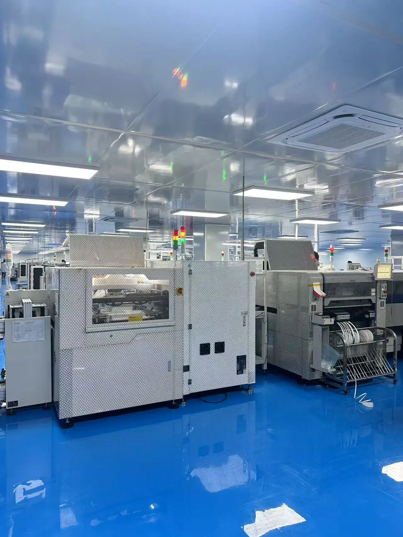
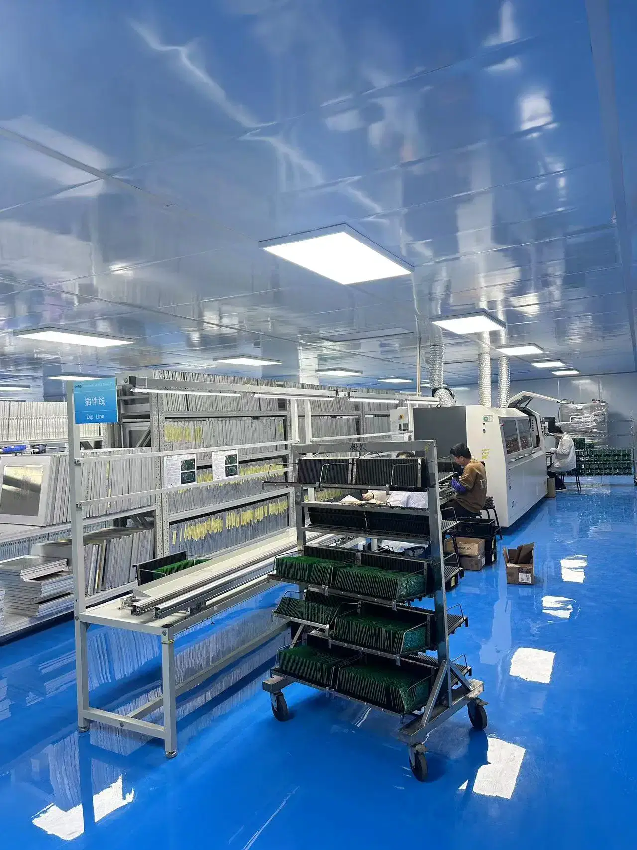
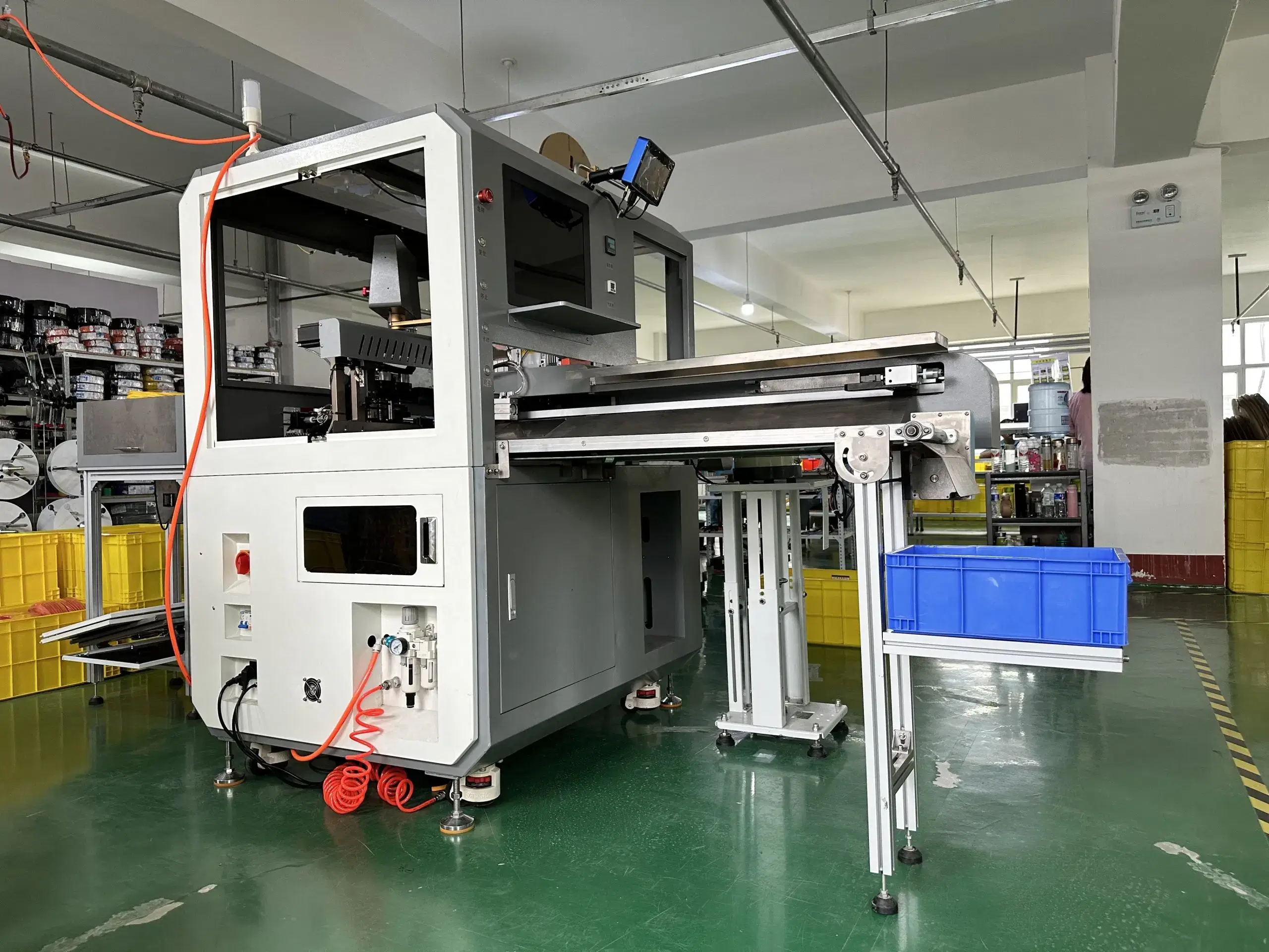
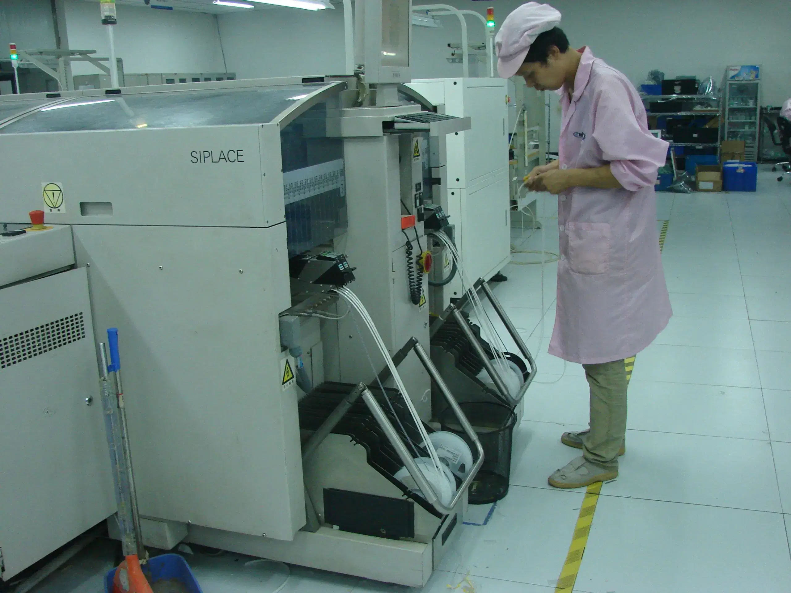
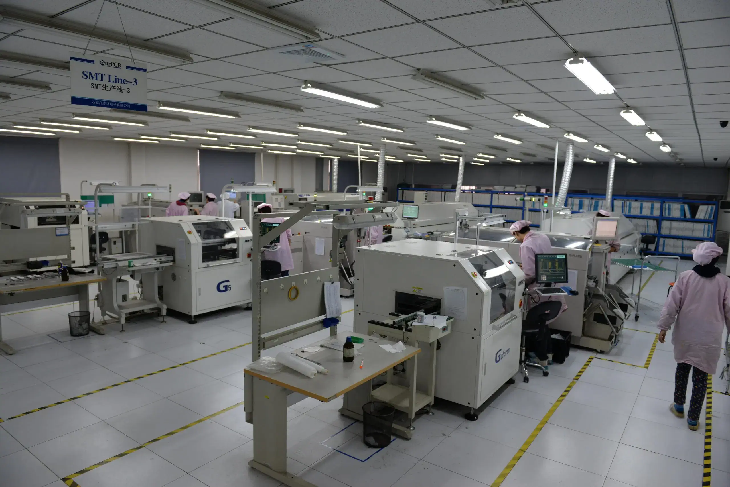
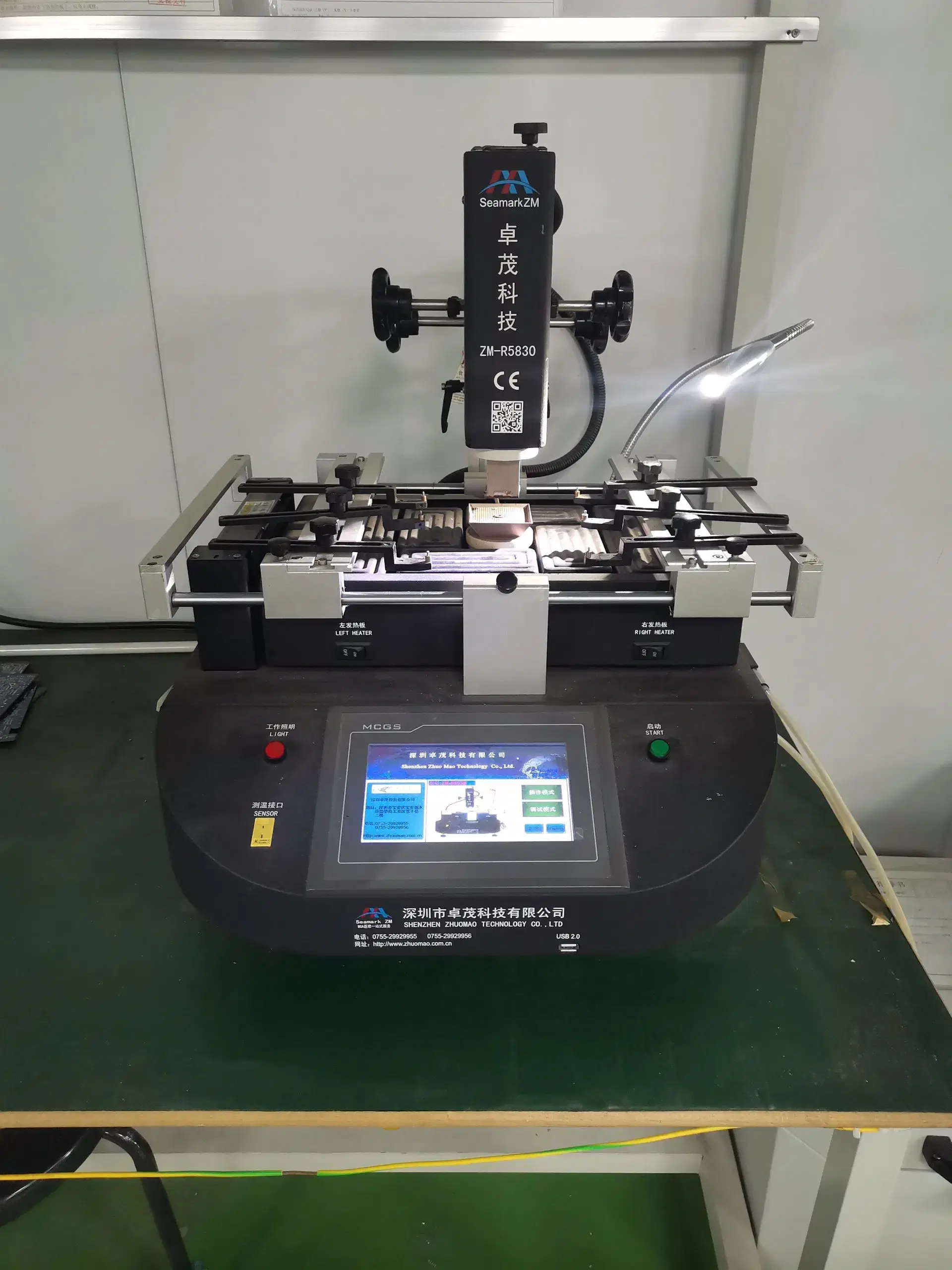
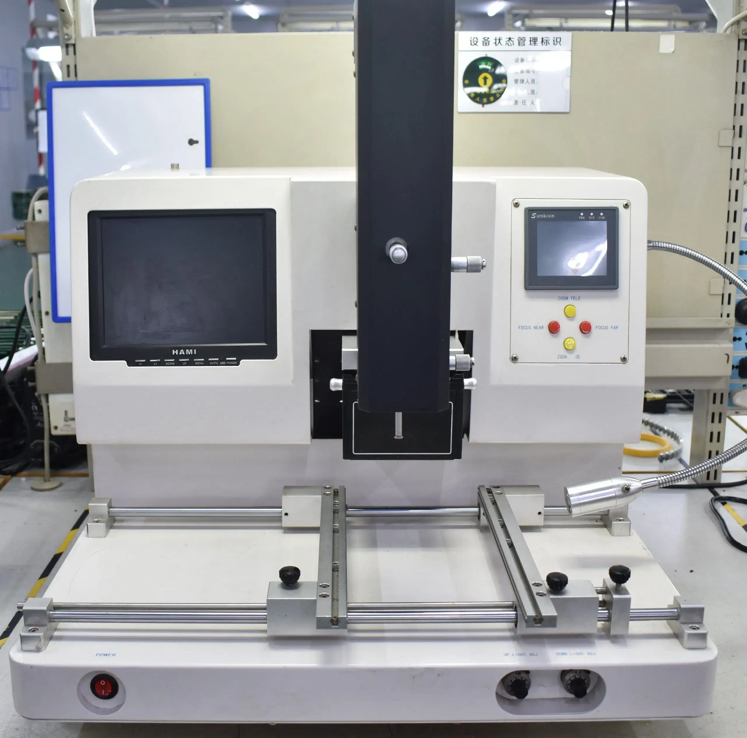
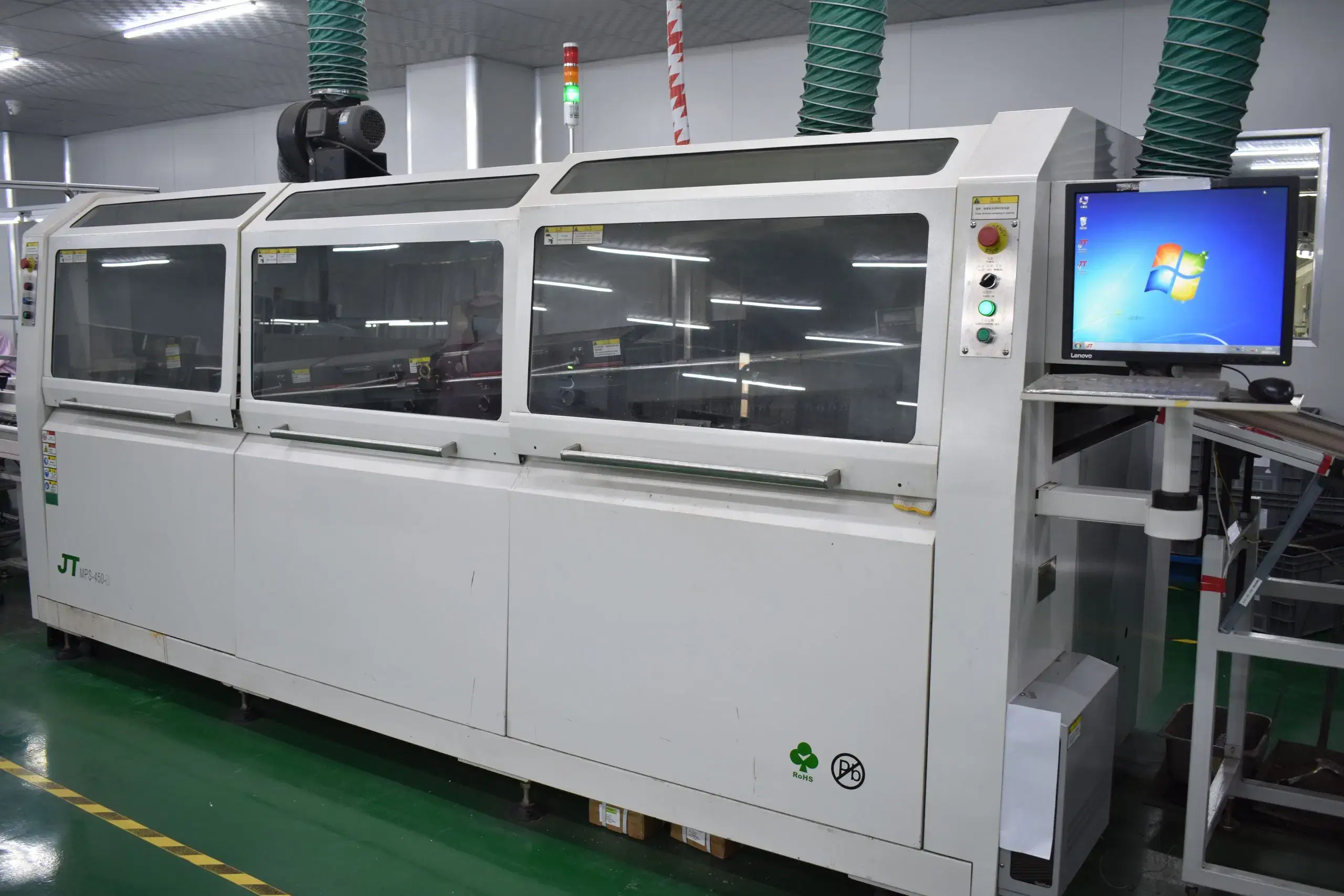
Our PCB Factory Gallery

FAQ
The full form of PCB is printed circuit board. A PCB in the telecommunications industry carries RF, power, control, assembly, and test needs that are much more stringent than a basic interconnect board.
A 5G PCB is not an independent category of fabrication. A 5G PCB is a type of high-frequency PCB built for 5G-specific bandwidth, frequency, loss, antenna, and testing, where the majority of the fabrication materials and process knowledge are the same.
Yes, provided that the manufacturer is capable of handling the required materials, precision features, performing RF testing, producing laminate, HDI, and conducting other required testing.
The design of 5G PCBs normally leverages high-frequency EDA and RF/microwave simulation capabilities, and typically does not require proprietary-only tools for 5G-based designs. The importance of impedance, S-parameter, and thermal simulations has more significance than the brand of software used.
Some defects can be reworked, when they are detected at the component level using either AOI (Automated Optical Inspection) or E-Test (Electrical Test). It is more challenging to rework RF-sensitive sections of a PCB, because the reflow or rework process may cause a shift in impedance, disturb hidden joints, or damage low-loss dielectric materials such as PTFE; high-value critical RF failures are often replaced rather than reworked.