Upload BOM & Gerber
-
Mobile: +86 13312967631
-
Email: sales@sugaintl.com

Multilayer PCB
Custom Multilayer PCB Manufacturer in China: From Stackup to Final Acceptance
Rigid multilayer PCB production with controlled stackups, registered inner layers, plated interconnections, and verified bare-board results.
Up to 40 layers SUPPLY RANGE
1.8/1.8 mil INNER FEATURES
40:1 THROUGH-HOLE ASPECT RATIO
What Is a Multilayer PCB?
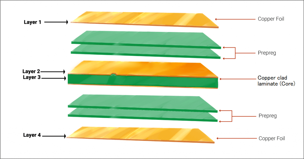
A multilayer PCB consists of multiple copper layers and dielectric materials, including cores and prepreg. The individual signal, ground, and power layers serve different electrical functions, while the various types of vias connect selected layers. The combination of the internal conductive elements, and not just the overall thickness of the PCB, distinguishes a multilayer PCB from a double-sided PCB.
Layer Functions and Interconnection
Signal layers carry routed interconnections. Ground layers provide continuous return paths for signals, while power layers distribute power supply rails throughout the PCB. By using more internal routing layers, the PCB can have greater interconnect capacity without increasing the area of the PCB itself. Using separate dedicated planes for power, digital, analog, and RF functions reduces the potential for unintended coupling between functions.
The various types of vias allow connections between layer pairs. Through vias run through the full depth of the PCB, while blind, buried, and microvias limit connections to selected layers. Each transition from one layer to another affects routing area, plane clearance, registration, and the finished vertical interconnection. Pad fields and barrel geometry must also be considered in the PCB stackup and drilling plan; these features cannot be treated as isolated connection symbols.
Core and Prepreg Roles in the Stackup
The core of a multilayer PCB is cured laminate with copper foil on one or both sides. Prepreg is used to bond cores and copper foil during lamination and creates the dielectric spacing after curing. The copper in the multilayer PCB is used for routed circuitry or plane layers.
The combination of core and prepreg forms a single electrical and mechanical structure. Dielectric spacing affects impedance geometry, copper distribution affects mechanical balance, and the reference layer provides a return path for signals. A routed trace can lose the nearby return structure assumed in the design if it crosses a split or gap in the PCB. For this reason, the manufacturing stackup needs to define both the electrical roles of the layers and the physical construction of each layer.
Multilayer PCB Compared with a Double-Sided PCB
| Structural feature | Double-sided PCB | Multilayer PCB | Engineering implication |
|---|---|---|---|
| Substrate structure | One substrate | Multiple cores and prepreg dielectric layers | Dielectric selection, lamination, and thickness control become part of fabrication. |
| Conductive layers | Two conductive sides | Multiple conductive layers | Internal routing and dedicated plane layers increase interconnect capacity. |
| Layer connectivity | Mainly top-to-bottom plated holes | Through, blind, buried, or microvia connections between selected layers | Registration, hole formation, and plating must match the layer-access plan. |
| Hidden circuitry | None inside the substrate | Inner copper becomes inaccessible after lamination | Inner-layer AOI is required before the structure is bonded. |
How Stackup Architecture Determines Layer Count
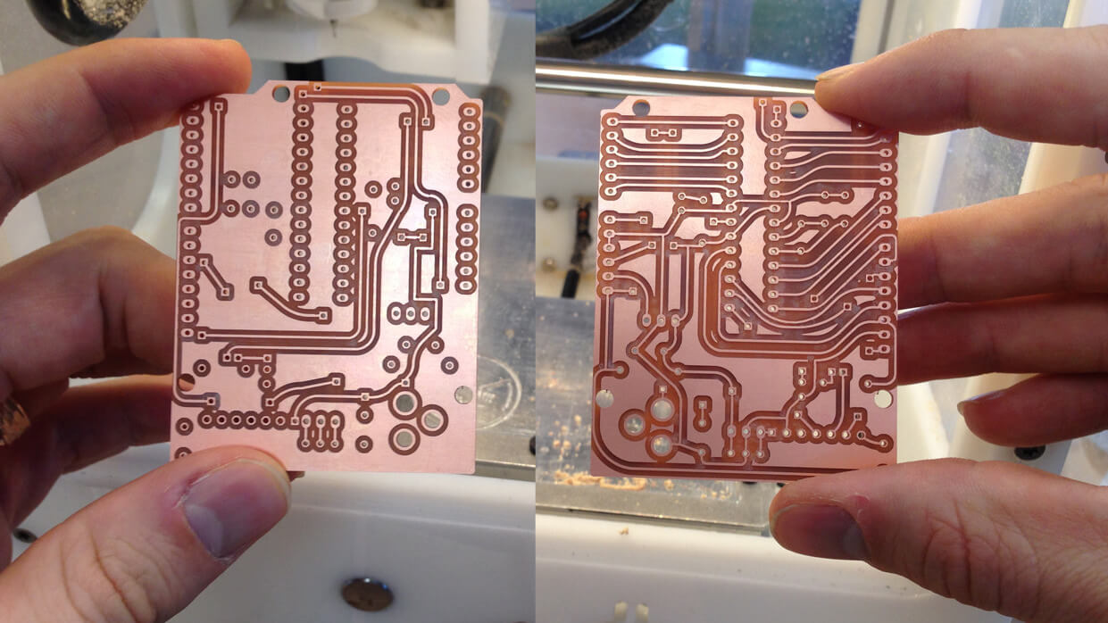
Routing density, reference-plane continuity, power domains, shielding, BGA escape, and mechanical constraints will determine the number of layers required. A four-, six-, or eight-layer pattern can serve as an initial guide, but the final stackup must define an electrical or mechanical function for each copper layer.
How Many Layers Does the Design Need?
Consider the component placement, pin fields, connector arrangement, board outline, mechanical thickness, power domains, and the need for controlled channels. Define each layer’s task. Generally, the outer layers are designated for component access and short signal paths. The internal signal layers add routing capacity to the design. Continuous ground and power layers support return current and distribute power to the circuit.
Four layers can establish dedicated signal, ground, and power functions. Six layers can expand the routing space or add another reference opportunity. Eight layers can separate more signal regions and power domains while still maintaining continuous return paths. An example of the overall layout of the PCB is Signal / Ground / Signal / Power / Power / Signal / Ground / Signal. However, the final layout of the PCB will need to follow both the circuit design and fabrication constraints.
An eight-layer PCB should only be considered when adding another layer pair solves a specific problem related to routing, shielding, power, or return-path constraints. Relocating components, rearranging pin assignments, reusing planes, or changing the via strategy may solve these problems without increasing the layer count.
- Determine the routing density, BGA escape, controlled channels, power domains, shielding, thickness, and connector placement requirements.
- Assign outer signal access, internal routing, reference layers, power distribution, and isolation requirements to the layers.
- Evaluate whether the constraint can be resolved through placement, pin assignment, plane reuse, or via changes.
- Add layers only when the remaining constraint requires a separate function.
- Validate the stackup, materials, copper, via access, impedance layers, finished thickness, and acceptance criteria before fabrication.
Stackup Balance for Warpage Control
While an electrically valid PCB stackup may not have a major warpage issue, some warpage may still occur due to the uneven distribution of dielectric thicknesses and copper weights within the PCB stackup during lamination and cooling.
The layout should have comparable copper layers paired symmetrically around the centerline of the PCB stackup, and dielectric constructions should also be paired symmetrically where possible based on the electrical design. The layout should also balance large copper plane areas against dense routing regions within the PCB stackup. When determining the balance between a large copper plane area and a dense routing region, resin flow, final finished thickness, PCB panel size, tooling, and the lamination plan must all be taken into account together with the copper distribution.
The word “symmetrical” does not mean that every copper layer in the PCB stackup has to be identical; it means that the PCB stackup has a controlled mechanical counterpart around the centerline. The final PCB stackup must document the electrical roles, dielectric thicknesses, copper weights, and copper-area balance together rather than presenting the electrical and mechanical requirements as separate decisions.
When Does a Multilayer PCB Outperform a Simpler Board?
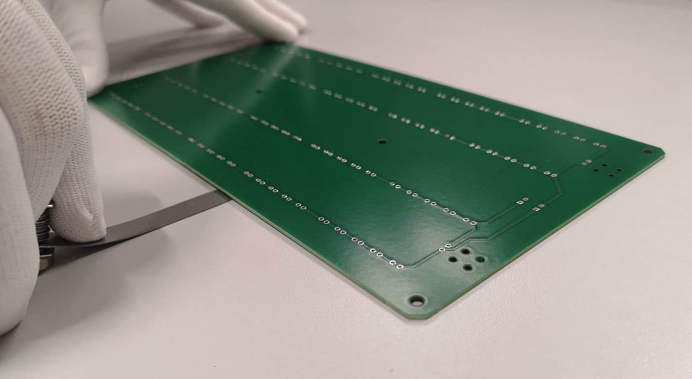
A multilayer PCB can use internal planes that assist in maintaining stable return paths and power distribution, internal routing that relieves dense escape regions, and separated layers for power, digital, analog, and RF functions to reduce coupling between them.
Retain a simpler, double-sided PCB when the routing fits, reference paths remain intact, power distribution is straightforward, and the PCB does not need internal layers for shielding or integration. Every additional layer adds manufacturing stages, hidden copper structures, inspection requirements, and reduced direct repair access. Each added layer needs a defined purpose.
How Material Selection Shapes Copper Construction
The materials selected for a laminate stackup must be defined as part of the stackup because the dielectric behavior, thermal expansion, resin flow, copper adhesion, and compatibility of each material with the lamination process affect the finished product together. Dk and Df influence controlled-channel geometry and loss, while Tg, Td, Z-axis expansion, and CAF resistance address different thermal and reliability risks.
The exact laminate and prepreg grades must be determined before the lamination parameters and impedance geometry are released.
| Material family | Multilayer PCB use | Stackup and manufacturing consideration |
|---|---|---|
| Standard FR-4 | General digital, control, and cost-sensitive products | Use the exact laminate grade, glass style, resin content, and dielectric thickness defined in the stackup. |
| High-Tg FR-4 | Repeated thermal exposure, lead-free assembly, and higher-temperature applications | Match the resin system, desmear, lamination profile, and plated-hole requirement. |
| Panasonic MEGTRON 6 family | Long digital channels, switches, routers, and backplanes | Define the exact laminate and prepreg grade, dielectric thickness, copper roughness, glass style, and coupon representation. |
| Rogers or hybrid construction | RF and mixed RF/digital multilayer boards | Define the compatible bonding system, material interfaces, lamination profile, and impedance layers before fabrication. |

Copper Weight in Fabrication
Starting copper is the foil present before imaging and plating. Finished copper includes copper added during subsequent process steps where applicable. Confusing the two can result in incorrect assumptions about trace width, spacing, annular rings, or finished thickness.
| Copper construction | SUGA capability | Best fit | Multilayer manufacturing effect |
|---|---|---|---|
| 0.5 oz inner copper | 17 μm starting copper | Fine signal routing | Supports finer inner features under the applicable imaging and etch window. |
| 1 oz inner copper | 35 μm starting copper | General signal and plane layers | Provides a practical baseline for mixed routing and plane functions. |
| 2 oz inner copper | 70 μm starting copper | Higher-current internal planes | Requires wider compatible features and stronger etch compensation. |
| Heavy copper construction | Up to 1000 μm in verified heavy-copper, embedded-copper, busbar, or copper-coin constructions | Power conversion and high-current distribution | Requires wider spacing, resin-fill planning, copper balance, compatible interconnects, and construction-specific thickness control. |
Higher copper weight also changes heat spreading and the via-pad geometry around plated interconnections.
Electrical Paths Within the Stackup
The configuration of electrical paths within the stackup depends on layer order, dielectric spacing, copper geometry, reference continuity, and finished registration. These paths must be defined with the stackup and reviewed against the same manufacturing data.
Reference Layers for Impedance
Without the reference layer, trace width, copper profile, dielectric height, material assumption, solder mask, tolerance, via transitions, and coupon definition, the impedance target is incomplete.
Etch compensation and dielectric control help keep the fabricated geometry aligned with the model. When defining channels, all layer transitions must be considered. For example, pad fields, plane clearances, and unused barrel length can limit a route that meets its target on straight trace sections. A same-panel coupon or representative production geometry provides the measurement basis when controlled impedance is specified.
Via Access and Stub Length
Through vias cross the full thickness of the board and depend on finished thickness, hole diameter, annular ring, desmear, and plating distribution. Blind and buried vias connect selected layer groups, while laser microvias provide access to adjacent or staged layers when package escape cannot use a conventional through-hole structure.
Blind, buried, and staged microvia structures may require sequential lamination because their interconnections must be completed before later layers make them inaccessible. A conventional through-hole structure requires no additional lamination cycle, while each staged blind, buried, or microvia interface requires a complete lamination-inspection-metallization cycle before the next layer group can be added. Therefore, in many cases, the cycle count rather than the via type affects cost and lead time.
Via-in-pad and backdrilled structures require specific fill, cap, and stub requirements.
Multilayer PCB Manufacturing Process
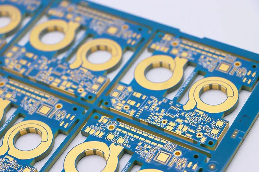
The multilayer PCB manufacturing process converts separate inner-layer images and dielectric materials into one registered electrical structure. A standard through-hole construction follows one main lamination cycle; however, blind, buried, and staged interconnections require partial lamination, inspection, metallization, and additional cycles before returning to the main manufacturing flow.
| Fabrication operation | Fabrication activity | Failure mode controlled | Accepted output |
|---|---|---|---|
| 1. Stackup and manufacturing data | Define layer order, dielectric system, copper, impedance layers, via access, and fabrication requirements | Missing or contradictory manufacturing inputs | Manufacturing stackup |
| 2. Inner-layer imaging | Transfer circuit images with controlled imaging | Image distortion, feature shift, and registration error | Imaged inner-layer cores |
| 3. Etching and inner-layer AOI | Etch copper and inspect opens, shorts, spacing, nicks, and pattern integrity | Hidden copper defects after bonding | Accepted inner-layer set |
| 4. Layup | Align materials, tooling, copper balance, resin system, and orientation | Misregistration, incorrect material, resin-flow imbalance, and trapped air | Lamination book |
| 5. Vacuum lamination | Apply controlled heat, pressure, vacuum, cure, and cool-down | Voids, delamination, thickness drift, bow, and twist | Bonded multilayer panel or partial build-up |
| 6A. Base drilling | Mechanically drill through holes, tooling holes, and specified controlled-depth features | Smear, breakout, positional error, and annular-ring loss | Drilled base panel |
| 6B. Sequential build-up | Form selected blind, buried, or microvia connections before the next lamination stage | Registration accumulation, fill defects, and interface failure | Completed staged interconnect |
| 7. Desmear and activation | Remove resin smear and prepare interfaces for metallization | Weak hole-wall adhesion and incomplete interconnection | Activated hole walls and via interfaces |
| 8. Copper deposition and plating | Form conductive seed and plated copper through holes and selected vias | Thin copper, plating voids, nodules, and poor adhesion | Metallized vertical interconnects |
| 9. Outer-layer formation | Image, plate, etch, and inspect final outer circuitry | Feature variation and surface pattern defects | Completed outer circuitry |
| 10. Solder mask and marking | Apply solder mask, legend, and required identification | Mask registration, exposed copper, and marking error | Protected board surfaces |
| 11. Surface finish and profiling | Apply the selected finish, route or V-score, clean, and check dimensions | Finish incompatibility, dimensional error, burrs, and contamination | Finished boards or arrays |
| 12. Final acceptance | Perform visual, dimensional, structural, and netlist electrical checks | Undetected structural or electrical nonconformance | Inspection and acceptance records |
Inner-Layer AOI Before Lamination
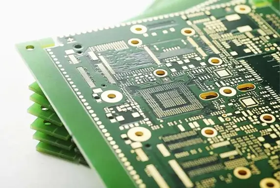
Prior to the lamination process that conceals the copper, inner-layer AOI is conducted to check for defects such as open circuits, short circuits, nicks, spacing variations, pattern distortions, and registration shifts. Any affected cores can be rejected or remade before the lamination process. Although AOI results indicate acceptance of the inspected copper patterns, these results do not validate dielectric spacing, resin fill, interlayer bonding, or final drill-to-pad registration; these conditions are confirmed after the lamination process based on dimensional checks, X-ray registration data, microsection analysis, and electrical testing results as needed. A record of the AOI results remains linked to the stackup revision and layer set used during the lot run.
Sequential Lamination for Hidden Interconnects
The method of creating a multilayer PCB using single-cycle construction results in a finished multilayer PCB consisting of a complete bonded layer set through which the holes are drilled. When using sequential lamination, selected blind, buried, or microvia interfaces are formed and verified prior to adding the next group of layers through additional lamination cycles. If an earlier stage creates incomplete fill, poor planarity, or an asymmetrical structure, these defects can be sealed within the subsequent laminations. In contrast, stacked microvias place increased demands on interface quality and alignment compared with staggered microvias because registration errors have a greater negative impact on stacked structures, even when the nominal laser-hole diameter is the same.
Plated Hole Formation
For the formation of plated holes, through holes and other specified features are created in the bonded panel using mechanical drilling. The desmear process exposes the internal copper connections, while activation and electroless copper are used to create conductive seed copper. Electrolytic plating then adds the required copper to form the barrel copper within the holes.
Assessments should be performed on the finished thickness, hole diameter, annular ring, copper distribution, and registration together, as the copper added by the electrolytic plating process reduces the original hole opening by adding copper to the drilled hole walls. If the basis for an aspect-ratio or annular-ring calculation is incorrect, the calculation may appear accurate on the calculation form, but the actual plated hole may contain less wall copper than anticipated by the designer. This discrepancy may not be detected until a microsection evaluation is performed. For high-aspect-ratio work, the approved manufacturing definition ties the calculation to plating thickness, microsection locations, and reliability requirements.
How Multilayer PCB Inspection Supports Acceptance
Acceptance or verification of a multilayer PCB structure requires consideration of inner-layer copper pattern integrity prior to lamination, finished-net continuity and isolation, plated-hole and microvia condition, controlled-impedance performance, and final dimensional and traceability requirements.
| Requirement | Inspection or test | Acceptance focus | Available record when specified |
|---|---|---|---|
| Inner-layer pattern integrity | Inner-layer AOI | Opens, shorts, spacing, nicks, pattern shape, and registration before lamination | AOI result linked to the lot and layer set |
| Finished network continuity and isolation | Flying-probe or fixture bare-board electrical test | Finished nets match the specified netlist and continuity/isolation criteria | Electrical-test result by board or lot |
| Hole-wall, via, and registration integrity | Microsection / cross-section | Copper thickness, plating voids, barrel condition, via interfaces, dielectric spacing, and layer alignment | Cross-section images and measurements |
| Controlled impedance | TDR on same-panel coupon or representative geometry | Measured profile meets the specified target and tolerance | TDR trace linked to the panel and stackup |
| Final board acceptance and traceability | Visual, dimensional, structural, and electrical checks | IPC-6012F Class 2/Class 3, order-specified addendum, IPC-A-600M, and order requirements | Inspection record, material identity, lot trace, and CoC when specified |
Why the Checks Are Not Interchangeable
Checks associated with inner-layer AOI, electrical testing, and microsectioning are fundamentally different because they answer different questions. For example, a passing netlist test provides no information about the physical condition of a plated barrel. In contrast, while a clean microsection may indicate that there are no flaws in the inspected location, it does not represent the entire production lot. TDR testing is used to check whether a controlled channel meets its target impedance, but it cannot replace network continuity testing.
The acceptance documents detail the hidden structures and electrical requirements specified for the actual multilayer construction. IPC-6012F Class 2 or Class 3 requirements, any order-specified addendum, IPC-A-600M, and relevant methods listed in IPC-TM-650 apply when identified in the procurement documentation.
Material identity, stackup revision, inspection records, electrical records, and lot traceability must connect the accepted structure to the delivered boards. Customer-facing reports, coupon traces, cross-section images, or CoC must be supplied when specified in the purchase order.
Multilayer PCB Manufacturing Capabilities
SUGA accepts multilayer PCB projects through SUGA-managed production or qualified partner capacity within China’s PCB supply chain and within the manufacturing windows specified below. The appropriate production arrangement will be confirmed during DFM and quotation, and SUGA will remain responsible for stackup alignment, supplier coordination, inspection, traceability, and delivery. The values stated below are available manufacturing limits and do not mean that every maximum can be manufactured on a single board. Feasibility will be determined by board size, material system, copper distribution, hole structure, finished thickness, registration plan, and required acceptance criteria.
| Requirement | SUGA capability | Manufacturing conditions | Verification |
|---|---|---|---|
| Layer count | Up to 40 layers | Single-cycle or sequential multilayer lamination. Maximum layer count depends on board size, material system, copper distribution, total thickness, via structure, and registration plan | Stackup, inner-layer AOI, registration, microsection, and electrical records |
| Inner trace / space | Down to 1.8 / 1.8 mil | Fine-line imaging, etch compensation, and controlled inner copper. Thin copper and controlled panel/design conditions are required; not a heavy-copper same-layer value | Inner-layer AOI and dimensional inspection |
| Outer trace / space | Down to 2 / 2 mil | Outer-layer imaging, plating, and etch compensation. Final copper, surface finish, and feature density affect the result | Outer-layer inspection and dimensional data |
| Mechanical drill size | Down to 0.1 mm tool size | Precision drilling, desmear, and plating. Tool size is not finished-hole size; board thickness, annular ring, plating, and aspect ratio interact | Hole inspection, microsection, and electrical test |
| Laser microvia | 3–6 mil (0.075–0.15 mm) | Laser drilling, metallization, fill/cap, and staged build-up. Dielectric thickness, capture pad, stacked/staggered structure, and fill integrity define feasibility | Microsection and electrical results |
| Finished board thickness | 0.1–12 mm | Thin-board handling through heavy rigid multilayer processing. Layer count, copper, panel support, connector needs, and flatness interact | Dimensional and flatness inspection |
| Copper thickness | Up to 1000 μm in verified heavy-copper, embedded-copper, busbar, or copper-coin constructions | Heavy-copper etching, plating, lamination, or embedded-copper integration with copper balance. Maximum copper does not coexist with minimum fine features on the same layer; the copper formation method and layer location are confirmed during DFM. | Cross-section and copper-thickness measurement |
| Through-hole aspect ratio | Up to 40:1 | High-aspect-ratio drilling, desmear, activation, and plating. Up to 40:1 applies to qualified high-layer-count or backplane-style through-hole constructions; the quote states whether drilled or finished plated-hole diameter is used and defines plating, microsection, and reliability requirements. | Microsection and electrical test |
| Layer-to-layer registration | ±3 mil | Registration tooling and controlled imaging/drilling. Panel size, material movement, layer count, feature density, and sequential cycles affect registration | Registration and dimensional records |
| Blind and buried vias | Single-stage and multi-stage structures | Controlled-depth or laser drilling with sequential lamination. Layer access, cycle count, capture pads, material interfaces, and fill/plating define feasibility | AOI, microsection, and electrical test |
| Via-in-pad / via-in-via | Copper-filled or resin-filled, capped and planarized | Fill, plate, cap, planarize, and finish. BGA pitch, pad planarity, assembly process, thermal path, and fill type must be specified | Cross-section and surface inspection |
| Stacked and staggered vias | Supported staged HDI structures | Sequential build-up with controlled alignment and fill. Stacked structures carry tighter capture-pad and interface requirements | Microsection and electrical results |
| HDI build-up | 1+N+1 through 8+N+8; up to 18-layer any-layer HDI | Repeated lamination, laser drilling, metallization, and fill/cap. Any-layer HDI is distinct from a standard 40-layer through-hole multilayer construction; cycle count, capture pads, fill integrity, and registration define feasibility. | Stage-linked AOI, microsection, and electrical records |
| Backdrilling | Controlled-depth stub removal | Backdrill tied to layer geometry. Residual stub, depth tolerance, pad/plane clearance, and board thickness must be specified | Depth inspection and channel verification |
| Controlled impedance | 50Ω single-ended, 100Ω differential, and custom targets; ±5Ω below 50Ω or ±10% at/above 50Ω | Stackup modelling, fabrication compensation, and coupon production. Material, dielectric height, copper, etch, solder mask, and transitions define the result | TDR result defined by the channel requirement |
Multilayer Feature Windows
The layer count indicates the number of conductive layers in a single PCB and does not indicate the feature class or interconnect architecture. The processing windows for inner and outer traces vary because the outer copper surface goes through additional plating and finishing processes and has a thicker copper layer than the inner copper when it is etched. Even if a circuit board meets the inner-layer trace/space minimum during design, that same PCB may not meet the same minimum for the outer copper layer, as additional copper will be present when the outer layer is etched.
Compatible drilling, desmearing, activation, plating distribution, annular-ring control, and microsection or reliability evidence are required for high-ratio through-hole constructions. Material movement in a high-layer-count multilayer assembly creates additional registration challenges for PCB manufacturers. Therefore, even though a feature may be proven on a PCB that is thinner than a 40-layer construction, it may not be duplicated on a 40-layer construction without further review.
Combined Manufacturing Limits
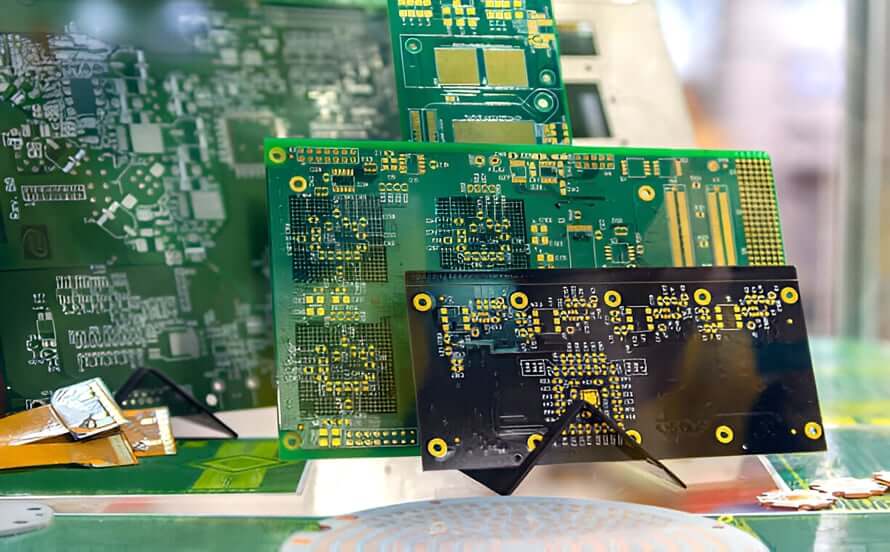
Fine-line features typically require thinner copper to allow for appropriate imaging and etching process windows, whereas heavy-copper features require wider spacing, resin-fill planning, compatible pads, and mechanical balance. Because of the interaction between the two design directions, DFM should analyze the actual configuration and parameters rather than the maximum limits of both designs individually. Each individual design feature—1.8/1.8 mil inner-layer features, 1000 μm copper construction, 0.10 mm mechanical drill, 12 mm board thickness, and 40:1 aspect ratio—has the potential to be manufactured. However, receiving and analyzing a stackup containing two or more elements of a combined construction will trigger a DFM review rather than a flat quotation.
What Drives Multilayer PCB Cost or Lead Time?
Why Layer Count Alone Cannot Set Price
Layer count alone will not give a definitive answer to the question, “What is the price of a 4-layer PCB?” Many factors need to be included when determining the price, including board size, material type, copper thickness, feature class, hole structure, finishing process, test coverage, manufacturing quantity, panel utilization, and intended schedule. Although the number of layers has some impact on manufacturing cost, the overall cost is primarily determined by usable panel yield and process complexity based on all of these inputs combined.
Other material types, such as low-loss and hybrid materials, require different manufacturing controls because of differences in thermal behavior and stiffness. Heavy copper requires more material, places additional demands on tooling and handling, and may require additional documentation compared with a conventional substrate. Tight registration, backdrilling, additional coupons, and extended reporting can also change process time, inspection effort, and documentation even when layer count is unchanged.
Why Lamination and Via Cycles Affect Lead Time
As the laminate layers and via structures are created for a PCB, each cycle must be completed and accepted before the next structure is added. Two PCBs manufactured with the same number of layers can have different schedules if one uses a single through-hole cycle and the other uses buried vias, stacked microvias, backdrilling, hybrid materials, or additional acceptance coupons during the manufacturing process.
Multilayer PCB Applications

Automotive and EV Systems
ADAS processors, battery-management controllers, infotainment, and mixed-domain vehicle electronics place sensing, digital communication, and power switching in one assembly.
Automotive electronic systems use high-current switching copper, low-noise return paths, dense routing traces, and connectors or load terminals, while also experiencing repeated thermal cycling. The copper planes, hole-wall copper, copper balance, stackup materials, and automotive acceptance requirements must be reviewed together.

Telecom and High-Speed Computing
Switch fabrics, optical modules, servers, backplanes, and base-station electronics use multilayer stackups to create controlled differential channels, maintain continuous reference planes, allow dense connector escape, and minimize vertical transition length. Risks include connector-launch discontinuity, glass-weave skew, via-stub resonance, low-loss material variation, and coupons that do not represent production channels. Backdrill depth, residual stub, copper roughness, dielectric spacing, and TDR geometry must all be managed together with the stackup used to create the finished product.

Medical and Healthcare Devices
Patient-monitoring equipment, diagnostic equipment, imaging equipment, and wearable health-monitoring devices use a combination of low-level analog acquisition, digital processing, power, and communication within a limited footprint. A risk is treating “medical PCB” as a material identifier rather than a controlled production record. Documentation for medical devices should include material identification, stackup revisions, plated-interconnect evidence, lot traceability, and any order-specified medical addendum. Traceability must match device risks and procurement requirements.
Industrial Automation and Control
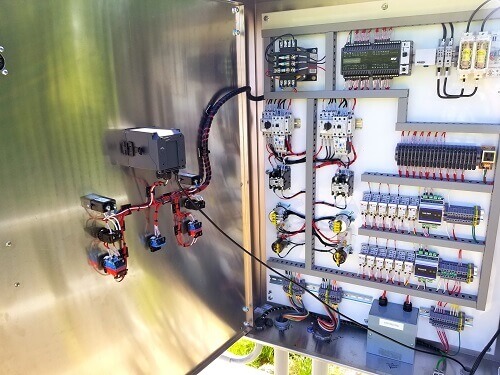
Motor-drive control circuits, PLC backplanes, sensor interfaces, and automation controllers employ multilayer planes and internal routing to separate switching, logic, sensing, and communication. For high reliability, long service life, or mixed high-current and low-level signals, review finished-hole tolerance, barrel copper, drill-to-copper clearance, and PCB flatness. Press-fit connectors and vibration further increase the importance of these controls. An eight-layer industrial control construction can use 1.8 mm finished thickness, 3/3.5 mil line/space, 0.2 mm minimum holes, 0.13 mm hole-to-line spacing, 1 oz outer copper, and ENIG; the released drawing must state whether 0.2 mm is the drill size or finished plated-hole diameter so aspect-ratio and annular-ring margins can be checked correctly.

Aerospace and Avionics
Avionics uses multilayer construction to integrate processing, RF, power, and sensor domains under mass and space constraints. Repeated thermal cycling, long service intervals, and restricted repair access increase the consequence of weak plated barrels, microvia interfaces, material movement, and accumulated registration error. Stackup symmetry, material control, microsection criteria, and the order-specified space or military requirements must be defined before fabrication.

Consumer and IoT Electronics
Consumer electronics, including smartphones, wearable devices, and gateways, as well as IoT products, use multilayer construction with selected microvia access to increase the number of interconnections within a limited physical space.
Some of the unique constraints of this type of construction are local warpage caused by thin-panel handling, antenna reference continuity, microvia cycle count, and stacked-interface reliability. Smaller laser holes do not by themselves create a safer construction, while inadequate capture pads, fill, planarity, or sequential registration can cause problems.

Energy and Power Electronics
Power converters and battery systems use multilayer constructions to separate control, gate drive, sensing, communication, and current-carrying paths while also combining electrical insulation with thick-copper topography. Copper up to 1000 μm requires verified heavy-copper, embedded-copper, busbar, or copper-coin constructions. This construction requires resin fill, copper balance, dielectric thickness, plated transitions, creepage distance, and clearance. These constraints cannot be solved by adding layers alone, and 1000 μm copper constructions require wider feature rules than fine-line signal layers.

Semiconductor Test and Measurement Equipment
Semiconductor test and measurement equipment routes many synchronized channels through load boards, interface boards, or data-acquisition instruments for precise component measurement. A high density of channels combined with high layer counts requires high levels of flatness, connector-registration accuracy, and via-stub control. Large board size, dense connectors, controlled channels, repeated insertion loads, channel-to-coupon correlation, and precise power and measurement functions must be reviewed together.
Test access must remain repeatable across the full interface, not only electrically continuous at final bare-board test.
Why Choose SUGA for Multilayer PCB Supply
As a Chinese multilayer PCB source, SUGA leverages over 30 years of PCB engineering experience with an integrated manufacturing network, allowing SUGA to manage your project at its facilities or through a partner qualified for the required layer count, materials, HDI, heavy copper, drilling, or inspection window. Through SUGA’s control of DFM, manufacturing data, supplier coordination, acceptance, and delivery, we provide clients with one source for commercial and technical support.
How Stackup Revisions Stay Aligned from Prototype to Production
The complete manufacturing package defines the layer order, material grade specifications, copper thickness, via access, drill data, impedance requirements, process notes, inspection, and acceptance methods. All conflicts are resolved before fabrication. The approved stackup revision will be used for production instructions and inspection records.
Prototypes submitted for production and scheduled production use the same controlled definition. It applies to any approved production changes. Changes to the factory, laminate, prepreg, via structure, or acceptance method will be reviewed against electrical, thermal, mechanical, compliance, and delivery requirements before release. Material identity, stackup revision, inner-layer AOI, microsections, electrical results, and specified coupon data will remain linked to the relevant board, panel, or lot.
Traceability After a Change or Failure
All fabrication files, stackup versions, drill data, material specifications, process notes, partner-factory records, and order documents will use the same revision. To prevent mixed revisions and undocumented substitutions, any proposed alternative material or process must be approved against the same electrical, thermal, mechanical, compliance, inspection, and delivery criteria. If an inspection or test identifies a failure, the affected lot will be contained, and the relevant production and traceability information will remain linked to the same production and traceability record originally supplied. The root cause, correction, retest, disposition, and closure must remain linked to it.
Our PCBA Production Lines
















Frequently Asked Questions
Delamination risk rises when there is a mismatch or variation in the laminate grades used to fabricate the PCB, the prepreg resin used to bond the layers, copper distribution, moisture condition during fabrication, lamination heat or pressure, and the vacuum and cure conditions applied during lamination. Drilling and desmearing can also affect the bonded interfaces surrounding plated interconnections. Prevention of delamination depends on using matched materials, controlling press conditions, maintaining copper balance, and tying structural inspection to the specified construction.
See Core and Prepreg Roles in the Stackup above—the two materials have different functions. When an engineering drawing changes either the core or prepreg grade after the initial stackup approval, the finished thickness will change even if the copper and layer count remain constant. Therefore, a revision with a “no electrical changes” note may still require a thickness or impedance check, even when the revision only involves a change in material grade.
Quote packages typically include Gerber or ODB++ data, NC drill and rout data, netlist data, stackup data, impedance requirements, material and copper requirements, via layer-access data, fabrication drawings, quantity, and test requirements. The quote package should also identify the revision, PCB outline, finished-hole dimensions, tolerances, surface finish, acceptance class, and required reports.
A microsection measures hole-wall copper, plating voids, barrel condition, via interfaces, dielectric spacing, and layer alignment. A question you may want to ask the supplier is, “Is the microsection taken from a coupon fabricated on the same panel as the actual boards, or from a separate reference build?” A supplier may provide a microsection from a different panel or lot that passes inspection while the shipped boards have plating or registration issues that the coupon could not detect.
Layer-to-layer registration is specified at ±3 mil. The practical implication is that using a pad or keepout area sized to the nominal registration tolerance without additional margin can cause a high-layer-count or stacked-via design to be flagged during DFM evaluation. Pad and keepout design should include margin against the stated ±3 mil registration tolerance rather than treating the tolerance as unused headroom.
The drill-tool diameter and finished-hole diameter differ because plating narrows the original opening. Before submitting an engineering drawing for quotation, ensure that every aspect-ratio-sensitive hole specifies the diameter basis used. If the drawing does not provide this information, the supplier may apply its default assumption, which may not comply with the specified reliability requirements. Plated and non-plated holes should also be identified separately because they have different tolerance stacks.