Upload BOM & Gerber
-
Mobile: +86 13312967631
-
Email: sales@sugaintl.com

PCB Design Services
PCB design and layout support from file review to manufacturing output
Send schematic, netlist, BOM, mechanical constraints, or existing layout files for engineering review, layout support, DFM, DFA, and fabrication or assembly outputs. SUGA provides additional support based on file condition, board technology, package requirements, and the output condition the engineering or production team needs to receive.
40-layer layout
0.2 mm BGA ball-to-ball gap
12 Gbps differential routing
±5% controlled impedance
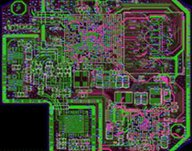
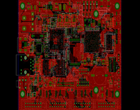
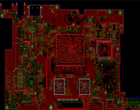
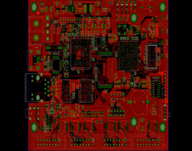
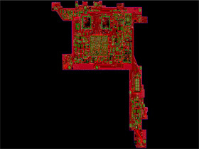
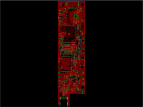
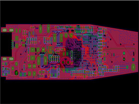
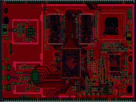
PCB LAYOUT SHOWCASE
What Are PCB Design Services?
PCB design services consist of engineering, layout, and manufacturing outputs that transform circuit intent into board data for production. The specific services provided depend on the current project state; for example, a circuit that is still changing requires design engineering, whereas an approved schematic can directly enter PCB layout. Likewise, existing layouts may require DFM review and a manufacturing output package instead of redesign.
A PCB designer turns electrical intent into a board that can be inspected, fabricated, and assembled by another party. Problems and complexity increase when package density rises, controlled impedance is required, mechanical limits are present, or incomplete files create interdependencies between decisions.
Design Engineering
Design engineering works upstream of physical routing to resolve the functional operation of the circuit, identify the components to be used, provide schematic logic, power requirements, interface behavior, and the constraints of the layout. During this design phase, routing too early when the schematic or BOM is still moving can mask an unresolved decision behind board geometry and lead to further design problems in assembly.
An engineering request should state whether SUGA is completing an engineering review of an existing schematic, correcting circuit documentation, completing the BOM, or assessing SI and PI requirements. It should also identify the sign-off authority for the electrical requirements, which separates circuit responsibility from layout execution.
Layout Service
Layout services convert approved electrical requirements into PCB design by generating component placement, trace routing, layer planning, and manufacturing data from this conversion. The PCB layout team requires consistent connectivity, mechanical boundaries, trace routing guidelines, and package specifications. PCB layout services do not automatically include circuit redesign. The PCB quotation identifies what happens when the supplied schematic contains incompatibilities with constraints or package information.
Layout deliverables include source files in editable format, Gerber data, fabrication drawings, and assembly-facing outputs included in the order.
| Aspect | Design Engineering | PCB Layout | Customer decision | Required input | Best next service |
|---|---|---|---|---|---|
| Focus | Circuit functionality and electrical design | Physical placement and trace routing | Engineering when circuit intent or components are still changing; layout when the electrical requirements are stable | Product requirements, schematic status, component constraints | Design review or layout quote |
| Starting point | Concept and schematic design | After schematic completion | An incomplete schematic requires upstream review; an approved schematic can enter placement planning | Concept notes or approved schematic, BOM and netlist | Engineering consultation or layout intake |
| Skills required | Circuit theory, electronics, SI | Spatial design, layout, manufacturability | Confirm whether the project needs SI/PI analysis, routing execution or both | Electrical constraints, mechanical envelope, interface requirements | Complex-layout review |
| Deliverable | Schematic and BOM | Gerber data and fabrication drawings | Confirm source-file access and downstream manufacturing files before ordering | Requested deliverable list and version format | Fabrication or assembly output |
The buying decision follows the files, not the service label. Any incomplete circuit requirements must undergo an engineering review before being placed into placement and routing; only upon approval of the requirements may the project proceed to placement and routing without returning to circuit decisions.
DFM Review and Manufacturing Output
A DFM/DFA review or manufacturing output will allow the project team to present a comprehensive overview of the previous board layout and identify the necessary adjustments without requiring extensive redesign work to complete the project. The DFM/DFA review provides a list of issues or decisions that must be made before producing a manufacturing-output package. The detailed DFM/DFA criteria are included in the design review section below.
PCB Design Inputs Before Quote
The only information available for quoting is that which is in the files: i.e., schematic status, BOM stability, connectivity, board outline, and design constraints. The design specifications provided allow SUGA to determine if the request is design engineering, PCB layout, review-only work, or manufacturing-output review. If any information is missing, the initial engineering task will be adjusted and, as a result, the pricing or schedule may need to be adjusted.
Minimum Files for Initial Quote
The minimum required files to begin quoting are the latest schematic or current PCB source/Gerber package, a BOM or component list, board outline, and requirement summary. If any of the documents are not available, it’s important to note what documents are missing. An older revision of the schematic should not be assumed without clarifying that it’s an older revision.
The initial package will provide answers to four questions: what items are already approved; what does SUGA need to design or review; what files does the customer expect; and what is the next production stage? This will provide enough information to proceed with the engineering review until further detailed constraints are submitted.
- The schematic or current board data establishes connectivity and design status.
- The BOM identifies package, sourcing assumptions, and assembly-sensitive parts.
- The board outline or DXF establishes usable area, mounting points, and interfaces.
- The requirement summary indicates the intended application, expected outputs, and known constraints.
Recommended Inputs for Layout Work
The recommendation is to confirm that the netlist, verified footprints and component Datasheets and mechanical data agree with the schematic and BOM before starting the layout. Placement considerations should also be made for: fixed connectors, keep-outs, height limitations, heat sources and critical component relationships. Routing needs to define controlled impedance nets, differential pairs, current paths, length rules and topology rules.
Extra Inputs for Complex Boards
High-speed and RF designs will include interface standard requirements, stack-up info, impedance values, reference layer plan requirements, and loss or validation requirements. Dense BGA and HDI designs require package drawings, ball maps, via preferences, escape assumptions and fabrication limits. Rigid-Flex PCB designs incorporate bend regions, flex stack-up, mechanical movement, and enclosure geometry.
Power, high-voltage and thermal PCB designs have additional information: current ratings, copper specifications, clearance specifications, heat and operational information. Changes to placement due to test access, connector behavior or limitations on how to assemble may reduce the placement area before routing commences. Providing all of these limitations upfront during the first review will prevent the quote for a complex PCB design from treating it as a regular PCB geometry.
PCB Design to Manufacturing Process
The PCB design and manufacturing process is as follows: File Intake > Engineering Review > Layout Planning > Design Check > Customer Confirmation > Manufacturing Output. If a DFM issue arises and routing reopens, you go back to that step instead of creating an unversioned routing file for manufacturing your PCB.

File Intake and Engineering Review
File intake begins with identifying the File and not determining whether or not it meets technical requirements. The engineer begins by recording the board number, revision number, date, and what files were supplied. Next, they determine if the schematic, BOM, netlist, outline, and constraints are from the same design state. If any of these files do not match at this point, the review process may be compromised even though each of these files opens properly.
Engineering reviews will produce a defined design task. That will include identifying which inputs were missing, which requirements were conflicting and need clarification, what outputs are expected or needed, and what manufacturing and assembly dependencies exist between them. From this process comes a short issue list that will be used to determine whether to continue with the current design, ask for more information, or define an upstream design task.
The procurement department uses this task definition to create a standard comparison of all quotations for the same work content. One supplier may only quote for the routing, whereas another will provide a quote that includes the electrical review, library corrections, and manufacturing coordination.
Layout Planning and Routing
The first step in planning routing is to have a stack-up, board outline and the critical interfaces. The layout engineer then starts by placing the fixed mechanical items first (e.g., connectors), then the components that control return paths, power flow, thermal behavior, or fan-out (e.g., relay pins). Routing priority will be determined based upon project constraints and not simply based on the generic sequence of each layer.
The layout plan will include a statement of the rules that come from the customer and the rules that are based upon the manufacturing requirements and the engineering assumptions. These rules are important when a particular via, material or layer is changed, as they may affect the impedance or escape routing of the routed paths.
The reviewable layout will show which choices will affect the end-product before the final checks begin.
Design Check and Customer Confirmation
The purpose of a design check is to find different ways that a product may fail. DRC checks for design rule and connectivity violations; DFM checks how the geometry of the PCB will relate to the limits of fabrication; DFA ensures the assembly can be built with the current footprints and orientation; SI/PI and electromagnetic reviews focus on return paths, impedance, power delivery, and sensitive interfaces if these services are included.
Findings are recorded and associated with severity and action items. A blocking issue requires a corrective action. A customer decision item may be manufacturable but needs to go through a risk assessment or cost approval. Items related to manufacturing and assembly are sent to the team responsible for that process.
PCB Layout Capabilities
Just because a PCB has a particular number of layers or feature size does not mean it is ready for quoting. The only way to determine if any information is suitable for quoting is to read the information against the stack-up, package data, material, impedance target, drill strategy, and manufacturing conditions that make the information useful.
Layout figures, fabrication figures, and assembly figures are for different jobs. Be careful to separate the units and roles before making a comparison between suppliers.
| Term | Meaning | Do not confuse with |
|---|---|---|
| Data rate (Gbps) | Serial interface data rate, such as 12 / 25 / 28 Gbps and 56 / 112 Gbps PAM4 | RF frequency (GHz) |
| RF frequency (GHz) | RF operating frequency, such as 60 GHz | Data rate (Gbps) |
| Ball pitch | Center-to-center distance between adjacent BGA balls, such as 0.4 mm fine pitch | Ball-to-ball gap |
| Ball-to-ball gap / spacing | Edge-to-edge clearance between adjacent balls, such as 0.2 mm spacing | Ball pitch |
| Ball diameter | Diameter of a single solder ball | Pitch / spacing |
| Pin / ball count | Total package pin or ball count, such as 2,912 | Layer count |
| Item | Capability | Engineering Condition |
|---|---|---|
| Max. layers (layout) | 40 layers | Stack-up and material confirmed with fabrication partner |
| Max. terminal count per board | 60,000 | Counting method (nets / component pins / routed terminals) confirmed before scheduling |
| Max. components per board | 3,600 | Package and placement data complete |
| Min. BGA ball pitch | 0.3 mm | Pitch, gap and diameter distinguished per term table |
| Min. BGA ball-to-ball gap | 0.2 mm | Package drawing and escape strategy supplied |
| Max. BGA ball count (single package) | 2,912 | Full ball map, package drawing and net assignment supplied |
| Max. BGA packages per board | 48 | Package mix and escape strategy planned across layers |
| Min. trace width / spacing | 2.0 mil / 2.0 mil | Down to 1.8 mil with confirmed copper weight and fab-house DRC |
| Min. hole aperture | Mechanical drill 6 mil; laser drill 4 mil | Via technology and aspect ratio defined |
| Highest validated channel rate | 12 Gbps differential baseline; 25 / 28 Gbps on review | Interface standard, stack-up, material and channel-loss budget supplied |
| ELIC / any-layer HDI | Supported as interconnect structure | Build-up, via stack, laser-drill capability and lamination cycle agreed with fab house |
High-Speed and Controlled-Impedance Layout
High-speed and controlled-impedance layout and design need to be analyzed according to the performance targets of a particular system. When implementing high-speed designs for 12 Gbps, 25 / 28 Gbps or 56 / 112 Gbps PAM4 channels, engineers must consider the topology, stack-up, material selection, signal return paths, length and attenuation performance characteristics, and build/test coupon methods that meet performance requirements, depending on the amount of control and consistency provided during the manufacturing process.
Controlled-impedance layout design must follow the same logic as high-speed designs. A controlled-impedance target of ±5% can only be achieved if the design defines the geometry, copper thickness, materials, and test procedures for controlled-impedance testing.
SUGA works closely with the manufacturing source to provide all routing criteria, evaluate the necessary laminate stack-up, and prepare fabrication data.
HDI and Fine-Pitch BGA Layout
Fine-pitch layout design converts the information obtained from the package analysis into a series of via and escape decisions based on package specifications. The quote includes any necessary details regarding whether 0.2 mm represents a ball-to-ball gap, whether 0.3 mm represents pitch, or whether 2,912 represents the ball or pin count associated with the package.
The ball map, package drawing, layer target, via structure and assembly clearances will all dictate routing requirements.
In addition, ELIC and any-layer HDI designs will require the intended build-up stack, via stack, laser-drill capabilities, and lamination cycle for production. SUGA will review all dependencies against manufacturing requirements to ensure that the choice of interconnects relates to a producible laminated stack, and not evaluate ELIC as a separate line item/price item.
Rigid-Flex and RF Design Support
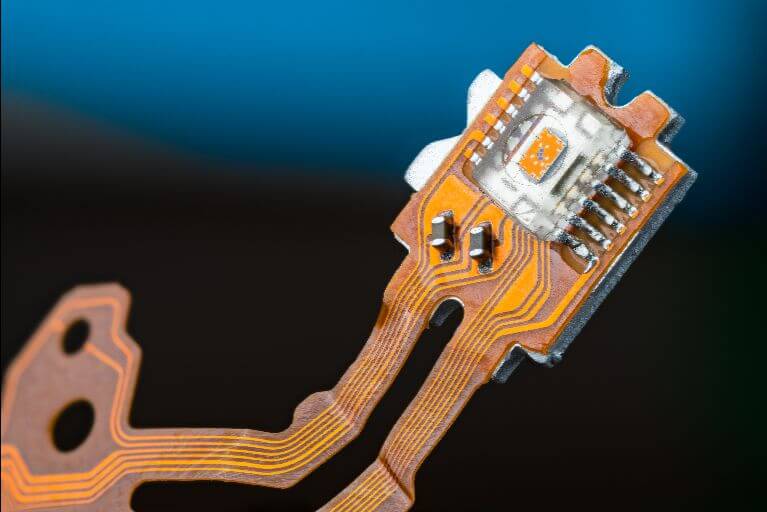
Rigid-flex layouts are created around mechanical movement. Flex zones, bending radius, layer transitioning, stiffeners, keep-outs, and enclosure geometry determine placement and routing of components before a board is moved to the manufacturing stage. The material and stack build-up should accommodate these decisions.
When conducting RF work, the focus is on frequency, material, geometry, and return path. RF at 60 GHz is not the same as a serial data rate. Evaluating the design includes examining the transmission structure, grounding, transition points, and the test environment for the manufacturing package.
Design Tools and Mixed Technologies
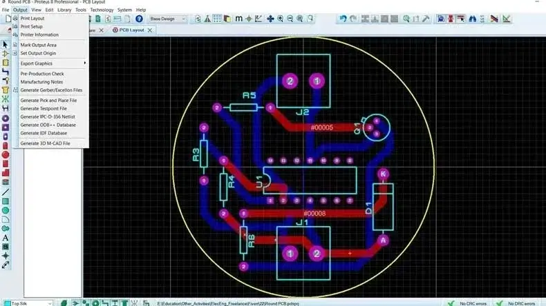
The compatibility of software tools helps SUGA accurately receive, modify, analyze, and send the design back to you. Cadence Allegro, OrCAD Capture, PCB Designer, PADS, HyperLynx, Altium Designer, Eagle, and P-CAD files must be supplied with their native sources, libraries, and versioning. Converting from one tool to another may preserve some of the geometry but not the design constraints or library intent of the original file. As such, the quote for conversion should specify which deliverable will remain modifiable.
Mixed digital, analog, RF, and power boards require different rule groups and review process priorities.
PCB Design Review and DFM Checks
Before a PCB can be manufactured or assembled, all relevant DRC, DFM, DFA, Stack-up, Impedance, Electrical, Thermal, Mechanical, and EM checks must be performed, and the results recorded. Each check should have an Input and a Risk Output. Free file checks may identify obvious intake issues, but are not as comprehensive as an engineering review.
DFM and DFA Review
A DFM check compares the characteristics of the PCB with the manufacturing process. Trace widths and spacings, drill size, copper thickness, stack-up, solder mask, panel configuration, and special manufacturing processes can influence whether or not the geometry is feasible. The output contains the name of the feature being checked, the file that contains it, the process dependency, and any required adjustments or confirmations.
A DFA evaluation assesses the assembly package. Footprints, polarity, orientation, component clearance, placement access, soldering, inspection, testing, and rework depend upon information external to the routed copper. A PCB may clear the fabrication review and still result in questions regarding assembly; thus, DFM and DFA checks are connected but not synonymous.
DRC Checks
DRC checks for connectivity, clearance, creepage, trace, via, and rule violations within the design environment. Reports summarize both actual rule failures and documented project exceptions. Reports will also identify the source-file version and rule set used; if this is not included with a clean report, it may reference an incorrect design state.
IPC-2221B establishes broad printed-board design standards and land-pattern requirements follow IPC-7351B with the sanctioned project standard and package data. Fabrication and assembly reviews must still be conducted on a project because a CAD rule may not define every supplier condition.
When using a consistent severity model, managing risks is more straightforward.
| Issue type | Meaning | Output |
|---|---|---|
| Blocking issue | Cannot proceed to fabrication or assembly as-is | Engineering question / required change |
| Customer-decision issue | Manufacturable, but cost or risk needs customer approval | Decision note / approval |
| Fabrication issue | Requires fabrication capability confirmation | Fabrication capability check |
| Assembly issue | Affects placement, soldering, test or rework | Assembly review note |
This classification provides the project team with information on who will be responsible for closing each item. In addition, it prevents a supplier-dependent question from becoming an exception that customers approve without proper scrutiny.
Stack-Up and Impedance Review
The stack-up review verifies that the layer assignments, reference planes, material assumptions, copper, and manufacturing capabilities are appropriate. SUGA reviews the return paths and geometry and compares these to the proposed stack to verify that they are suitable for manufacturing, and fabrication-dependent values will remain explicit assumptions until the build has been confirmed.
The impedance review establishes the electrical target and associated tolerances to the proposed stack. The engineer documents the target specification and tolerance, geometry, reference plane, and measurement method. When any routing or material changes occur, the associated traces must go back for re-evaluation rather than being continued with an obsolete calculation.
Electrical and Electromagnetic Checks
The electrical review of a design verifies that the power sources, return paths, interface connections, and areas that conduct high current are connected properly and function under the conditions stated in the schematic and constraints. The electromagnetic review of the design checks whether there are any issues with the routing paths, reference planes, sensitive circuits and signals, clocks, connectors, and coupling paths in the layout; these checks will reveal design risks but are not intended to replace laboratory-compliance testing.
Thermal and mechanical aspects are reviewed in the same step when supplied. This includes checking heat paths, mounting points, edges of enclosures, forces of connectors, and any 3D interference that could invalidate a layout that appears to be electrically complete. The Review Record will provide a reference to the inputs that were available and which risks are not included in the quoted work.
PCB Design Deliverables
The collection of PCB design documents used to complete the design may vary by use. Each uses a different document set, including: the design archive, fabrication documents, assembly documents, and customer document control process. The Gerber file set is not sufficient for all phases of the PCBA manufacturing process.
Layout Source and Manufacturing Files
The design archive consists of an editable PCB source file, the libraries used for the design, the constraints used for manufacturing, and any notes pertaining to these items if applicable to the project. Customer quotations specify whether an editable native file set will be provided to the customer or only a set of manufacturing files.
The manufacturing outputs are exports from the accepted design source. They will include a version identifier that matches the drawing and approval notes. If a manufacturing output changes after the drawing and approval process, the source version and the list of files will change as well.
Assembly and Stencil Files
The assembly data will consist of the BOM, pick-and-place file or centroid file, and polarity and orientation data, assembly drawing and any special assembly instructions. The BOM will match the component package used in the PCB layout. The pick-and-place or centroid file will provide an accurate record of the placement coordinates, the origin and rotation of the component package used in the released PCB layout. The assembly drawing identifies connector, polarity, and process notes, and provides guidelines for production.
Stencil data will be used if the downstream assembly or stencil process requires the use of a stencil for assembly. The stencil data may include framed-stencil structure and other parameters agreed upon for the assembly. The stencil data is not included as a generic stencil file unless the stencil company has determined what is required for a given assembly process and the component packages used.
Fabrication Drawings and Gerber Package
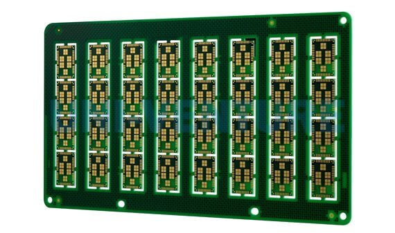
Fabrication needs the Gerber or another agreed-upon manufacturing data set; drill files, fabrication drawing, stack-up notes, and special instructions identifying items not explicitly defined via copper artwork. A fabrication drawing will document the dimensions, tolerances, material type, finish, drill file, and any other instructions which cannot be determined by viewing the copper artwork alone.
SUGA will ensure that the Gerber layers, drill data, and the fabrication drawing indicate the same version of the PCB before ordering fabrication. A mismatch between layer names or stale drill files could go undetected by a visual inspection, but could prevent the fabrication engineer from manufacturing the PCB.
Customer Drawing and Smart Manufacturing Outputs
Some customers may have requirements for formal drawings, whether in terms of formatting, naming conventions, etc. These requirements will be identified in the agreed-upon version number and approval documentation.
Gerber and drill files remain the most common outputs for fabrication. ODB++, IPC-2581, or Gerber X3 may be requested if a customer needs a more detailed representation of components, tooling, assembly or inspection data in an all-encompassing intelligent data set. These document types are quoted deliverables and are not automatic replacements for all current documents.
Version and Approval Notes
The final engineering document package will contain engineering questions, customer decision, a record of all documented file changes, and the status of final acceptance for the customer. For any open exceptions, there must be a visible action. This record will be used by the subsequent team to understand the risks that were resolved, accepted or excluded from the quoted work.
The document sets will be grouped according to their respective use:
- Design archive – editable source files, libraries, constraints and notes identified in the customer quotation
- Fabrication – the board data, drill files, fabrication drawings, stack-up notes, and version number
- Assembly – BOM, pick-and-place or centroid data, assembly drawings, polarity and process notes
- Customer drawing control – the agreed-upon format and approval identifier assigned to the customer
- Project record – engineering questions, decisions and final acceptance.
PCB Design Applications
The application specifications determine how PCB layout files will be set up. The application specifications include electrical, mechanical, thermal, reliability, and compliance, whereas the application label is primarily the business segment. Each application provides unique information about how to collect PCB layout files, set PCB design constraints, and how to review evidence before manufacturing the PCB.
Consumer Electronics
The Consumer Electronics business segment consists of small, portable devices that incorporate wireless, display, battery, charging, and user-interface circuits into a compact enclosure. The PCB outline, maximum height of the enclosure, accessibility of connectors, and layout areas for antenna are critical to PCB design. The review process for a consumer electronics PCB focuses on the stability of component footprints; the mechanical fit of the PCB into the enclosure; and the assembly data for the PCB that accurately match the final mechanical design.

Industrial Automation
The Industrial Automation segment consists of devices connecting all the components needed to sense, actuate, communicate, and supply power in an environment filled with electrical noise. Designers must gather all the design inputs needed to isolate circuits, define connectors, establish current paths, and provide test access. SUGA uses these inputs to define placement zones, routing rules, and other production data for design teams to identify by version.
Medical Electronics
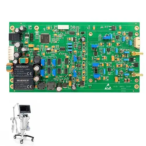
Medical Electronics devices must start with defined product requirements and the applicable regulatory path for compliance certification. While the customer's design responsibilities for a Medical Device include isolation, traceability, power, sensing, and enclosure design constraints; the Design Review will provide an organized and complete collection of the defined product requirements and the associated output records. Medical Devices are certified for compliance and quality-system certification by the certifying body; however, the customer retains ownership of the Medical Device requirements and certification path.
Automotive Electronics
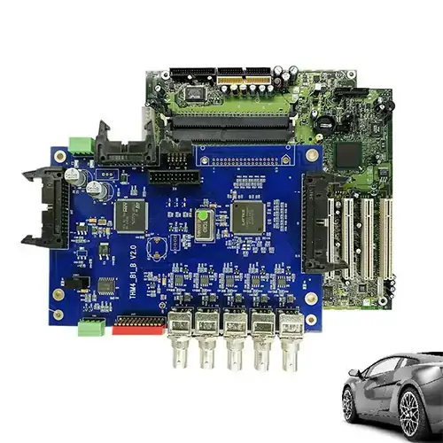
Automotive Electronics includes transients, temperature, vibration, force applied to connectors, and high-current routing, which may differ from other PCB layout options. The customer's applicable electrical, mechanical, and qualification information will be supplied to SUGA before using SUGA for the PCB design. SUGA evaluates the plan to map the protective needs, heat paths, and spacings of these components so that, during manufacture, the assumption of one vehicle environment for all systems is avoided.
IoT Devices
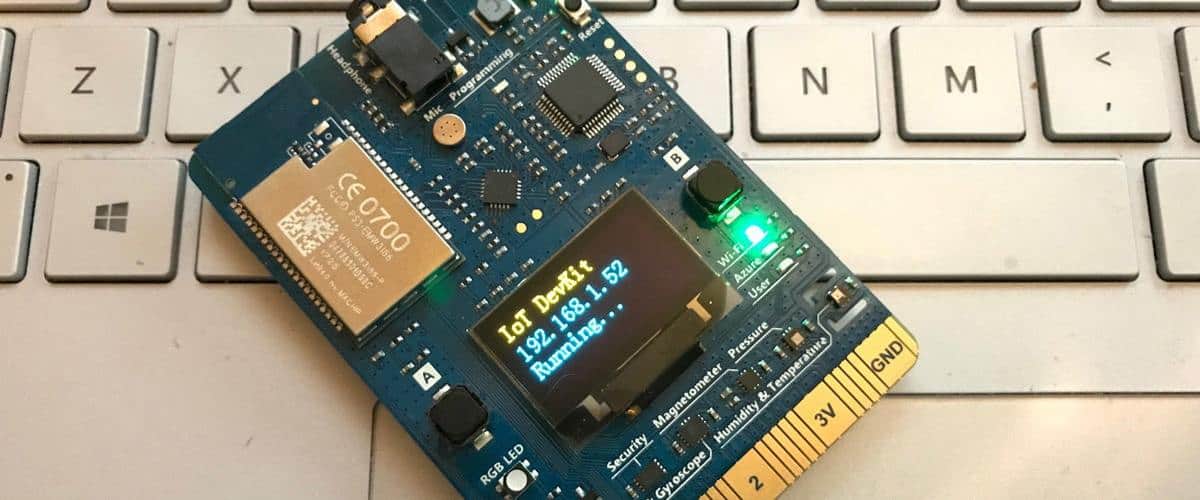
Several IoT devices involve a controller board that will contain RF modules, sensors, low-power controls, and other interfaces to interact with the cloud. The placement of antennas, power paths, idle currents, connector access, and enclosure material types interact and will be reviewed before making last-minute changes to either the RF antennas or batteries.
Data Communication
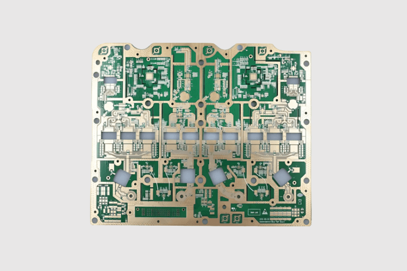
The type of board used to create a reliable data communications link depends upon the interface speed, topology of the circuit, connector style, reference plane, and acceptable loss levels. The specification of the input package must provide the serial standard, channel budget for the purposes of design validation, and how an input is verified to work. The layout review will control differential pairs, identify return-path transitions, validate power delivery, and provide stack-up assumptions to establish what the PCB manufacturer must produce.
Optical Network
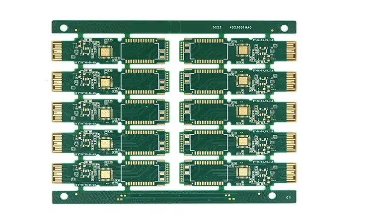
Optical network hardware places sensitive transceiver interfaces beside clocks, power conversion circuits, and high-speed digital circuits. Layout review is needed to determine what the layer, location, or placement of components is likely to be, what the limitations are to the trace lengths of each signal path to preserve SI, and the thermal paths from components.
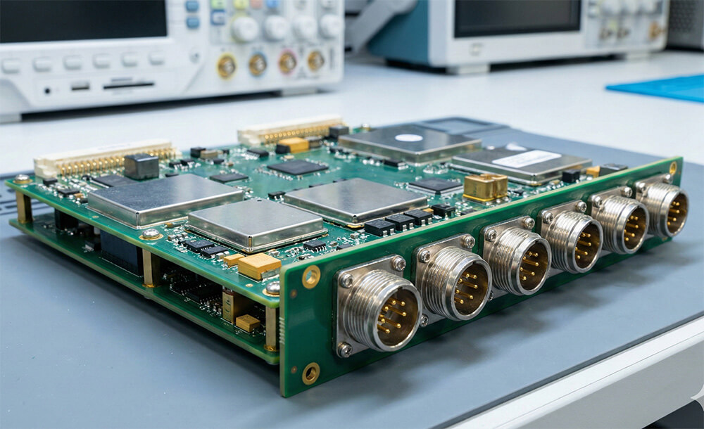
Aerospace and Defense
Working for either the aerospace or defense contracting industries requires controlled materials and documentation, strict traceability of purchased components, and qualification requirements. The actual contract defines the environment in which the product will be operated and authority or standards applied to those environments. SUGA is available to assist with design reviews and prepare material for manufacture while all other processes, documentation, and control methods will be determined at the program/contract level.
PCB Design Cost and Lead Time Factors
Factors affecting the total PCB design cost and lead time include complexity of routing, completeness of the submitted information, the type of technology used on the PCB, the level/number of analyses performed on the PCB and the desired end format of the physical PCB and number of changes after the initial release. The number of layers cannot determine PCB quote costs since the same PCB may have a different complexity depending on the timing of completing the package data, mechanical constraints, impedance specifications, or the timing of any required approvals during the design process.
The terminal pin counts below are based on the terminal count defined in the capability table and must be confirmed by SUGA before establishing a delivery timetable. This is necessary for each schedule to correctly reflect the workload required by the routing activity.
| Pins per single board (terminal count) | Layout period (working days) | Conditions to state | Missing-input risk | Rush condition | Best next action |
|---|---|---|---|---|---|
| Less than 1000 | 3–5 days | Stable schematic, footprints and ordinary constraints | Rework if connectivity or board outline changes | Possible with frozen requirements | Submit the current file set for review |
| 2000–3000 | 5–7 days | Defined package data and placement constraints | Placement churn can delay routing | Possible with limited change rounds | Confirm BOM and mechanical inputs |
| 4000–5000 | 8–12 days | Stack-up and major interfaces identified | Unknown rules can reopen layer planning | Case-by-case after constraint freeze | Request constraint review before routing |
| 6000–7000 | 12–15 days | High-density interfaces and power needs documented | Incomplete constraints expand review cycles | Limited; depends on interface clarity | Supply interface and power requirements |
| 8000–9000 | 15–18 days | Critical nets and package escape strategy defined | BGA/via changes can alter board technology | Limited; package data must be final | Confirm package and via assumptions |
| 10000–13000 | 18–20 days | Large netlist and input set frozen | Version mismatch creates repeated checks | Not recommended without frozen inputs | Freeze and label the input set |
| 14000–15000 | 20–22 days | Review depth and deliverables agreed | Added analysis or formats can extend work | Not recommended | Agree outputs and analysis before quote |
| 16000–20000 | 22–30 days | Complex technology and confirmation cadence planned | Late changes create significant rerouting | Not recommended | Use milestone approvals and change control |
The periods are meaningful only with their conditions; therefore, while a small terminal count may appear insignificant in nature, many other circuit applications exist behind a small terminal count (i.e. RF, rigid-flex, high voltage, mechanical work). For example, a larger board that uses established libraries, cleared constraints, etc., is generally easier to manage and plan than a smaller board for which its package and outline may change during routing.
Complexity Drivers
Routing needs will generally be based on pin counts; pin counts alone generally do not determine the areas of the board where the most routing activities will occur. Package escape rules and interfaces are usually important to determining where the majority of routing activity takes place. The use of fine-pitch BGA packages, HDI, rigid-flex, RF, high-power or mixed-technology boards generally add additional planning and checking processes. Using conversion tools, having an incomplete footprint library and producing formal drawings can create a significant amount of added workload, even for a board whose copper geometries are standard.
The quote illustrates how each complexity driver connects to an action. For example, when a board uses a dense BGA configuration, the designer may need to provide a fan-out plan and confirmation of the ability to manufacture the specified board. Similarly, a designer working with high-speed circuits may need to include stack-up, loss values or validation inputs before routing may continue. A board that uses a rigid-flex design may require mechanical and bend information; therefore, a designer must either include this information in the initial package or provide it in a note or separate documentation.
Lead Time Variables
Lead time begins to accumulate from the time an appropriate set of design inputs is ready for the work quoted above. If the schematic, BOM or board outline changes after the routing process has begun, then the estimated lead time must include time to re-plan the work, time to inspect any affected routing, and time to re-inspect after the work has been completed. A customer's response time also has a direct impact on the planning process, as lack of resolution on an open issue may prevent the completion of dependent tasks.
Examples such as 1 day, 24 hours, or 5 days, are generally used to identify the manufacture or turnkey phases of the quoted process. For example, 24-hour or 48-hour quotes may be used with fast review or quote turnaround times. Neither statement is a guarantee to complete the development, evaluation and release of a complex PCB within that timeframe.
Pricing Inputs
A PCB design quote may be offered as either an hourly or project-based price. An actual quote would depend on board technologies chosen, the amount of completeness of source files, the level of depth in engineering review, the types of final deliverables required, and who is in charge of processing and coordinating the fabrication or assembly of your PCB.
Procurement should ask what is included in the price: Electrical review, layout, library work, DFM/DFA, SI/PI, drawings, Intelligent Manufacturing Data, and Change Rounds can all be independent components of the overall PCB design quote.
PCB Design Support and Next Step
Next steps will be influenced by the status of your PCB files and any decisions that require guidance from engineers. If your design files are complete, they may qualify for the first stage of review; however, if there are areas that require engineering input, then you need to contact an engineer for clarification. When it comes to PCBs of high-speed, HDI, RF, Rigid-Flex, and Dense BGA types, it is important to discuss constraints first, and if your project has final production data, you must send the data for fabrication or assembly review.
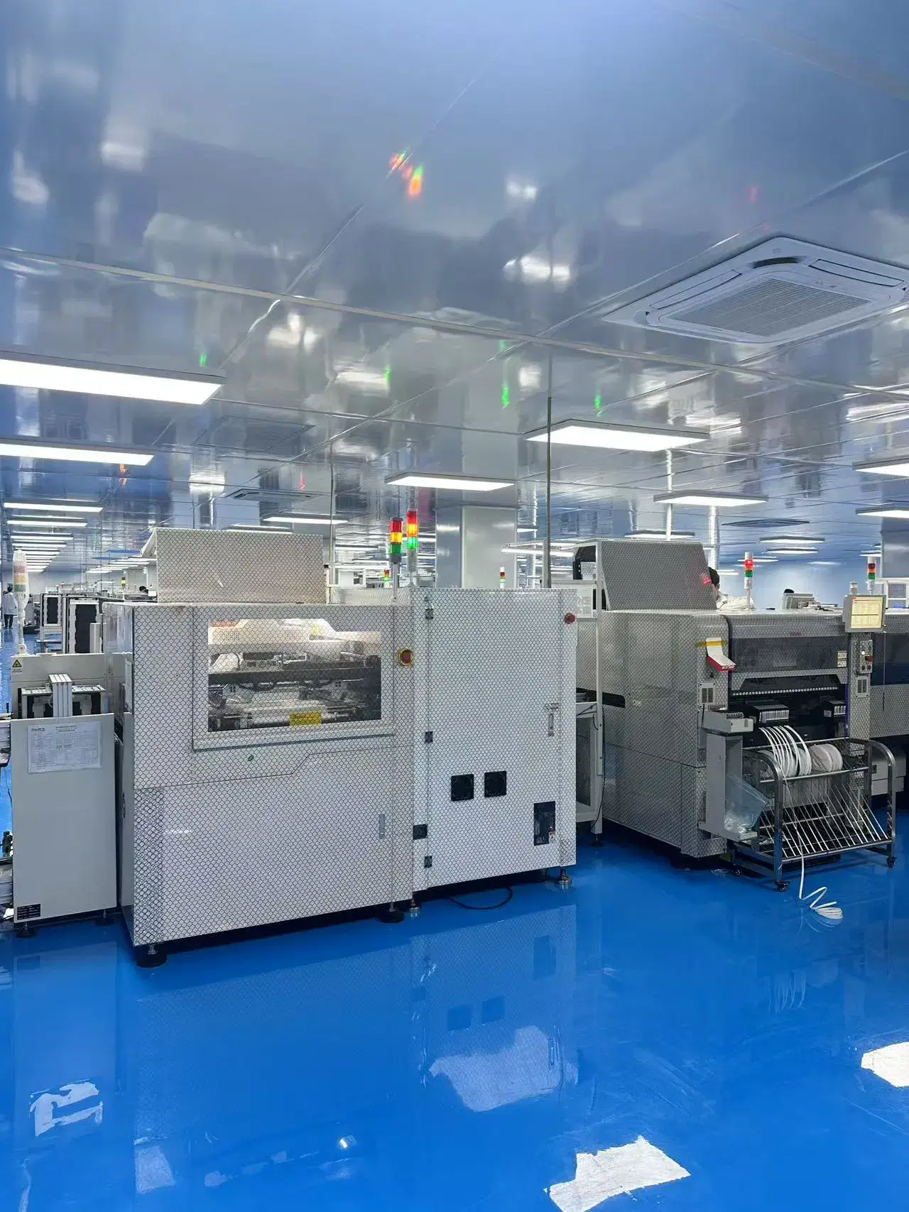
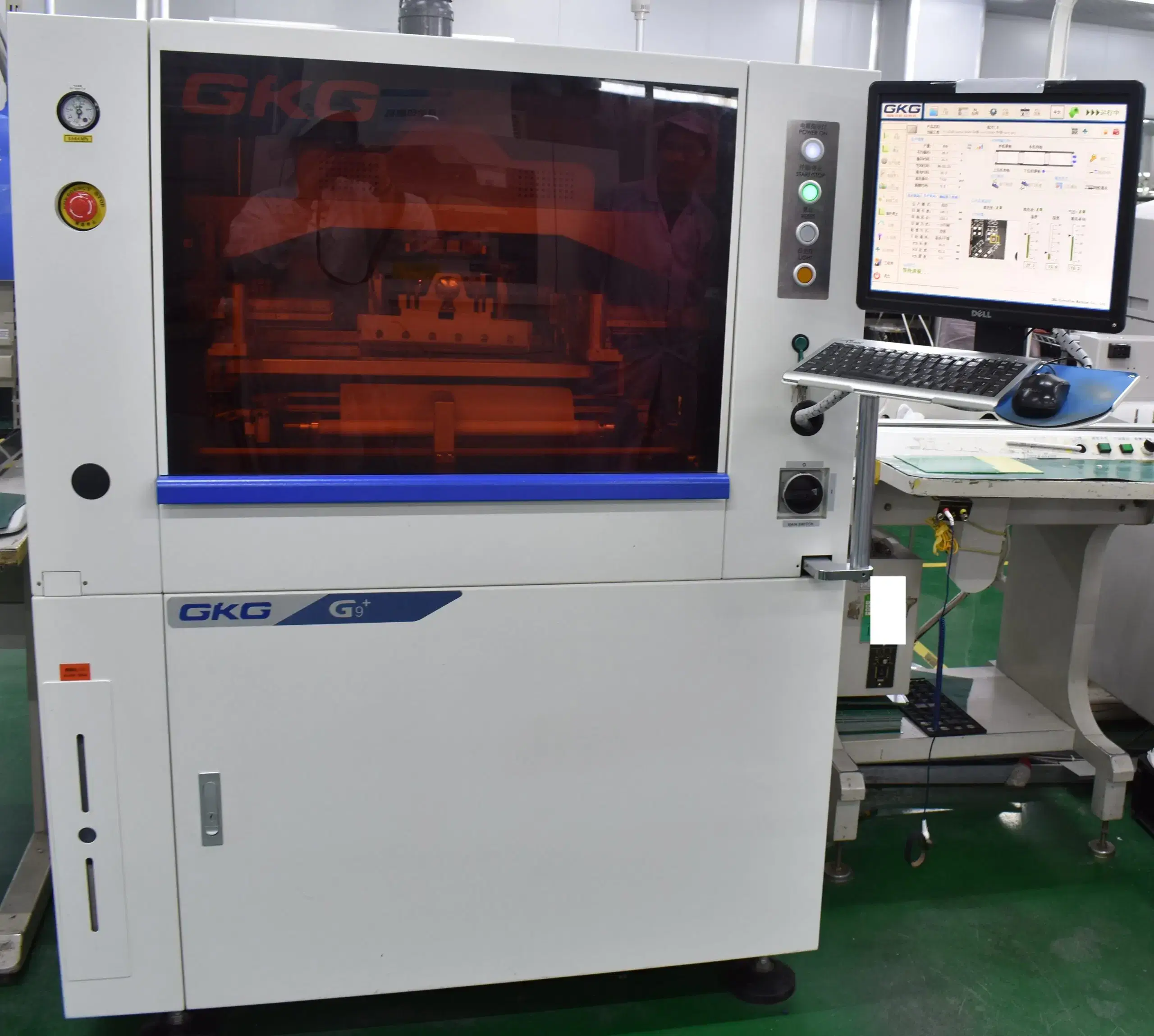
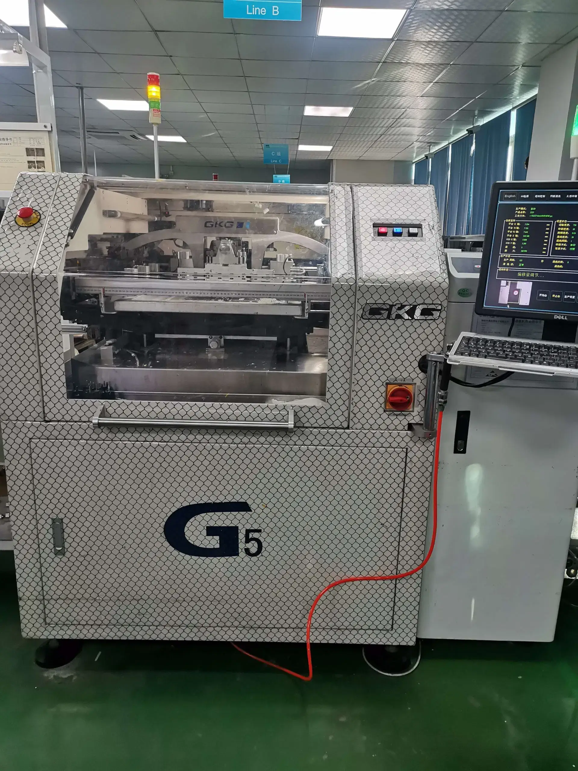
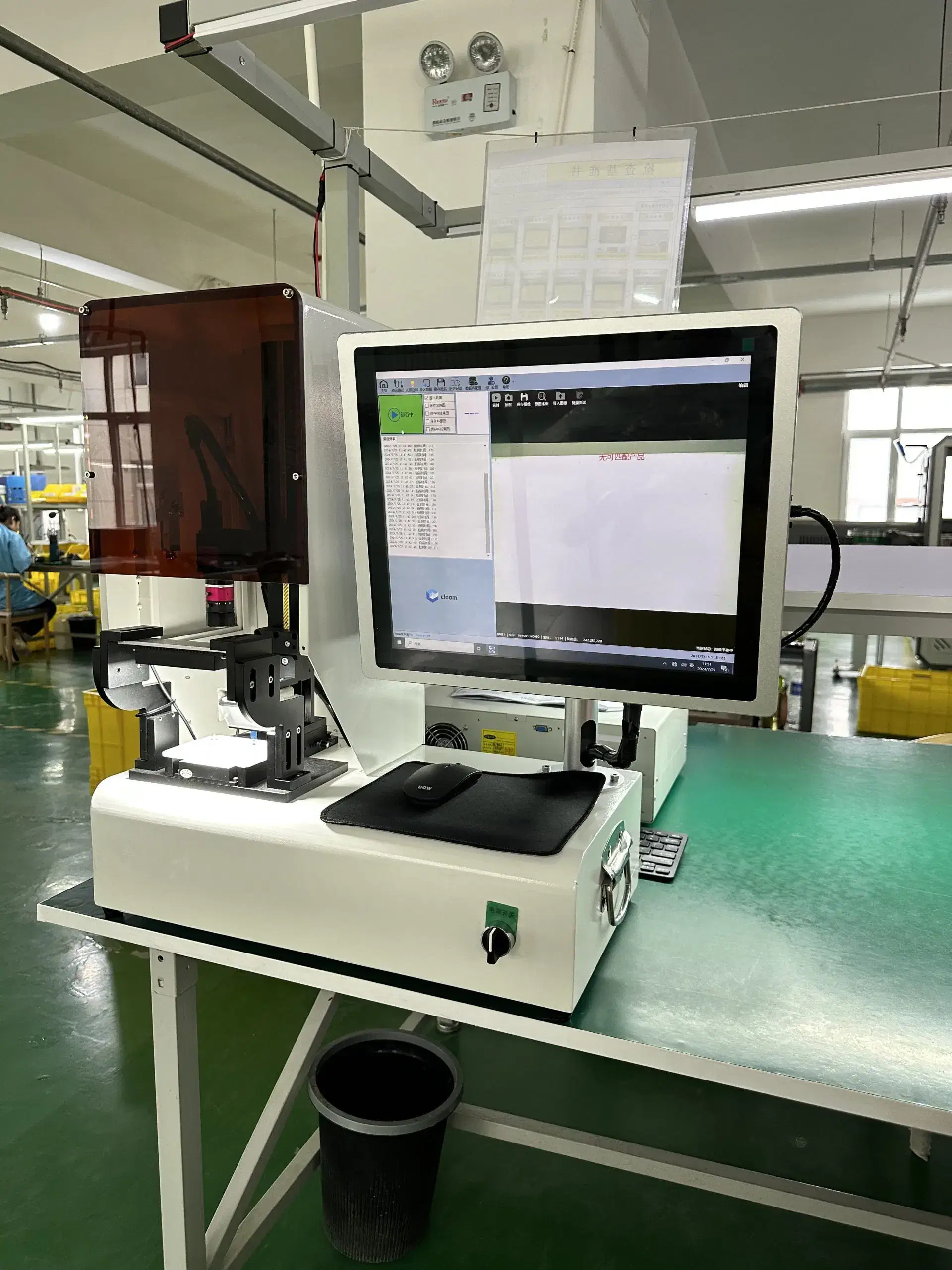
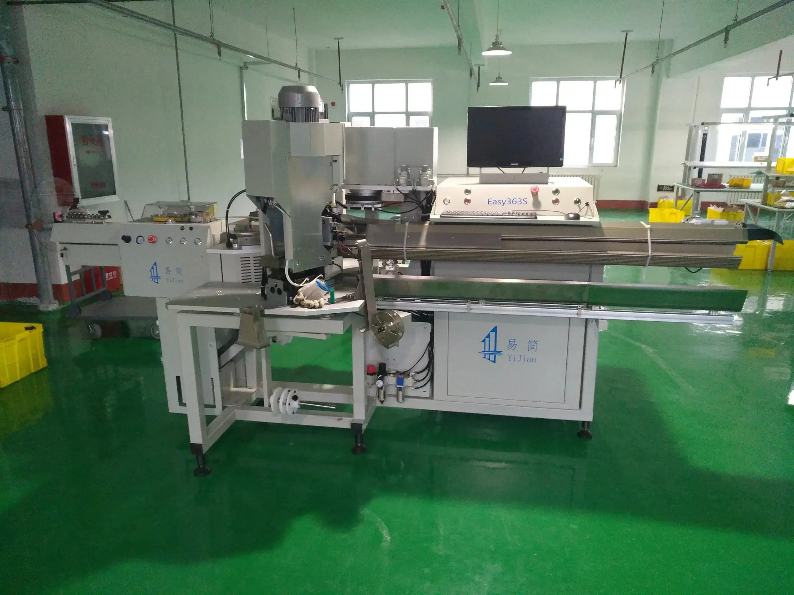
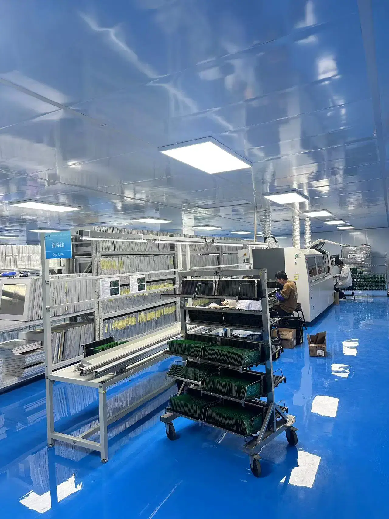
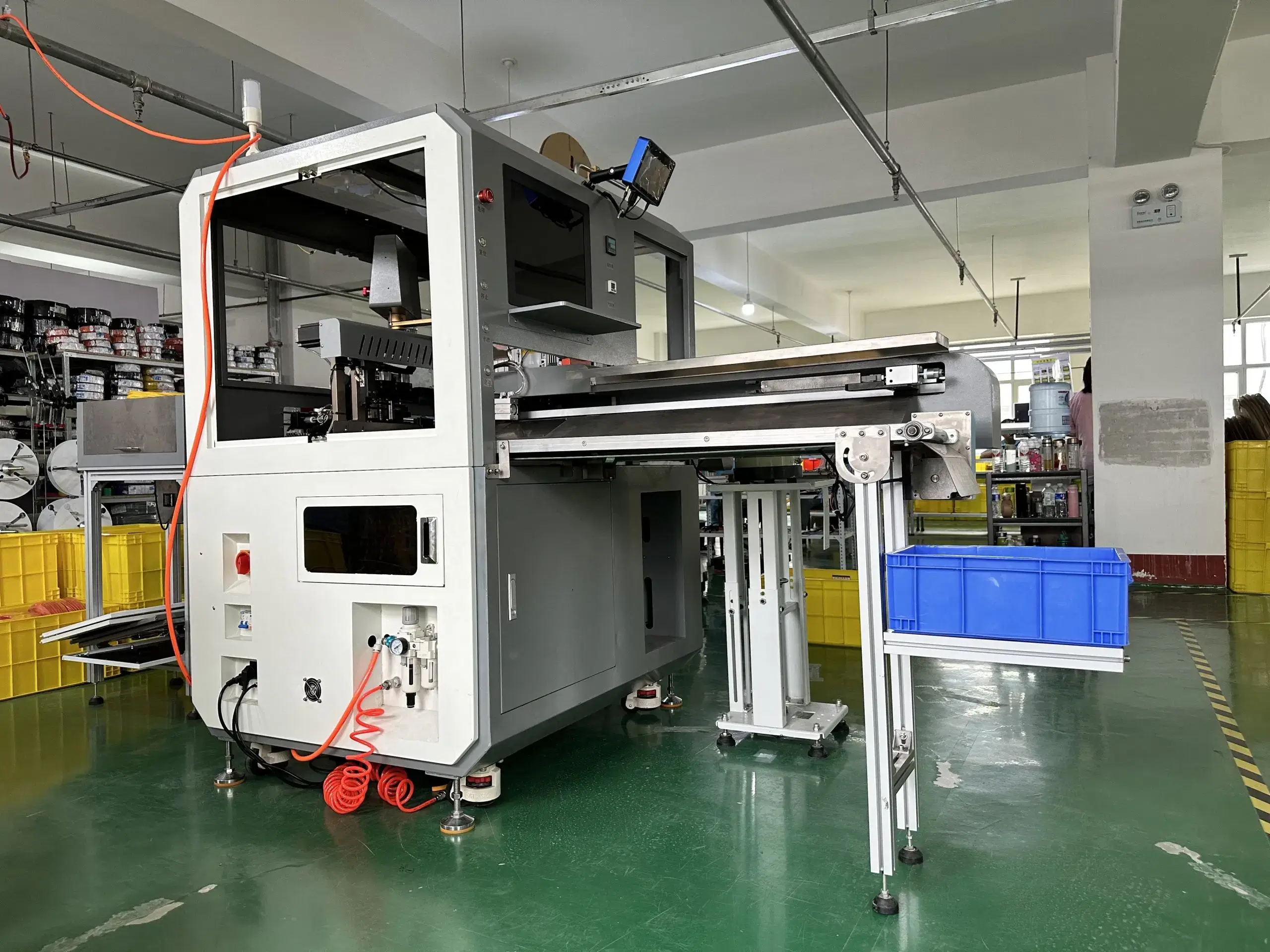
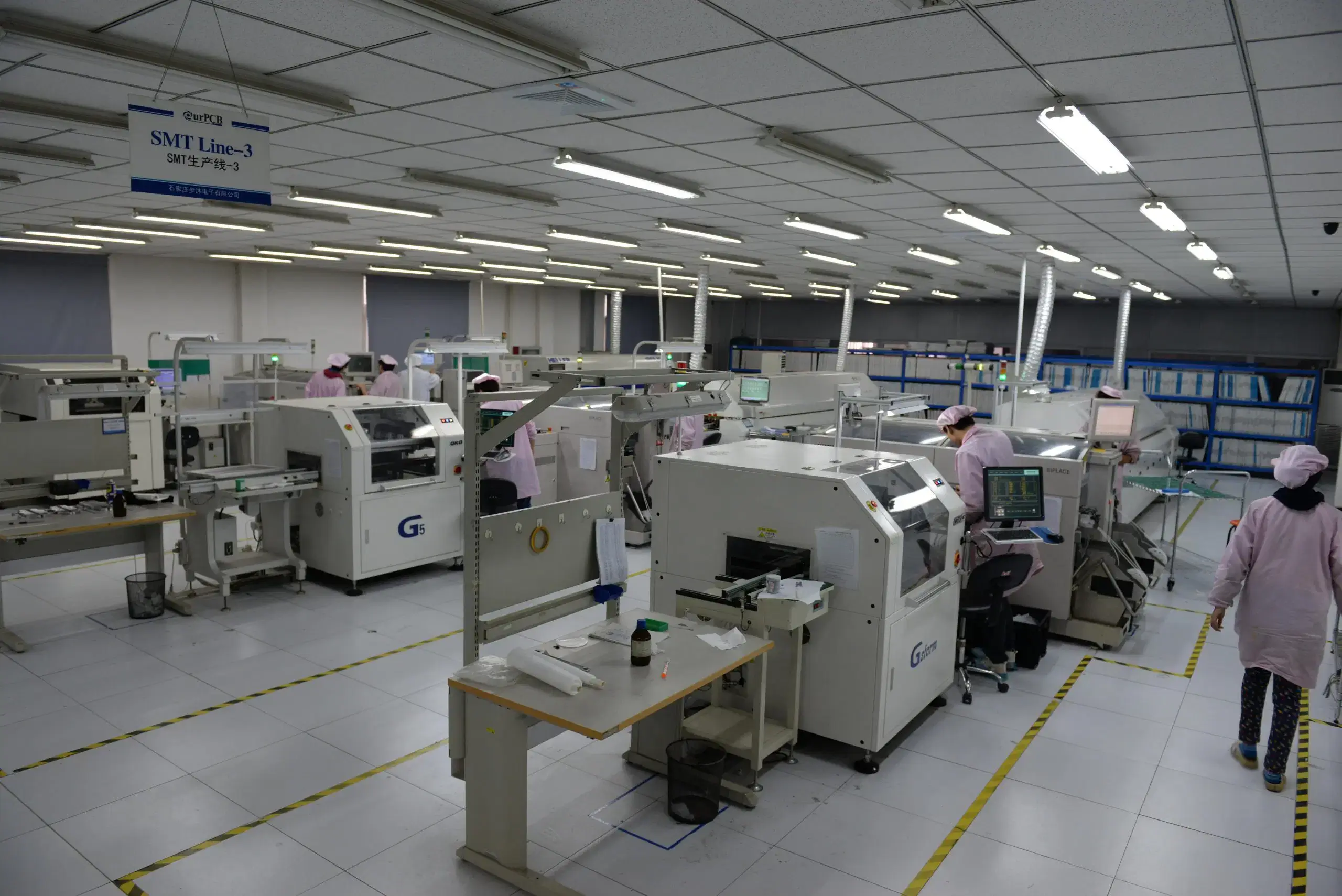
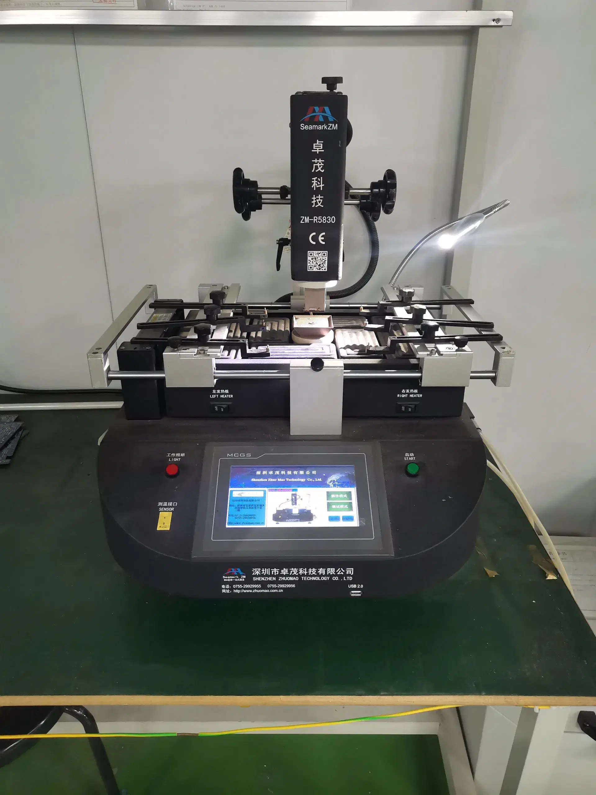
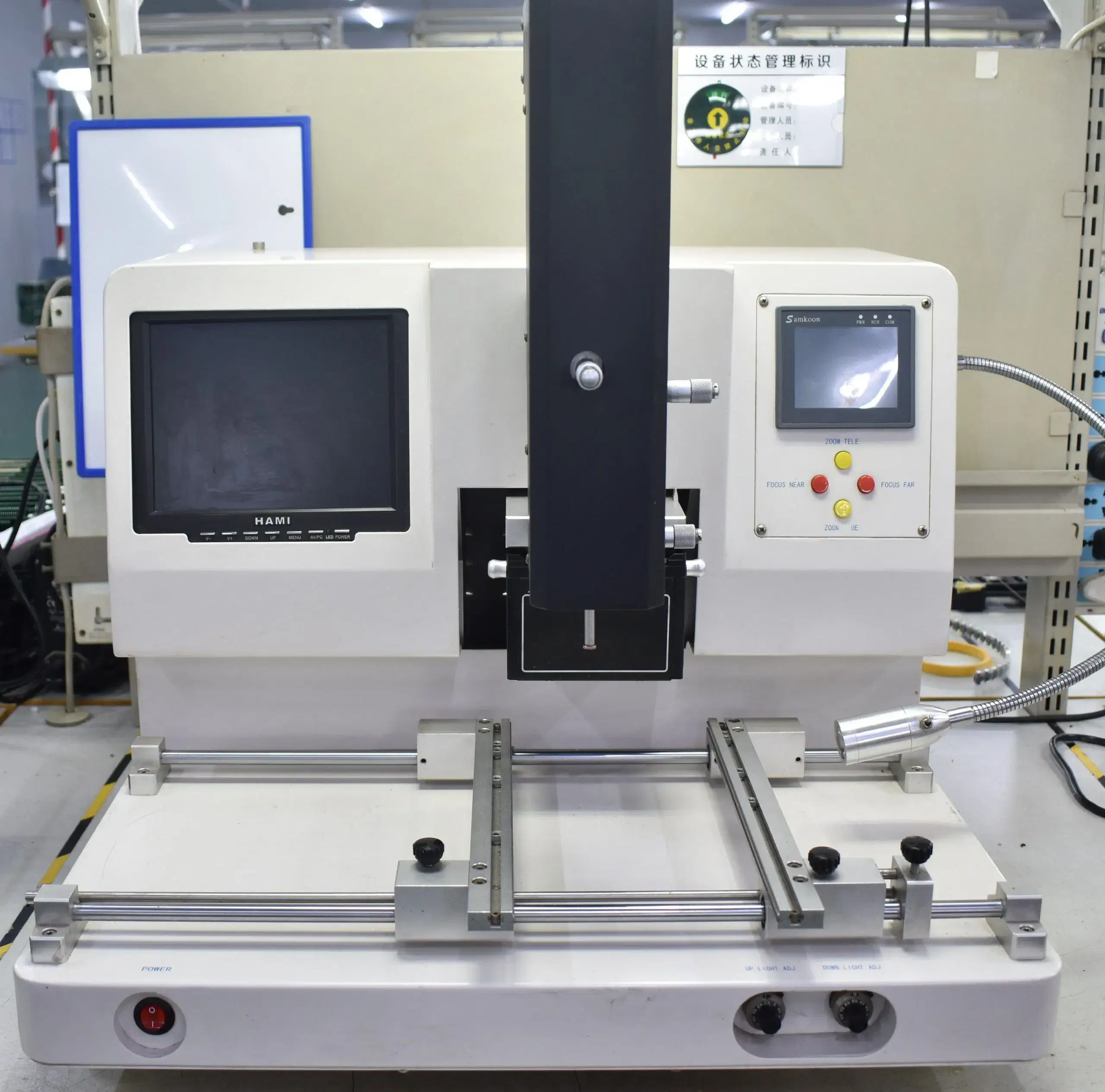
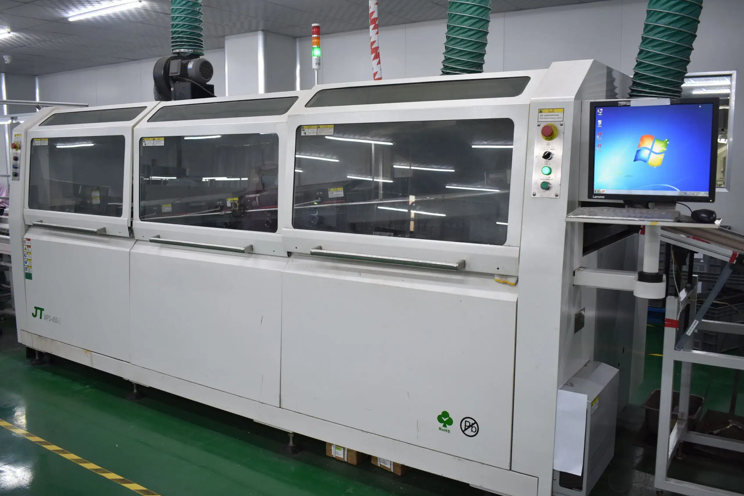
Our PCB Factory Gallery



FAQ
Yes. Using the original design, the available source files, Gerber data, BOM, drawings, photographs, measurements, and functional specifications, SUGA will review your documents and define whether it can support redesign, layout reconstruction, or manufacturing review based on the available evidence. To assist the redesign process, SUGA evaluates the design specifications to separate verified information from assumptions before starting to create the PCB design.
Understand the differences between PCB design companies in their definition of input files, engineering responsibility, layout constraints, DFM/DFA reviews, deliverables, and agreement for change approval. For PCB Projects that require the use of High-Speed Technology, BGA Technology, RF Technology, HDI Technology, or Rigid-Flex Technology, inquire about how a particular supplier can confirm the stack-up method, package data, and fabrication limits before proceeding with PCB Production.
Yes, one supplier may coordinate PCB design, fabrication and assembly provided each process has a clear definition of the work and a defined approval point. The final PCB Design Package would identify the accepted design version, fabrication outputs, and assembly output. Any open items still requiring review would also be identified.
Yes, SUGA will sign a mutual NDA before obtaining any schematics, BOMs, or source files. Additional information on residual rights, sub-supplier disclosure, and retention of the data can be agreed in advance.
Yes; however, this would need to be listed as part of the quote. The quote provides a deliverable list that details the source files (e.g., native Allegro, Altium or PADS source files), the library used, and any associated project constraints. It will clarify if only manufacturing data will be provided.
Quotes state the number of change rounds included in the pricing, and the amount charged for additional changes. Engineering Change Orders will be created when a schematic, BOM or outline has been modified after inputs are frozen; supplier-side rework remains in the original quote.