Upload BOM & Gerber
-
Mobile: +86 13312967631
-
Email: sales@sugaintl.com

Rigid-Flex PCB and FPC Manufacturer in China
Rigid-Flex PCB and Flexible Printed Circuit Manufacturing Services
SUGA can assist customers in ordering FPCs and rigid-flex PCBs by providing the necessary materials and stackup definitions and then moving on to bare-board manufacturing, SMT assembly, visual inspection, and electrical testing before the boards are used in final product assemblies. Rigid zones, flex zones, bend duty cycle, copper structure, via design, component support, and testing requirements define rigid-flex PCB and FPC construction.
40-layer
Rigid-flex
2/2 mil
FPC trace / space
3,000 mm
Extra-long FPC
What Are Rigid-Flex PCBs and Flexible Circuits?
FPCs are etched flexible circuits built on a thin dielectric layer, such as polyester or polyimide, and are used to carry electrical signals or power through bends, folds, movement, or limited spaces. Rigid-flex PCBs incorporate rigid sections and flexible interconnects, all of which are laminated together to form one structure. Rigid-flex printed circuit boards have flexible layers running through the rigid-to-flex transitions; therefore, the layers do not terminate at separate cable connectors.
| Selection criterion | Rigid PCB | FPC | Rigid-Flex PCB | FFC |
|---|---|---|---|---|
| Construction | Rigid laminate | Etched flexible circuit | Integrated rigid/flex laminate | Parallel-conductor flat cable |
| Structural support | Full-board support | Local stiffener at terminals or component areas | Rigid zones with engineered flex sections | Connector- and installation-dependent |
| Flex duty | No designed bending | Static, flex-to-install, occasional, or dynamic | Controlled bends between rigid zones | Routing or folding per cable construction |
| Component assembly | Supported rigid surfaces | Supported or stiffened local areas | Primarily rigid zones | Not component-bearing |
| Interconnect model | Cable or connector between boards | Connector or solder termination | Continuous interconnect across rigid zones | Compatible connector required |
| Primary use case | Non-flexing electronics | Thin or moving custom interconnect | 3D assemblies with multiple component zones | Replaceable standard cable |
Because rigid-flex PCBs and FPCs are fundamentally different, the choice between an FPC and a rigid-flex PCB typically depends on integration, mechanical duty cycle, and ease of maintenance. FPCs minimize interconnect thickness, while rigid-flex PCBs eliminate selected board-to-cable connectors and the associated connector failures. A rigid board with a removable cable may be preferable when field repair, modular cable replacement, or lower bare-board complexity is more critical than connector elimination.
FFC and FPC are not interchangeable terms. FFC refers to a finished cable configuration with parallel conductors and a standardized pitch. FPCs are custom printed circuits, with traces, pads, branches, openings, shielding, and reinforcement designed to meet the electrical and mechanical requirements of the intended application.
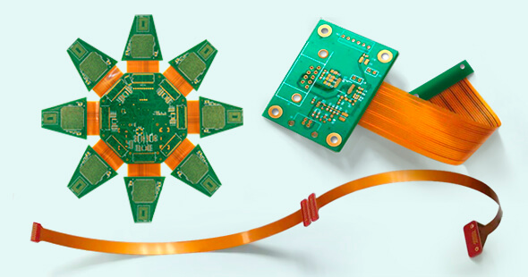
Which Flex Structure Fits the Product?
The lightest viable construction will meet routing density, mechanical duty, impedance, current, length, and assembly support requirements. Though it may be possible to add additional layers to resolve routing issues, additional copper or dielectric layers will also increase the rigidity of the part, make registration more difficult, and increase thermal load and bend stress.
FPC Layer Structures
Single-sided flex circuits are typically used for sensors, switches, jumpers, and other simple interconnects that are installed in a static position or used where the bend is controlled. Thin-material handling, coverlay registration, and reinforcement of the terminations protect the one-layer structure. Double-sided flex circuits provide plated-through connections for routing on two sides. For static or infrequent flexing, via reliability, copper balance, and plated-hole keepout help protect the connections. Multilayer flex circuits enable denser routing, shielding, and controlled impedance with a maximum of 12 layers. Layer registration, adhesive flow during manufacturing, finished flex thickness, and neutral-axis control are matched to flex-to-install or limited-movement requirements.
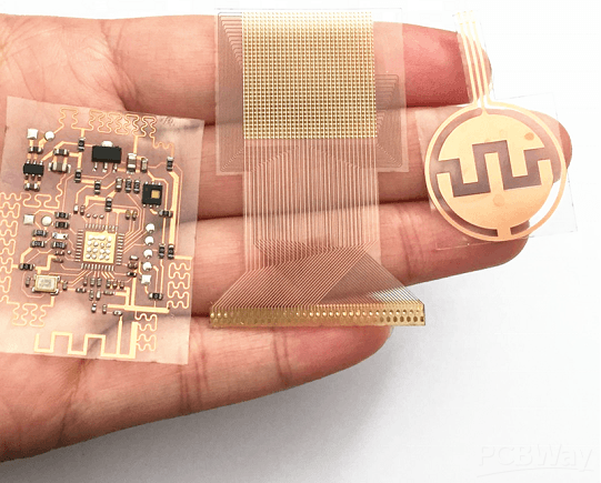
Dynamic Rigid-Flex
Dynamic rigid-flex designs can be applied to assemblies that must move repeatedly while maintaining stable rigid component zones. The stackup selection will vary according to the required radius, angle, speed, temperature, and number of cycles required by the end-use application. The use of RA copper, balanced flexible construction, smooth trace geometry, extended transition lengths, and cycle validation will support repeated movement. A lighter construction and validation program will be required for flex-to-install circuits than for dynamic-motion designs.
Extra-Long FPC
Extra-long flex circuits are generally used in battery sensing, scanners, imaging equipment, lighting, and other applications that require extended conductor paths. The use of shrinkage compensation, long-format registration, stable datums, protected handling, profile tolerances matched to length, and end-to-end electrical testing will help control the full conductor path.
Bookbinder Rigid-Flex
The bookbinder configuration of rigid-flex designs supports multiple folds or several distinct rigid-zone groups through the use of unequal lengths within the flex layers. Multi-flex assemblies use independent segments between rigid zones. The drawings must include layer-length compensation, transition geometry, fold sequence, bend direction, and relationships between rigid zones.
FPC Materials and Stackup Construction
The first decision regarding material selection for a flex section must be whether the section will only be bent during assembly or will flex throughout its life cycle. This distinction directly drives the selection of copper foil, adhesive systems, finished thicknesses, bend radii, shielding construction, and validation programs. Once the assembly temperature, dimensional control, current ratings, impedance, and reliability requirements have been established, the range of potential stackups can then be limited.
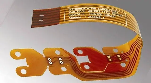
| Laminate system | Motion class | Process impact | Engineering limit |
|---|---|---|---|
| Polyester (PET) | Static / low-cycle | Thin, cost-efficient construction | Lower reflow and cycle margin than PI systems |
| Adhesive polyimide | Static / flex-to-install / occasional | Adhesive affects thickness, moisture, flow, and dimensional control | Less suited to ultra-thin or dynamic stacks |
| Adhesiveless polyimide | Fine-line / dynamic / impedance / high-reliability | Thinner construction with stronger dimensional stability | Higher material cost and tighter processing |
Flex Material Construction
RA copper is the preferred conductor material for flexible conductors that will see repeated bending, as it has a grain structure that better adapts to deformation in these applications. Electrodeposited copper is generally used where stackup criteria such as rigid-zone processing, available foil constructions, feature definition, or price are driving factors. The ability of a copper conductor to carry current is primarily governed by the copper cross-section and surrounding thermal environment. A representative flex core is constructed with 0.5 oz RA copper on a polyimide core of 0.05 to 0.1 mm; the final stackup establishes the strain and thickness of the final assembly.
Using heavier copper increases both the current capacity of the conductor and the flex stiffness. Current capacity and bend life are determined based on the conductor width, copper thickness, coverlay thickness, expected temperature rise in the conductor, and the motion profile associated with use.
Coverlay protects flexible conductors and defines pad openings. Flexible solder mask can provide more localized opening definition within specific assembly areas. Each serves a unique set of requirements based on the zones of the finished assembly, while coverlay registration, adhesive flow, and transition overlap all affect fabrication and assembly.
A stiffener increases localized strength. PI, FR-4, PET, stainless steel, or other engineered materials can establish connector thickness, support soldered components, resist insertion forces, distribute strain, or create a mounting point. Conductive film, copper, or a dedicated shielding layer can provide EMI shielding and is incorporated into the overall thickness, grounding, and bend-stiffness calculations.
Rigid-Flex Zone Architecture
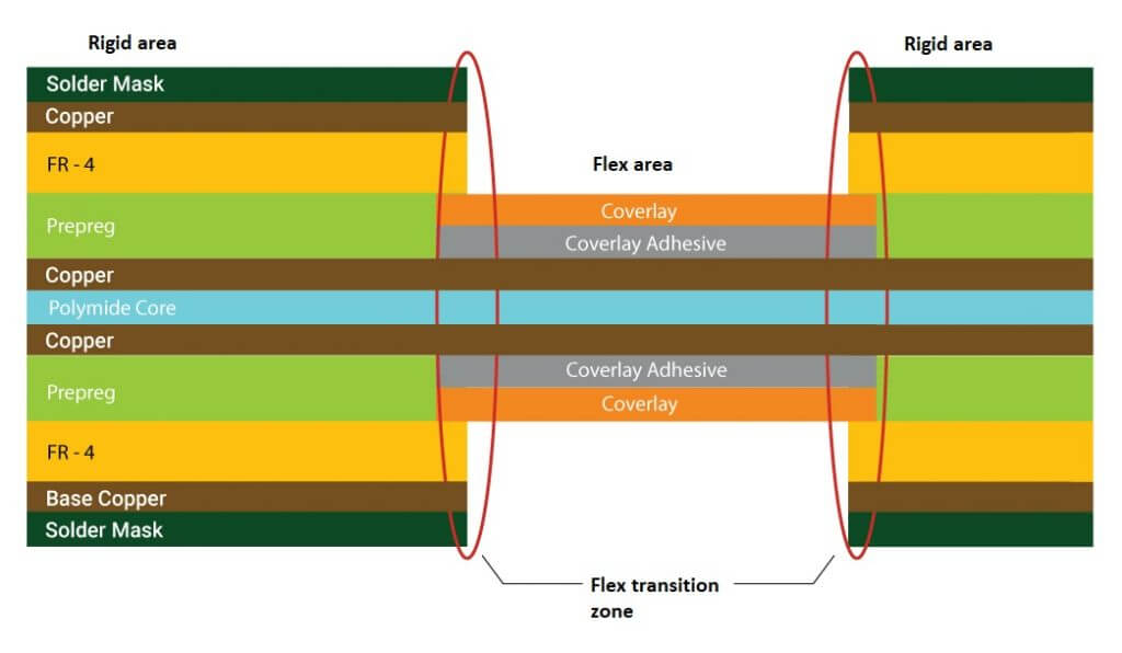
In a typical rigid-flex construction, the flex core extends through the rigid-to-flex transition, while the rigid dielectric layers and rigid-only copper layers terminate before reaching the exposed flex window. The termination point for each layer will vary based on many factors, including the stackup architecture, impedance structure, via system used, and required bend duty.
| Stackup feature | Zone assignment | Functional role | Process control |
|---|---|---|---|
| Rigid outer copper | Rigid zone | Component pads, routing, planes | Copper weight vs. current and feature density |
| Rigid dielectric | Rigid zone | Structural support and dielectric spacing | Rigid-zone thickness and impedance |
| Shared RA copper | Rigid + flex | Signal or reference continuity | Copper balance and bend geometry |
| Polyimide flex core | Rigid + flex | Flexible dielectric and flex backbone | Motion class, thickness, impedance, thermal duty |
| Coverlay | Flex zone | Conductor protection and pad openings | Opening registration, adhesive flow, transition overlap |
| Stiffener | Local flex area | Connector or component support | Thickness, insertion load, thermal demand |
| Shielding | Selected zones | EMI control | Ground path, added thickness, bend stiffness |
Bend Zones in Rigid-Flex Manufacturing
The design of the bend is critical to manufacturing feasibility. The flex thickness, number of copper layers, copper type, plane geometry, and transition-area design will dictate where the maximum strain will accumulate. The drawing layout includes the bend axis and direction, bend angle, radius, motion class, and location of the active bend area.
| Flex condition | Preliminary DFM radius | Key DFM controls |
|---|---|---|
| Single-layer FPC | 3–6× finished flex thickness | Smooth traces; no vias in active bend |
| Double-layer FPC | 7–10× finished flex thickness | Balanced copper; plated-hole keepout; controlled transition |
| Multilayer FPC | 10–15× finished flex thickness | Layer symmetry; plane control; wider keepouts |
| Flex-to-install, 1–2 copper layers | Start near 10× thickness | Fixed installed bend; avoid repeated reforming |
| Four-layer flex section | Start near 20× thickness | Increase radius for added copper, shielding, or adhesive |
| Dynamic movement | Angle, speed, temperature, cycle target | Thin balanced stack; long transition; cycle validation |
These radius ranges are defined based on DFM criteria and are not necessarily universal acceptance limits. They will be verified using multiple factors, including the finished flex thickness, copper type and grain direction, bend angle, travel path, torsion, temperature, speed, and target cycle count. The installed bend should always remain within the defined active flex zone.
Conductors should meet the bend axis at right angles, while curved routing, gradual width changes, staggered traces, and evenly distributed copper reduce the potential for stress concentration compared with sharp corners, neck-downs, or stacked conductors.
Using a solid reference plane to support the signal return will increase the stiffness of the bend by providing a stable return path.
Hatched copper reduces stiffness while changing impedance and return-current behavior. Keep vias, plated holes, component pads, stiffener edges, and abrupt plane changes outside the active bend and rigid-flex transition. Teardrops, fillets, tapered copper, and controlled coverlay overlap assist in developing a gradual stiffness change during the rigid-flex transition while maintaining the transition’s integrity. Bonding materials and rigid-window geometries keep resin and unsupported edges outside the bend path.
The drawing will define where the coverlay, shielding, adhesive backing, and stiffeners start and stop. Changing these boundaries will change the location of the neutral axis and local stiffness. For repeated motion, conductor width changes and plane openings need to be assessed throughout the entire travel path. Establishing a bend location with sufficient free length and mechanical strain relief is essential for keeping installation forces away from the rigid transition.
Rigid-Flex Fabrication and Assembly
Rigid-flex fabrication and assembly establishes a relationship between flex-window registration, transition stiffness, panel flatness, and local component support to determine whether the finished assembly remains stable during printing, placement, reflow, and handling.
| Operation | Critical process controls | Primary defect risk |
|---|---|---|
| Flex-core imaging | Film support; imaging; etch uniformity; copper balance | Distortion; over-etch; trace loss; misregistration |
| Coverlay preparation | Opening registration; cleaning; adhesive-flow control | Covered pads; exposed conductors; contamination; edge lift |
| Rigid-layer preparation | Rigid imaging; flex-window definition; low-flow bond setup | Window error; resin intrusion; layer mismatch |
| Layup / lamination | Tooling alignment; pressure; temperature; transition geometry | Layer shift; delamination; flex-window stiffening |
| Drilling / plating | Mechanical or laser drilling; desmear; plating; outer imaging | Hole breakout; weak PTH; outer-layer shift; flex damage |
| Routing / forming | Profile control; flex release; protected handling | Cut conductors; rough edges; creases; transition damage |
| Assembly preparation | Conditioning; carriers; stable datums; local support | Warpage; paste misregistration; workpiece movement |
| SMT / reflow | Supported printing; controlled placement force; mixed-mass profile | Paste defects; component shift; delamination; overheating |
| Post-reflow handling | Controlled cooling; carrier release; transport; storage | Cracked joints; point load; coverlay lift; contamination |
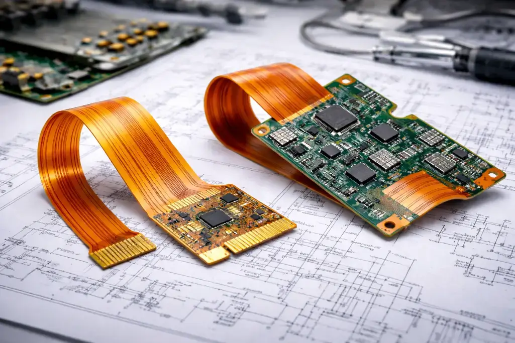
Flex Layer Lamination
During flex-core imaging, coverlay lamination, and subsequent rigid-flex press cycles, maintaining dimensional integrity through the flex layer is critical. A shared datum strategy is used to establish alignment of etched copper, coverlay openings, flex windows, and shared layers after repeated exposure to heat and pressure.
Preparation for rigid cores, flex windows, and bonding materials must take place concurrently. The bonding material used at the window edge protects the active flex area from resin intrusion because of its low-flow characteristics. Tooling must align all shared flex layers, rigid layers, and bonding materials before the pressure and temperature cycle creates one laminated rigid-flex panel.
Rigid-Flex Panel Formation
Laser-via sizes, pad diameters, drilling tolerances, and plated-hole aspect ratios must be examined together as a combined structure rather than separately. A design approaching the minimum hole or pad value may require fewer layers, a thinner finished construction, wider registration allowances, or a different via geometry than a design approaching the maximum thickness or aspect ratio.
The method of providing support changes once a flexible section is released because the unsupported segment can crease or load the transition.
Carrier Support During FPC Assembly
FPC assembly begins when the finished circuit is secured on a carrier. The carrier provides stable datum location, keeps the circuit flat, supports various component areas, and prevents forces from concentrating on the active bend and rigid-flex transition.
When paste is printed, support is provided beneath the flexible circuit. This ensures that the stencil apertures remain registered as the paste releases. Controlled placement force limits flex-circuit deflection or movement at reinforced component areas. Large connectors, BGA packages, heavy components, and mechanically loaded devices are placed on rigid or properly reinforced zones.
Reflow Profile and Post-Assembly Handling
The reflow profile for the assembly must account for the rigid laminate, thin PI, copper, adhesive, coverlay, stiffeners, and component masses. The placement of thermocouples and the design of the carriers will facilitate the collection of the mixed thermal response associated with the assembly. Controlled heating will minimise the likelihood of delamination or coverlay lift, as well as underheated or locally overheated solder joints. Any THT or hand-soldered secondary operations will require bounded heat input near the flex structure.
Until the assembly has cooled, the carrier support will remain in place, and handling loads will transfer through the supported areas rather than the free flex section. The entire assembly will be inspected for creases, transition damage, contamination, coverlay lift, and mechanically loaded solder joints prior to shipment.
For a double-sided assembly, the use of the carrier and the processing sequence will provide support for first-side components while printing, placing, and reflowing the second side. The presence of local stiffeners, connectors, and heavy parts creates thermal-mass differences across the workpiece; therefore, profile measurements must be based on representative points located in the rigid and flex-adjacent areas. Selective soldering, hand soldering, press-fit insertion, and cable attachment require fixtures that transfer force through supported areas rather than the released flex tail.
Inspection for Flex Assemblies
| Defect mode / requirement | Verification method | Recorded result |
|---|---|---|
| Open / short / net mismatch | Fixture or flying-probe electrical test | Continuity and isolation result |
| Low-resistance path | Four-wire measurement | Resistance value against defined limit |
| Trace / coverlay / registration | Bare-board AOI + visual inspection | Image and dimensional record |
| Placement / visible solder | Assembly AOI | Presence, polarity, offset, visible-joint result |
| BGA / QFN / bottom-terminated joints | X-ray | Alignment, bridge, solder-distribution image |
| PTH / internal construction | Microsection or coupon | Hole-wall copper, registration, dielectric/resin record |
| Flex window / transition | Visual + dimensional inspection | Cut, crease, edge, coverlay, dimension result |
| Static / dynamic bend life | Product-profile bend test | Cycle count and resistance monitoring |
All finished bare FPCs and rigid-flex printed circuit boards are subjected to continuity and isolation electrical testing using the supplied or approved net data. Flying-probe electrical testing eliminates fixture lead time during prototype manufacturing or revision changes, while dedicated fixtures provide stable point contact and shorter electrical test cycles for repeat production.
When assembling products, the inspection and electrical test plan developed based on the component layout, available test access, and product functions is used. When probe and lead resistance can have a significant effect on low-resistance results, such as battery-sensing paths, current shunts, and long low-resistance conductors, four-wire measurements are used.

Dynamic and high-reliability products use bend testing with a defined bend radius, bend angle, bend speed, temperature, travel path, and cycle count. Thermal cycling, humidity, vibration, or combined environmental testing will be conducted according to the customer-supplied or approved stress profile, fixture type used, number of test specimens, monitoring points, and pass/fail limits. The bend-cycle result cannot replace product-level vibration or thermal qualification due to differences in loading direction, clamping location, temperature, and electrical monitoring conditions between bend-cycle testing and product-level testing.
When rework is performed, care is taken to protect the surrounding coverlay, adhesive, flex transitions, and reinforced areas from additional heat and mechanical stress. Inspection images are indexed by inspection location rather than delivered as a collection of unlinked machine-generated screenshots.
Rigid-Flex PCB Manufacturing Capabilities
Capability values are individual manufacturing limits and cannot be combined automatically in a single construction. The feasibility of combining individual capability values is confirmed from the complete stackup, drill table, copper structure, panel format, flex-window geometry, bend duty, inspection plan, and reliability requirements.
| Capability parameter | Supported value | Key limiting factors |
|---|---|---|
| Rigid-flex total layers | Up to 40 layers | Material system, copper, via structure, finished thickness, panel size, and bend stack |
| Standalone FPC layers | 1–12 layers | Motion class and flex-stack configuration |
| Zone layer count | Rigid 2–40; flex 1–6 | Included within the 40-layer total |
| FPC thickness, no stiffener | 4–40 mil | Copper, adhesive, coverlay, shielding |
| Rigid-flex finished thickness | 0.25–6.0 mm | Via structure and flex-zone thickness |
| FPC trace / space | Down to 2/2 mil | Copper, layers, size, finish, coverlay registration |
| Rigid-flex track / spacing | 0.065/0.065 mm | Flex-layer count, copper weight, coverlay registration, and transition geometry |
| Rigid-flex laser hole / pad | 0.10/0.35 mm | Registration, plating, copper, layer count |
| Minimum FPC mechanical drill | 4 mil | Annular ring, plating, handling |
| Drilling accuracy | ±0.05 mm | Measurement datum, hole type, panel size, and layer registration |
| PTH diameter tolerance | ±0.05 mm | Finished-hole and plating definition |
| Board thickness / PTH ratio | Up to 13:1 | Hole diameter, plating, thickness, reliability class |
| Maximum standard FPC size | 8.668 × 27.5 in | Extra-long formats use a separate process |
| Extra-long FPC length | Up to 3,000 mm | Panel or roll-to-roll process; length-dependent tolerance |
| Extra-long widths | 250 mm and 500 mm | Available long-format line, material width, and panel or continuous-process format |
| Extra-long minimum thickness | 0.13 mm, ±0.03 mm | Selected PI, copper, coverlay, and no-stiffener stackup |
| Extra-long alignment accuracy | ±0.1 mm | Datum, feature, and length definition |
| Extra-long profile tolerance | ±1–5 mm | Length, process, and measured feature |
| FPC impedance tolerance | ±5 Ω at ≤50 Ω; ±7% above 50 Ω | Copper, dielectric, coverlay, reference-plane stackup |
| Minimum coverlay bridge | 6 mil | Opening geometry and material |
| Finished copper, flex section | 0.5–2 oz | Current capacity and bend stiffness |
| Finished copper, rigid section | 1–4 oz | Trace/space, holes, thermal load, lamination |
| Maximum working panel | 620 × 500 mm | Outline, tooling, flex windows |
| Routing accuracy | Laser ±2 mil; punching ±2 to ±6 mil | Laser or punched profile, finished thickness, tool access, and total circuit length |
| Surface finishes | HASL/HASL-LF, ENIG, ENEPIG, nickel/gold, immersion silver, immersion tin, OSP | Solderability, wire bonding, contact wear, flatness, and environmental requirement |
| Reinforcement options | PI, FR-4, PET, metal stiffeners, shielding, adhesive backing | Connector, component, EMI, thickness, bend duty |
IPC-2223E describes the standards for flexible and rigid-flex PCB designs. IPC-6013E states the qualification requirements for bare flexible and rigid-flex PCBs. IPC-A-600M states the acceptance requirements for printed boards. J-STD-001J and IPC-A-610J address soldering processes and assembly acceptance. IPC-6013EM describes the applicable medical addendum requirements for bare flexible and rigid-flex PCBs and is intended to be used with IPC-6013E rather than as a standalone specification.
Traceability creates a connection between each shipped lot and the corresponding revision, material lots, process traveler, electrical test results, inspection images, nonconformance disposition, rework, and retest history. The record package establishes the inspection or test method used for each requirement and provides clarity about the relationships among released documents, production lots, and finished products.
What Drives Rigid-Flex PCB Cost?
The cost of a rigid-flex PCB is determined by the number of layers, geometries of the rigid and flex zones, specialty materials, copper weight, via structures, controlled impedance, surface finish, panel utilization, inspection, test coverage, product quantity, and delivery schedule. Two PCBs may have the same outline; however, their flex windows, bend structures, hole systems, and material stacks will load operations and yields very differently.
Prototype pricing includes supporting engineering, tooling, fixtures, coupons, conservative panel layouts, and other non-recurring costs for very small quantities of PCBs. Production costs spread the fixed costs over many more PCBs, while material, process, inspection, test, and yield costs remain. Transition complexity and panel utilization continue to have a significant effect on volume pricing.
Typically, rigid-flex bare boards cost significantly more than conventional rigid boards. A comparison of rigid-flex and alternatives changes due to the elimination of interconnect components such as connectors, cable assemblies, separate boards, mounting hardware, installation labor, and mated-interface failure points. The correct comparison uses the full interconnect BOM, assembly labor, production quantity, test method, and service model.
For products that do not require a controlled bend, where service access is critical, or where connector removal has minimal impact on assembly savings, a rigid PCB with replaceable cables may provide the lowest total cost.
Rigid-Flex Lead Time and File Set
The engineering response timeframe for rigid-flex PCBs or flexible printed circuits typically begins within 1 to 2 days of receiving the listed files. It will evaluate the rigid and flex areas, determine materials for use, develop the stackup, review holes and copper, establish the bend definition and impedance, identify whether assembly support will be required, and provide information regarding test requirements. In addition, it will identify whether combined limitations will affect the stackup, panel format, or inspection plan. This timeframe does not include the lead time for fabrication.
The standard fabrication lead time for a rigid-flex PCB or FPC is 7 to 20 days from the date that complete files are received, materials are available, the complete stackup is available, and the quantity and test requirements are defined. Quick-turn production is also available for compatible materials, layer configurations, panel formats, quantities, and inspection and test requirements.
The file set requested for a rigid-flex PCB or FPC quote should include:
• Gerber or ODB++ fabrication data
• NC drill files
• Stackup and material requirements
• A mechanical drawing showing all rigid and flex zones
• Finished rigid-zone and flex-zone thicknesses
• Details for copper weights, coverlay material, stiffeners, shielding, and adhesives
• Bend locations, including direction, radius, and motion class
• Controlled-impedance requirements
• Surface finish, quantity, and test requirements
• BOM, centroid data, and assembly drawings when PCBA is included
Common missing items that will result in a quotation change after a DFM review include bend boundaries, flex-zone thicknesses, stiffener edge locations, connector datum locations, and shielding termination locations. When a released drawing is developed with all of these items appropriately defined, the price and lead time reflect the actual mechanical construction rather than a provisional interpretation.
Rigid-Flex and Flexible Circuit Applications
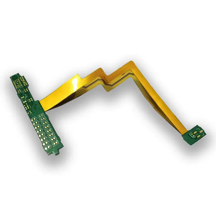
Medical Devices
The components for rigid-flex PCBs are placed in the supported areas of their structures, while flexible conductors follow narrow or curved paths inside hearing aids, implantable electronics, diagnostic assemblies, endoscopes, surgical instruments, and other types of medical devices. Flexible circuit boards connect sensors and displays to the compact control sections of these devices with significantly less space than wire harnesses. A major consideration for these devices is the repeated sterilization process; autoclave heat, steam, or chemical exposure can degrade the adhesive used to bond the coverlay material to the circuitry and cause it to lose adhesion or integrity after several cycles, even while the printed circuit board still passes a final quality control check. To support this, the documentation associated with the file set must include the sterilization method, cycle count, and routing configuration; the circuit design must include the bend duty; and lot traceability records must be included. Fine-feature fabrication and BGA/QFN X-ray inspection support the reliability requirements.
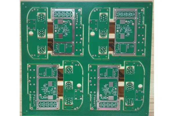
Aerospace and Defense
Aircraft avionics, satellite instrumentation, drone systems, and guidance electronics use rigid-flex PCB technology where multiple installation planes must be crossed with fewer discrete points of interconnection between circuits. Rigid-flex technology is often used for applications where controlled-impedance signals must be carried through a flexible transition while being exposed to vibration-driven flutter and thermal expansion; this combination causes mechanical stresses that would not be evident through a conventional signal-integrity check because impedance evaluation and mechanical qualification are typically carried out as separate tests. All drawings and qualification plans must identify whether impedance measurement and mechanical qualification will be evaluated as a combined method or as separate tests. Proper stackup control, tapered transitions, plated-interconnect verification, impedance evidence, inspection records, and AS9100D quality-system coverage support the application.
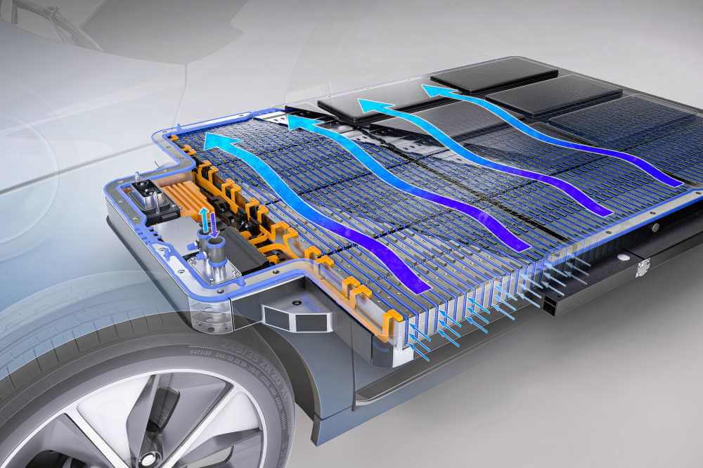
Automotive and EV Battery Systems
Rigid-flex PCB technology is used in ADAS cameras, radar, instrument clusters, and infotainment systems to maximize the available space within compact product housings and accommodate controlled moving features. Flexible circuitry in EV battery packs provides a means of connecting voltage and temperature sensors across a battery-cell array. In a long battery-sensing circuit, cumulative dimensional error can shift connector contacts away from the cell pitch, while conductor resistance and isolation performance affect measurement accuracy and safety margins. The quote package focuses on the dimensions that need to be defined for the cell pitch, connector datum reference system, and total conductor resistance. It also includes creepage and clearance requirements, temperature range, fold sequence, and end-to-end test points. IATF 16949 traceability is used as a manufacturing control.

Industrial Automation and Robotics
FPCs are used in robot joints, scanner mechanisms, inspection cameras, conveyor systems, long-reach sensors, and lighting systems. FPC designs for moving joints are based on determining the copper, radius, and transition designs using the bend axis and cycle target. The main risk is that a single-axis radius specification does not account for torsional loading combined with bending or reverse bending. This risk is increased if the bend axis moves during operation because the specified bend path may no longer represent the actual motion. The motion definition needs to be clear regarding the full travel path, twist angle, speed, dwell positions, temperature, and target cycles. Extra-long FPC can reduce harness breakage across an extended machine.
Consumer and Wearable Electronics
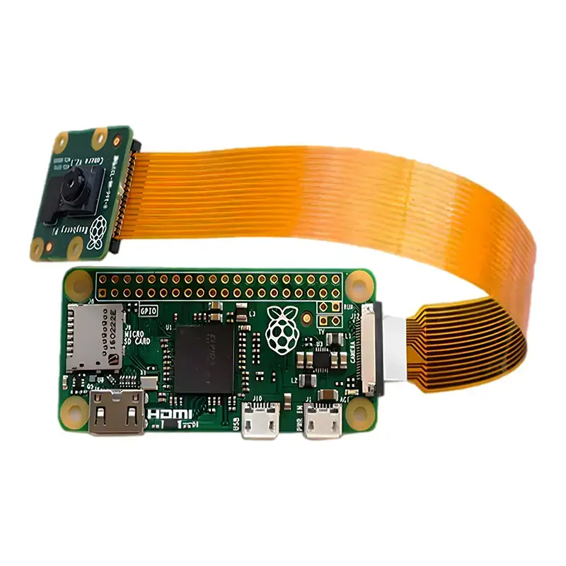
Foldable phones, laptops, compact digital cameras, fitness products, and wearable devices use FPCs in hinges, display edges, camera stacks, and body-conforming surfaces between multiple components within the same device. These devices use rigid-flex construction to connect multiple component zones within the smallest possible package. When a hinge bends, it often causes a shift in the bend axis of an FPC, and as the FPC is stressed, some areas may compress or twist out of position. A free coupon placed on a fixed mandrel does not reproduce the changing bending strains of the FPC; therefore, although it may pass a free-state test, the final assembly could fail after installation. The verification process must therefore test the entire enclosure or use an enclosure fixture that reproduces the actual installed motion. The stackup thickness, copper density, stiffener placement, and bend requirements determine whether the integrated structure is preferable to a replaceable cable.
Imaging and Communications Equipment
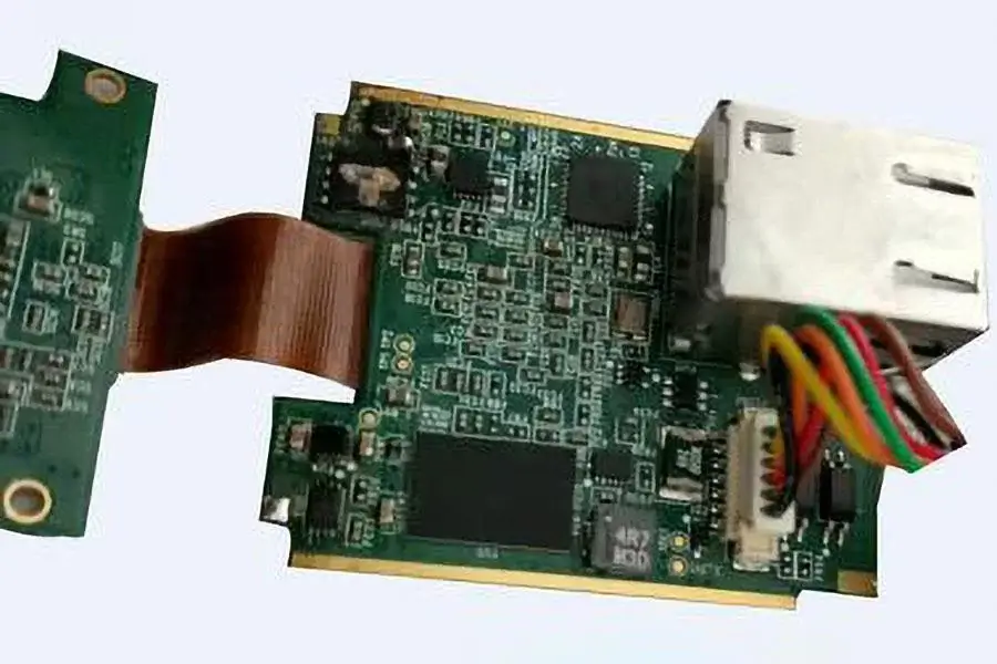
Medical imaging equipment, ultrasound probes, security scanners, baggage scanners, large displays, and communications equipment require conductors routed along long or three-dimensional paths to connect to power or signal sources. Extra-long FPCs may reduce the number of intermediate connectors that can fail, while rigid-flex circuit technology can route controlled signals between rigid RF or processing zones. The primary risk is the entire transmission structure; this includes rigid-to-flex transition geometry, reference-plane continuity, coverlay thickness, shielding termination, connector launch, insertion loss, skew, and the return-current path. The test process should specify whether impedance coupons, TDR, insertion-loss evidence, or only continuity and isolation data are required. Long-format registration and end-to-end electrical verification should also be included in the test plan.
Our PCBA Production Lines
















Rigid-Flex and Flexible Circuit FAQ
Yes. Mounting static components requires a stiffener, defined land geometry, strain relief, carrier support, and controlled placement and reflow. An important detail to include in the drawing is not just the general description of the “stiffened area,” but also the actual keepout boundary around it. A component pad placed slightly within the transition zone because of unclear keepout boundaries is a common reason for a design being returned during DFM review rather than assembled as drawn.
A stiffener is needed where a connector, component, or mechanical attachment point would otherwise load an unsupported flex section. Another consideration when including stiffeners in the drawings is the location of the transition edge between the stiffener and the flex area. This edge is a common location for concentrated bend strain, so its position relative to the active bend zone is as important as the material used.
Yes. The practical question for a quote is not whether controlled impedance is achievable, but whether the rigid and flex sections need separate impedance models. If the dielectric or reference-plane structures in the rigid and flex sections differ, a single impedance target across both sections is commonly inaccurate.
Both can be used on the same circuit; flexible solder mask is usually specified around fine-pitch pads, while coverlay can be specified for the bend area. The choice that most significantly affects cost and lead time is the location of the transition between the flexible solder mask and the coverlay relative to the required bend zone. Specifying this point in the drawing can prevent DFM questions before fabrication begins.
One key issue that is often overlooked during pricing is that the thermal assumptions used for continuous loads differ from those used for intermittent loads. A circuit designed to handle a brief peak current can become undersized if it must carry the same current continuously. The actual duty cycle must be provided so that current capacity can be calculated correctly.