Upload BOM & Gerber
-
Mobile: +86 13312967631
-
Email: sales@sugaintl.com

High Speed PCB Design
From High-Speed Requirements To Manufacturable PCB Decisions
High-speed PCB performance depends on stackup, impedance, materials and manufacturing working as one system.
50–100 MHz / <1 ns
1–56 Gbps Materials
USB4 / USB 80Gbps / TB5 80–120Gbps
100G / 400G / 800G Ethernet · 112G / 224G SerDes
What Is High Speed PCB Design?
High-speed PCBs have design and fabrication requirements that are different from ordinary interconnect boards. A PCB becomes high-speed when signal behavior, signal-edge rate, interface frequency, or data speed changes the design parameters from layout completion into manufacturing-sensitive signal-quality control.
The four categories of early screening signals are listed in the table for high-speed considerations. The same four conditions return as fabrication-verification triggers.
| Trigger condition | Example signals | Main risk | Next decision |
|---|---|---|---|
| Digital frequency above 50–100 MHz | USB3.2, HDMI 2.1, PCIe 4.0, DDR5 | Edge behavior can make trace geometry, impedance, and return path visible to the signal. | Controlled impedance and layout rules. |
| Rise/fall time shorter than 1 ns | Fast digital interfaces and clock/strobe groups | Timing, reflection, and skew may matter even when clock frequency looks moderate. | SI risks and delay/skew constraints. |
| Multi-gigabit serial links | PCIe 6.0 and 112G SerDes examples | Insertion loss, impedance mismatch, and eye diagram degradation can drive failures. | Review stackup, materials, and fabrication testing. |
| RF or analog frequency above 300–500 MHz | Wi-Fi 6, 5G, radar, satellite communications | RF/high-frequency concerns overlap with high-speed digital but follow different layout and material priorities. | Decide whether high-frequency PCB guidance is also needed. |
When A PCB Becomes High Speed
When the trace on a PCB becomes high speed, that trace begins to act as part of the circuit. The clock on the block diagram may look normal relative to the rest of the connections on that board, but fast rising edges may show the effects of impedance mismatch, broken return paths, timing skew, and radiated noise. That is why rise/fall times on a PCB become as important as the nominal frequency.
Digital And RF
High-speed digital PCB design does not equal high-frequency PCB design. They may begin from similar design concerns, but the focus is different. Digital work usually focuses on fast edges, serial links, memory timing, timing skew, crosstalk, and return path continuity. RF and high-frequency work focuses more on wavelength, radiation, controlled electromagnetic behavior, dielectric loss, and field containment.
The RF or analog frequency boundary is 300–500 MHz for designs such as Wi-Fi 6, 5G, radar, and satellite communications. Most of these products need digital-interface considerations on the same board that may also carry RF signals. In other words, these products are better treated as mixed-domain boards. DDR, PCIe, and USB belong under high-speed digital planning, while RF-dominant behavior belongs in high-frequency PCB guidance.
Signal Integrity Risks In High Speed Boards
| Risk | Typical trigger | Design lever | Production review |
|---|---|---|---|
| Reflection and impedance discontinuity | PCIe 6.0, PCIe 7.0 128 GT/s, 112G/224G-class SerDes examples; eye diagram degradation and bit errors | Controlled impedance, stackup continuity, transition design. | Impedance targets and layer transitions checked before production. |
| Crosstalk and skew | Length, delay, relative delay, skew, DDR timing violations | Spacing, topology constraints, matched timing groups. | High-speed signal groups constrained and checked by timing relationship. |
| PDN droop and ground bounce | High PDN impedance, insufficient decoupling, ESR/ESL at high frequency | PDN planning, return path continuity, capacitor selection. | PI risks reviewed in layout and manufacturing reviews. |
| EMI and compliance risk | Poor routing, improper shielding, insufficient grounding, common-mode radiation | Grounding, shielding, edge-field handling, routing discipline. | EMI-sensitive structures reviewed through fabrication or test attention. |
For example, a trace pair that appears perfectly matched in length can still fail timing because physical trace length does not equal propagation delay, so timing groups must be constrained by propagation delay, not only by visual match in layout. Also, PI failures, such as droop and ground bounce, may be confused with SI failures, because at higher frequencies a capacitor's real-world impedance (ZC < ZS // ZL) is dominated by ESR and ESL, rather than by its rated capacitance. Even well-balanced differential pairs may generate EMI due to the conversion of part of the differential signal into common-mode radiation through small layout asymmetry.

Controlled Impedance And Stackup Planning
Controlled impedance is more than a simple trace-width number. Controlled impedance is defined by stackup, dielectric data, return planes, return path continuity, manufacturing variation, and the ability of the manufacturer to adjust trace geometry or material thickness to meet the signal target.
| Signal class | Target example | Stackup input | Fabrication adjustment | Verification result |
|---|---|---|---|---|
| PCIe differential pair | 100 ohm differential impedance | Signal layer, return plane, dielectric thickness, copper weight. | Trace width / spacing may be adjusted under manufacturing tolerances. | Confirm impedance coupon or equivalent impedance record. |
| DDR3 / DDR4 single-ended memory signals | 45-55 ohm single-ended impedance | Layer assignment, return plane, length/skew group planning. | Stackup and material thickness changes may affect routing targets. | Confirm impedance target and timing group constraints before production. |
| Low-layer high-speed digital board | 4-8 layers as a low-layer example | Layer count rationale, power/ground plane pairing, routing channel density. | Standard or custom stackup selection affects cost and repeatability. | Confirm that layer count supports return path and routing density. |
| High-layer-count backplane / data-center-switch board | 32-42+ layer custom stackup as a high-layer-count example | Dense routing channel allocation, multiple isolated return/ground planes, controlled-impedance zoning across mixed signal groups. | Custom stackup and lamination sequencing usually require fabricator co-design before layer count is locked. | Confirm return-path isolation and impedance consistency across every signal layer, not only the outer layers. |
| Package-sensitive high-speed signal | over 500 MHz pin-package delay example | Package delay, BGA/LGA escape, board-level timing boundary. | Fabrication cannot fix package-board timing assumptions after layout. | Confirm timing assumptions before routing sign-off. |
Impedance Targets
The impedance target is derived from the requirement of the interface. The engineer translates the impedance requirement into the copper geometry that represents the board stackup.
Return Path And Plane Spacing Rules
The simple multiple-spacing rule shows that, at high speed, current returns via the nearest available reference structure, and that when a discontinuity occurs, that current must make a much larger loop.
Early screening can be beneficial. The current routing condition must be related to the high-frequency content of the high-speed signal, the signal edge rate, the routing density of the high-speed signals, and other layout conditions.
Standard Or Custom Stackup?
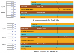
A standard stackup can be applied if the routing density, the impedance target, and the location of the return plane follow a repeatable pattern. This is true for most low-layer boards (4-8 layers) as long as the pairing of the layers stays consistent.
If a standard stackup cannot be applied, the only other option is a custom stackup. Custom stackups are used in applications with unusual dielectric thickness, tight impedance zoning, or very dense escape routing. Custom stackups also apply to backplane/switch boards at 32-42+ layers, where multiple isolated return planes compete for space with controlled-impedance zones. The routing decision must occur before routing resources are locked, which means that custom stackups can fix one signal group but still destabilize material sourcing. The lowest cost for negotiating with a fabricator regarding material, thickness, and tolerance is before routing is completed. After routing is completed, even a slight change in dielectric will introduce variations to the impedance, skew, and clearance of the signal being routed.
Package And Board-Level Timing Boundary
High-speed signals do not rely only on visible traces of the circuit board. The actual timing budget is shared by all elements of the silicon, package, BGA/LGA escape, and routing of the circuit board. As frequencies exceed 500 MHz, the delay between the pins and the package becomes large enough to matter. The PCB controls the geometry of the traces and the layer transitions of the circuit board. The timing assumptions made before use of the PCB cannot be corrected by fabrication of the PCB.
High Speed PCB Materials
The selection of materials for a high-speed PCB is based on many factors, including loss, dielectric stability, route length, frequency of the signal, link budget, and availability. It is still common to use FR4 materials for less demanding routes. However, if the route length is long, and if the requirement for low insertion loss for a high-speed link exists, then it may require low-loss laminate material or hybrid laminate stackups for manufacturing.
Dk And Df Loss Factors
Dk determines the impedance and propagation characteristics of a circuit because a signal does not just travel through copper, but also through the electromagnetic fields surrounding the traces. Df describes how much energy a dielectric material absorbs when the frequency of the signal rises.
The Dk and Df values are relevant only with complete usage context. Traditional FR4 is typically measured at 1 MHz, while high-speed links see a completely different frequency range of use. A manufacturer's datasheet can provide comparable information for high-speed links or mixed-material stackups, but a generic value may not describe the actual loss of the routed channel.

FR4 Limits At High Data Rates
FR4 is still acceptable for short routing lengths or less demanding interfaces with a forgiving loss budget; however, once the route length, frequency content, or the allowed insertion loss of the circuit board exceeds the capability of a typical FR4 material, specialized low-loss laminate materials or PTFE laminate compounds may be necessary for long serial routes and tight eye-margin targets.
Low-Loss Laminate Choices
Engineers can compare low-loss laminate material options by Dk, Df, Tg, availability, halogen-free status, and speed range; the following table provides material selections for stackup consideration; however, the data contained in this table must be regularly checked against current material supplier datasheets before being used for item quotes or stackup locks.
| Material code | Brand | Type / speed range | Dk | Df | Tg | Halogen-free | Datasheet | Use boundary / procurement note |
|---|---|---|---|---|---|---|---|---|
| IT-988G SE | ITEQ | 40-56 Gbps | 3.2 | 0.0025 | 190 (DSC) | Yes | IT988GSE.pdf | Low-Dk / low-Df material option; confirm project availability before committing stackup. |
| R-5785N/M7N | Panasonic | 40-56 Gbps | 3.3 | 0.002 | 200 (DSC) | No | R5785N(M7N).pdf | 40-56 Gbps material option; verify lead time, laminate availability, and stackup compatibility. |
| TU-933 | TUC | 25-40 Gbps | 3.4 | 0.0025 | 170 (TMA) | No | TU933.pdf | 25-40 Gbps material option; confirm whether loss budget and thermal needs match. |
| Tachyon 100G | Isola | 25-40 Gbps | 3.02 | 0.0021 | 215 (DSC) | No | Tachyon100G.pdf | Low-loss material option; pair selection with route length and insertion-loss margin. |
| IT-968 SE | ITEQ | 25-40 Gbps | 3.3 | 0.0038 | 185 (DSC) | No | IT968SE.pdf | 25-40 Gbps material option; compare Df against link budget before selection. |
| R-5785/M7 | Panasonic | 25-40 Gbps | 3.6 | 0.003 | 200 (DSC) | No | R5785(M7).pdf | 25-40 Gbps material option; confirm fabrication data and availability. |
The table above keeps each material row separate because one label, "lowest loss," obscures significant distinctions. Not all 40-56 Gbps materials with a very low Df will address all boards if that material is not available, is difficult to place in the selected laminate stackup, or is unnecessary for the routing length. The 25-40 Gbps material is frequently the best design choice when the loss budget permits.
Material Trade-Offs And Hybrid Stackups
The lowest-loss laminate with an acceptable level of performance will protect the target margin while providing adequate performance given its characteristics, such as the laminate's ability to be fabricated, availability for purchase, thermal behavior, repeatability in the same laminate stackup, and matching properties with the other materials in the laminate stackup. Examples of mid-loss materials with acceptable performance are Isola FR408HR and Panasonic Megtron 4 for links up to approximately 10-16 Gbps; there is a more expensive material class for high-speed links, but if the channel does not require such a high-performance material, then that material may unnecessarily increase costs or create sourcing or laminating challenges that the project did not account for.
Hybrid stackups allow low-loss materials where they are critical and use other, more common materials where the signal requirements are reduced.
Design consideration for hybrid stackups only works when impedance, laminate performance, and compatibility of materials have been verified as a complete system rather than on an individual laminate basis.
High Speed PCB Layout Rules
Rules for high-speed PCB layout cannot be effectively developed without considering how the rule relates to the signal type or class, target impedance, timing group, and laminate stackup. Mnemonics, such as the example of 3W, can be useful tools for assessing the high-speed PCB layout; however, they do not replace the specific constraints associated with each signal type or class.
| Review item | What it protects | Design basis | Practical use |
|---|---|---|---|
| Route differential pairs as a controlled signal group | Reflection, crosstalk, pair imbalance | USB, HDMI I/O, PCI Express buses, DDR clocks/strobes examples | Apply the confirmed impedance and topology targets during routing. |
| Set spacing by signal class and stackup | Crosstalk and unwanted coupling | 3W rule / trace spacing review | Use 3W as a screening rule, then confirm spacing against signal class and stackup. |
| Lock trace geometry after stackup is known | Impedance drift and manufacturing tolerance mismatch | Trace width / spacing adjustment under manufacturing tolerances | Recalculate width and spacing if stackup or material changes. |
| Match delay and skew groups | Timing violation in DDR and source-synchronous interfaces | Length, delay, skew terms | Constrain clocks, strobes, and data groups by delay and skew relationship. |
| Use topology constraints from the interface | Bad routing order, stubs, and constraint conflicts | SDRAM, PCI Express, USB application notes; JEDEC | Use interface notes to set routing order, branch structure, termination, and stub limits. |
| Treat corners and vias as conditional risks | Impedance discontinuity and via-stub loss | 90-degree corner and via-stub guidance | Confirm whether geometry and via stubs create meaningful discontinuity for that signal class. |
Differential Pairs And Timing Groups
Controlled group routing of high-speed signals is preferred over individual-signal routing. Signals, such as differential pairs, DDR clocks, and timing-critical nets, demand impedance, pair spacing, skew, and return current that need to be treated together. The appearance of a clean route does not mean that a failure will not occur if two conductors see variations in the reference conditions, or if the delay model is not properly aligned with the stackup.
Spacing, Geometry And Stackup
Spacing rules, for example, 3W, are screening criteria; the actual spacing requirements for a signal class are determined by stackup height, signal class, routing layer, trace length, edge rate, and physical proximity to aggressors. The question is not, "Is there 3W spacing?" but instead, "What spacing does the signal class require with the particular stackup?" Trace width and spacing can only be definitively established after locking down the stackup, dielectric thickness, copper weight, and impedance target; if material or layer thicknesses change after establishing width and spacing, the geometry will need to be recalculated.
Topology Constraints
Topology rules are specific to each interface and define routing order, the configuration of branches, placement of terminations, and stipulations on stubs before routing. For example, the order of connections, or too large a stub, could result in SI loss for interfaces like SDRAM, PCI Express, USB, etc., where the receiver may reject invalid connection orders. For a 90-degree corner or via stub, the latter can be very risky under certain conditions; however, a 90-degree corner will not necessarily destroy the signal, as the way in which it is routed and the frequency of the signal determine the impact of the corner. Similarly, via stubs introduce additional risk to the channel when its margin is tight enough to make the extra discontinuity a concern.
Corner And Via Myths
Corner and via recommendations depend on signal class, channel margin, geometry, and frequency content, as descriptions of any corner, specifically 90-degree corners, require caveats to cover certain conditions, such as trace width, or limit the effect to factors such as 10% for varying frequencies. The language or requirements surrounding a corner represent extreme conditions, and they only become relevant for very high-speed signals with high-frequency content; otherwise, most digital clock rates fall below this criterion.
Via recommendations require the same level of discipline. A via can be acceptable by providing a return current path, even for a signal operating at moderate speeds. However, if a via is unused, there is a risk of introducing an unwanted stub discontinuity. If there are very tight channel margins and a demanding signal class, eliminating vias and minimizing stubs may be more critical.
Fabrication Reviews That Protect Signal Quality
| Review item | Protects against | Design input needed | When to verify | Verification basis |
|---|---|---|---|---|
| Pre-layout, DFM and post-layout verification | Late stackup changes, routing density issues, unchecked constraints | Functional requirements, schematic capture, PCB layer stack | Before routing and again before production | Stackup, constraint, and manufacturability review |
| Back-drilling and via-stub review | Stub resonance, discontinuity on ultra-high-speed paths | Via structure, layer transitions, high-speed net list | During fabrication planning and drill data review | Drill data, layer transitions, and high-speed net class |
| EMI and edge-field review | Edge radiation and overconfident rule use | Plane geometry, return path, board-edge structures | During layout review and fabrication data review | Board-edge geometry and return-path review |
| TDR and eye diagram testing | Impedance and link-margin uncertainty | Test channel, PRBS pattern, impedance target, coupon or structure | Prototype or selected high-speed validation stage | Impedance and link-margin validation |
| Surface finish, lamination and registration review | Loss, misregistration, drilling/etching tolerance impact | Material stackup, copper features, via plan, surface finish choice | Before production data is finalized | Process-control review before release |
The same four screening conditions carry different verification weight once the design moves toward fabrication:
| Signal class / trigger condition | Design signal | Verification priority | Note |
|---|---|---|---|
| Digital frequency above 50-100 MHz or rise/fall time shorter than 1 ns | Fast-edge screening condition | Recommended: pre-layout/post-layout DFM verification | This is a screening trigger. Start with design verification instead of forcing advanced tests on every net. |
| Multi-gigabit serial links such as PCIe 6.0/7.0 and 112G/224G-class SerDes | Reflection and eye-diagram risk | High priority: TDR, eye diagram, back-drilling / via-stub review | Reflection and eye closure risk justify impedance and link-margin result. |
| RF or analog frequency above 300-500 MHz | EMI and RF-adjacent risk | Recommended: EMI/edge-field review, including 20-H boundary review | The review depends on board edge, return path, and field behavior. |
| High-layer-count custom stackup, such as 32-42+ layer backplane or switch-board class work | Stackup and registration risk | High priority: surface finish, lamination, and registration precision review | More layers increase the effect of lamination and alignment tolerance on impedance consistency. |
Pre-Layout, DFM And Post-Layout Verification
Fabrication planning begins before routing, including stackup, material selections, routing density, and connecting those to signal quality. Before any routing is committed, the functional requirements, schematic capture, and PCB stack need review.
Pre-layout verification will help identify any mismatches between the interface, number of layers, types of materials, and density of routing. DFM review verifies that this design can be manufactured within its intended process window. Post-layout verification is a second opportunity to validate traces, via structures, clearance distances, and constraints as they have become physically realized within the designed PCB.
Back-Drilling And Via Review
The importance of back-drilling and via-stub review is greater for high-speed signals than for non-high-speed signals because a change of layer for a high-speed signal may leave behind an unused via barrel that may act as a resonant stub. Ultra-high-speed signals may also suffer more as a result of this discontinuity because they will experience greater degradation of insertion loss, reflection, and eye margins.
The decision for a routing solution involves consideration of the class of signal, the type of layer transition, the remaining stub length, the stackup configuration, and the margin of the channel.
EMI And Edge-Field Review
The 20-H rule is used as a concept to minimize edge-field emissions, or radiation from a PCB, by placing the power plane some distance from the edge of the PCB and ground plane. Experimental test data has shown a reduction of emissions, although this has been shown to be very sensitive to the specifics of the board geometry and the method of measurement.
The board characteristics, the return current path, and the board structure will ultimately determine if there is a field-coupling problem. An RF/mixed-signal PCB, which typically has a considerably higher emissions risk than low-speed digital technology, receives greater attention than a low-speed hybrid low-radiation-risk PCB.
TDR And Eye Diagram Testing
TDR and eye diagrams will give different responses to different questions; TDR provides a way to identify and locate impedance discontinuities along a trace or coupon structure. Eye diagram results indicate if there is still enough timing and voltage opening under the selected test condition, pattern, and channel at the receiving end of the link.
Project deliverables, in addition to the use of standard PRBS patterns, also include the construction of test structures, links to their use in test channels, and the resultant eye diagrams from received signals to show link margin on a project under development. For example, for the advanced planning of a high-speed data center, it may be necessary to devote greater thought to the test channel design for the validation of a 224G-class channel than with ordinary controlled-impedance designs.
Surface Finish, Lamination And Registration Review
The manufacturing quality can preserve the high-speed assumptions that remain after the design has been created; the etching tolerances can determine the width of the PCB traces, while drilling will affect the geometry of vias, and registration will affect the alignment of layers and the consistency of the return path. Finally, lamination will affect the thickness of dielectrics and the repeatability of their impedances.
The selection of the surface finish must also be considered since it affects signal integrity and reliability of the production assembly, particularly when the designs include small geometries or densely populated features; the choice of finish must match the signal and assembly requirements of the board and not made only from historical reference.
High Speed Interfaces And Applications
High-speed PCB design will be determined by the behaviour of the interconnections; each of the following interfaces supports high-speed design, however, each requires specific combinations of impedance, loss, skew, materials, and fabrication evaluations and will also present unique failure characteristics that will differ from one another: DDR, PCIe, SerDes, USB, HDMI, 5G adjacent electronics, edge AI, sensor fusion, IIoT, and rugged electronics.
DDR And Memory Interfaces
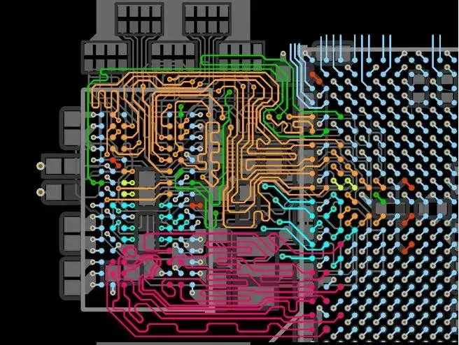
DDR3/4/5 memory interfaces can push high-speed PCB layout decisions based on clocking, strobes, source synchronous timing, skew control, and return path discipline. DDR5's on-die termination results in a different effective impedance at the connector than DDR4. While a copy of DDR4's layout rule set may pass design rule checking for DDR5, it does not guarantee passing for DDR5. The single-ended 45-55Ohm impedance ranges are planning references, not universal memory values.
PCIe And SerDes Boards
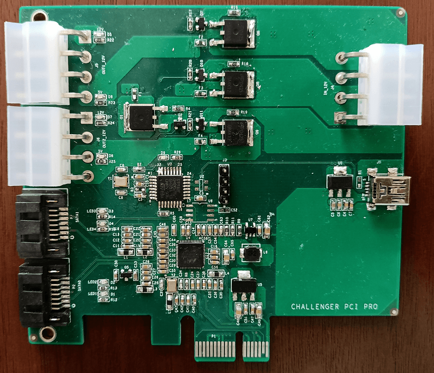
Channel loss, controlled impedance, routing lengths, connector transitions, and test confidence drive the design of PCIe and SerDes boards. The same connector transition or via stub that was ok when operating at a lower data rate will create a reflection point at the next serial-class data rate due to the new channel conditions. planning the channel before layout lock is critical; any needed changes must occur before then.
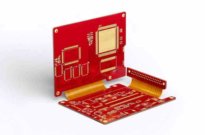
Display And Peripheral Links
USB3.2 at 5Gbps (USB3.2 Gen1/USB 3.0), USB3.2 Gen2 at 10Gbps, USB4 at 40Gbps, USB4 v2.0 / USB 80Gbps, Thunderbolt 5 at 80Gbps of bidirectional bandwidth/boosts up to 120Gbps, HDMI 2.1 at 48Gbps, HDMI 2.2 (Ultra96) up to 96Gbps, MIPI, USB-C, etc., have drastically different connector geometries, controlled impedance, skew, and routing density considerations. The elements linking the connector and trace are where most link failures occur; that is, if there is a failure in link connectivity, it will typically occur at the USB-C receptacle connectors in the form of lane remapping resulting from cable orientation flip. Lane remapping works by having the routing structure that supports lane routing located within two separate physical locations, requiring multiple routing paths from the connector instead of just one. It is also possible for the lane remapping to simulate and pass successfully, based upon a skew budget, yet fail once in the field environment.
5G And RF-Adjacent Systems
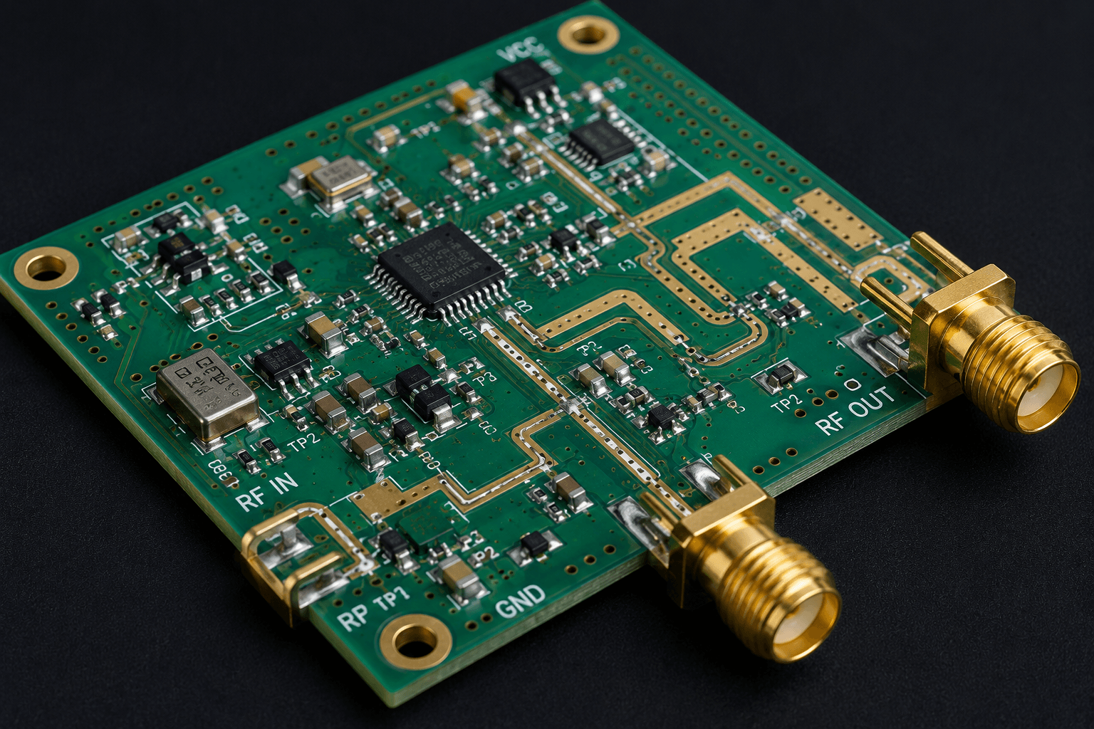
5G mmWave, Wi-Fi 6/Wi-Fi 7, radar, and satellite electronics can share a board stackup with high-speed digital interfaces. High-speed digital interfaces and other RF-adjacent technologies may have different stackup and material requirements.
Edge Computing And Embedded AI Boards
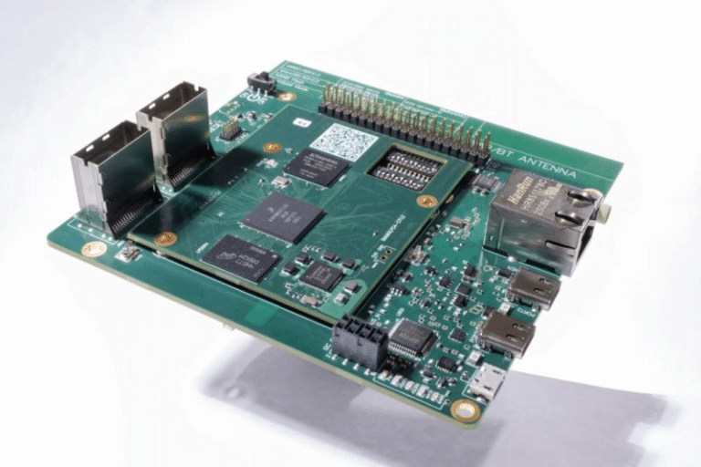
Embedded AI boards and edge computing systems can include MPU or custom application processors, FPGAs, memory interfaces, storage, and high-density power delivery. System density will put maximum stress on those boards. An example of maximum stress can be found on boards that have many connection pins for the AI accelerator — a high fan-out BGA — and the memory interface. Often, both connection types occupy the same layer pair of the same board, resulting in escape-routing conflicts.

Mil-Aero, Space 2.0 And Robotics Electronics
Mil-aero, Space 2.0, industrial, and robotics electronics are systems that can raise the cost of a failure caused by poor signal quality due to the combination of vibration, ESD, ruggedized assembly, and different qualification requirements along with high-speed routing. Standards such as MIL-STD-461, DO-160, and IPC Class 3/3A apply as project requirements when the documentation confirms them. Vibration and thermal cycling over time can affect via barrel plating and result in intermittent failures that were not evident during qualification testing and were not caught by the one-time electrical test performed at qualification.

Sensor Fusion And Multi-Board Systems
Multi-board systems and sensor fusion are unique to each system and sensor combination, and the design of multi-board systems and their sensors changes the material, connector, and routing selections for the system, as the requirements for interfacing with each sensor are not the same for all sensors. In a multi-board system, the board-to-board connector is usually the weakest link in the chain; although the board's internal routing may support high performance, it can still fail in the field due to the connector footprint introducing an impedance mismatch and causing signal loss that the simulation did not model.
IIoT And Networking Boards
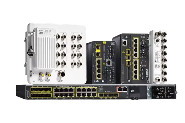
IIoT, 100GbE / 400GbE / 800GbE interfaces, the 800G / 1.6T Ethernet roadmap, optical transceivers, NVMe SSDs, and 112G / 224G-class SerDes combine long service lives with high-speed interfaces. A board that is qualified for 224G-class SerDes at the time of delivery can experience performance degradation toward the end of its expected life if the laminate's Df changes over time due to humidity absorption or thermal aging. Thus, the loss budget calculated during qualification will not be automatically fulfilled five years later.
How To Choose A High Speed PCB Design Partner
Choose a high-speed PCB partner who can bring together impedance, stackup and material information, routing constraints, fabrication verification, test results, qualification requirements, and production schedule before locking any risk into the PCB.
| Buyer question | Records | Risk covered | Where it reduces risk |
|---|---|---|---|
| Can the partner support controlled impedance beyond a nominal target? | Impedance adjustment and verification, single-ended/differential pair review, tolerance-aware trace geometry. | Reflection, pair imbalance, manufacturing variation. | Impedance planning and layout execution |
| Can the partner connect material data to stackup production? | Material datasheets, Dk/Df/Tg, core/prepreg thickness, procurement availability, standard/custom stackup rationale. | Insertion loss, unstable impedance, unavailable laminate. | Material and stackup selection |
| Can the partner show fabrication and test records for high-speed features? | DFM report, TDR, eye diagram, back-drilling review, sample or test-channel records. | Via stubs, impedance uncertainty, test gap. | Fabrication and validation |
| When is partner involvement needed? | Functional requirements, schematic capture, PCB layer stack before routing, pre-layout/post-layout simulation timing. | Late stackup changes, missed constraints, production delay. | Stackup planning and production release |
| Which standards or qualifications apply to the project? | Applicable ISO, AS, IPC-A-610J, IPC-A-600M, IPC-6012F, NADCAP, ITAR/JCP, MIL-STD, DO-160, IPC Class 3/3A project requirements. | Qualification mismatch and project-fit risk. | Application and reliability requirements |
| Can schedule claims be tied to realistic NPI records? | Prototype, NPI, and production timing examples, including ranges such as 2 days to 2 weeks for some NPI-to-production cases. | Unrealistic lead time and transition risk. | Production planning |
| What red flags stop selection? | No impedance question, no stackup confirmation, no Dk/Df discussion, no test records, no return-path explanation. | Supplier mismatch for high-speed work. | Supplier selection |
Impedance Support Records
The objective of impedance support documentation is for the target to correlate impedance within the electrical stackup, copper geometry, and manufacturing tolerances. A single nominal impedance value doesn't address how that nominal value will fare when it has been affected by variations in materials or layers.
Support records for impedance may include: Impedance calculation results with supporting notes, coupons or other means to measure copper impedance, verification of paired differential pairs, and records of width/spacing adjustments. Electrical stackup and material review before producing any board.
Stackup And Material Review Before Production
The manufacturer of the selected materials can show that these materials have electrical characteristics that are consistent with the development of a board, which supports the impedance and loss budgets, when placed in a repeatable build process. The manufacturer provides the existing stackup, together with reasons why that manufacturer has developed that particular electrical stackup. There may also be other reasons why a different custom stackup will need to be created for an application. In addition, materials may become unavailable or at least not available in time for manufacturing, and the electrical stackup is not locked in. If multiple stackups will accept the same routing, it's important to ensure that the stackup is robust in the design and provides the manufacturer with the expected design conditions for all variations.
Test Records For High-Speed Features
Not every signal type has to carry the same level of validation record. For example, a TDR signature/trace will typically be sufficient to confirm controlled-impedance digital traces. However, multi-gigabit serial links, for example, need eye-diagram or PRBS signature/data confirmation of their signals, in addition to TDR confirmation. Although TDR may provide accurate measurement data, cumulative losses or jitter may cause eye diagrams to have poor quality for proper conclusions or decisions. Also, requesting the same process for every board produced will incur additional cost with no increase in confidence.
When To Involve The Supplier
Supplier involvement works best during fabrication review of functional requirements, schematic capture, and layer stack decisions so incorrect constraints, late resource additions, and delays can be prevented. The early review determines if the layer count, materials, impedance targets, and routing density for the proposed PCB can be manufactured in the production window of an actual fabrication process. The timing analysis at the completion of the PCB layout matches the layer count, materials, impedance targets, and routing density as determined in the early review and does not require changes to the layout related to each of these parameters.
Once all high-speed routing has been locked, if the supplier is requested to re-evaluate anything regarding the PCB layout, the cost associated with making such changes grows significantly. If all of the layers have not been defined with the supplier before layout completion, then the layout is already predetermined by assumptions.
Qualification Requirements
When referencing these qualification requirements, the PCB manufacturer should recognize that these references are not interchangeable. IPC-A-610J covers acceptance of assemblies after construction, and IPC-A-600M covers acceptance of bare PCBs. The PCB manufacturer quoting either standard does not guarantee compliance with both standards. While NADCAP supports the process involved in PCB production, it addresses the control of that process, rather than a design requirement associated with the PCB. While projects reference MIL-STD and DO-160, these references have value when directly linked to a test method that a project needs.
Depending on the application for the PCB being produced, there may be multiple qualification standards that apply. For instance, for an electronic assembly going into an aerospace application, the applicable qualification standards would differ from those for a medical application. Qualification documentation belongs to the specific application of the PCB, rather than used as a checklist of qualification requirements.
Lead-Time Records And NPI Conditions
Most PCB manufacturers provide a headline stating the fastest time-to-market with an NPI product. PCB manufacturers will typically describe this as standard material, standard stackup, and no test channels.
Red Flags In High-Speed PCB Suppliers
Some of the red flags of a PCB supplier include a lack of impedance discussions, no confirmation of stackup, no discussion of Dk/Df, poor explanation for return path, lack of DFM or test records, and treating FR4 and low-loss laminates as if they are interchangeable materials.
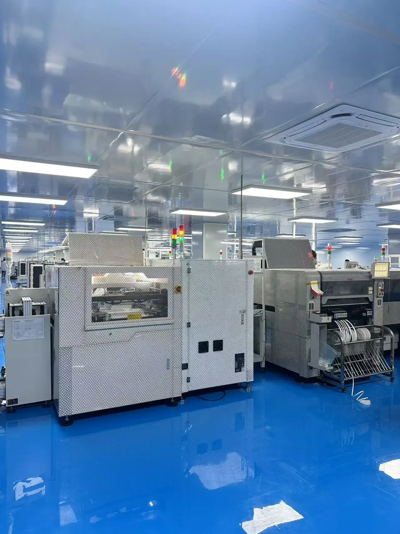
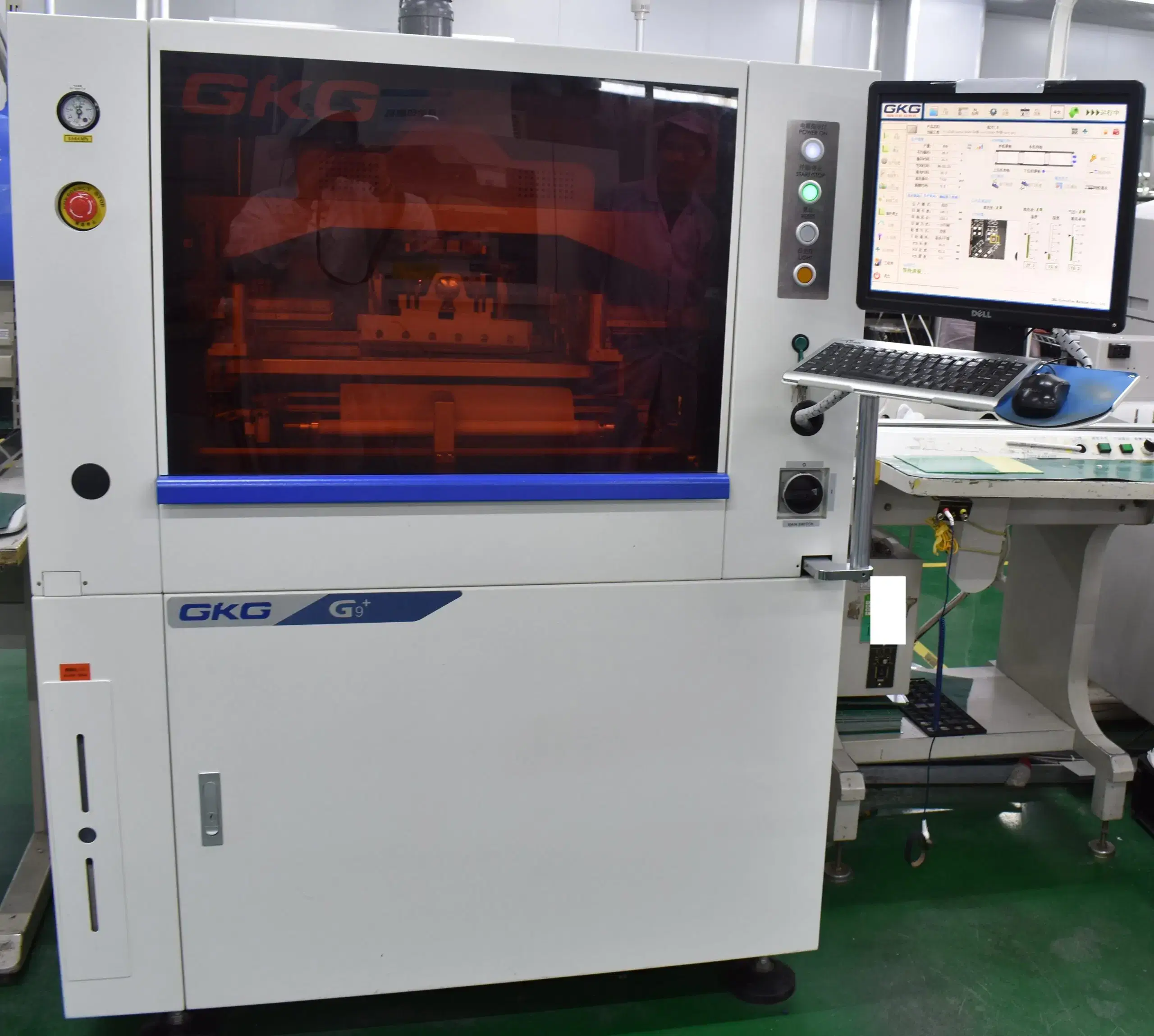
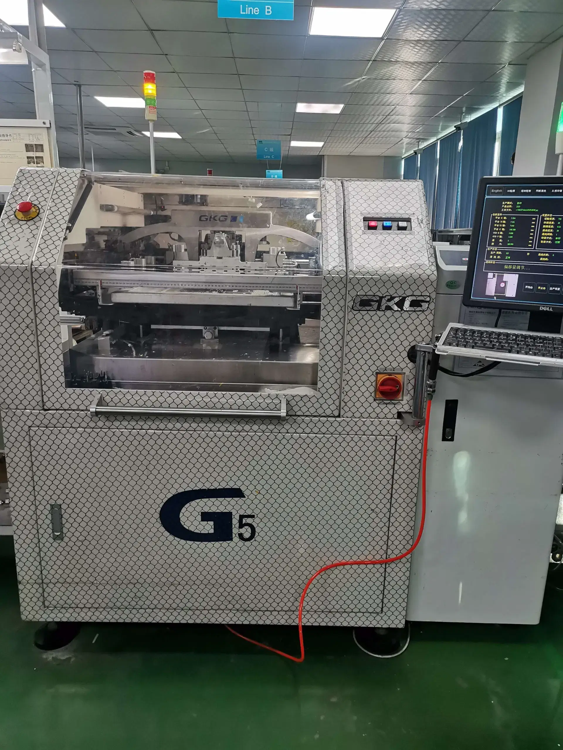
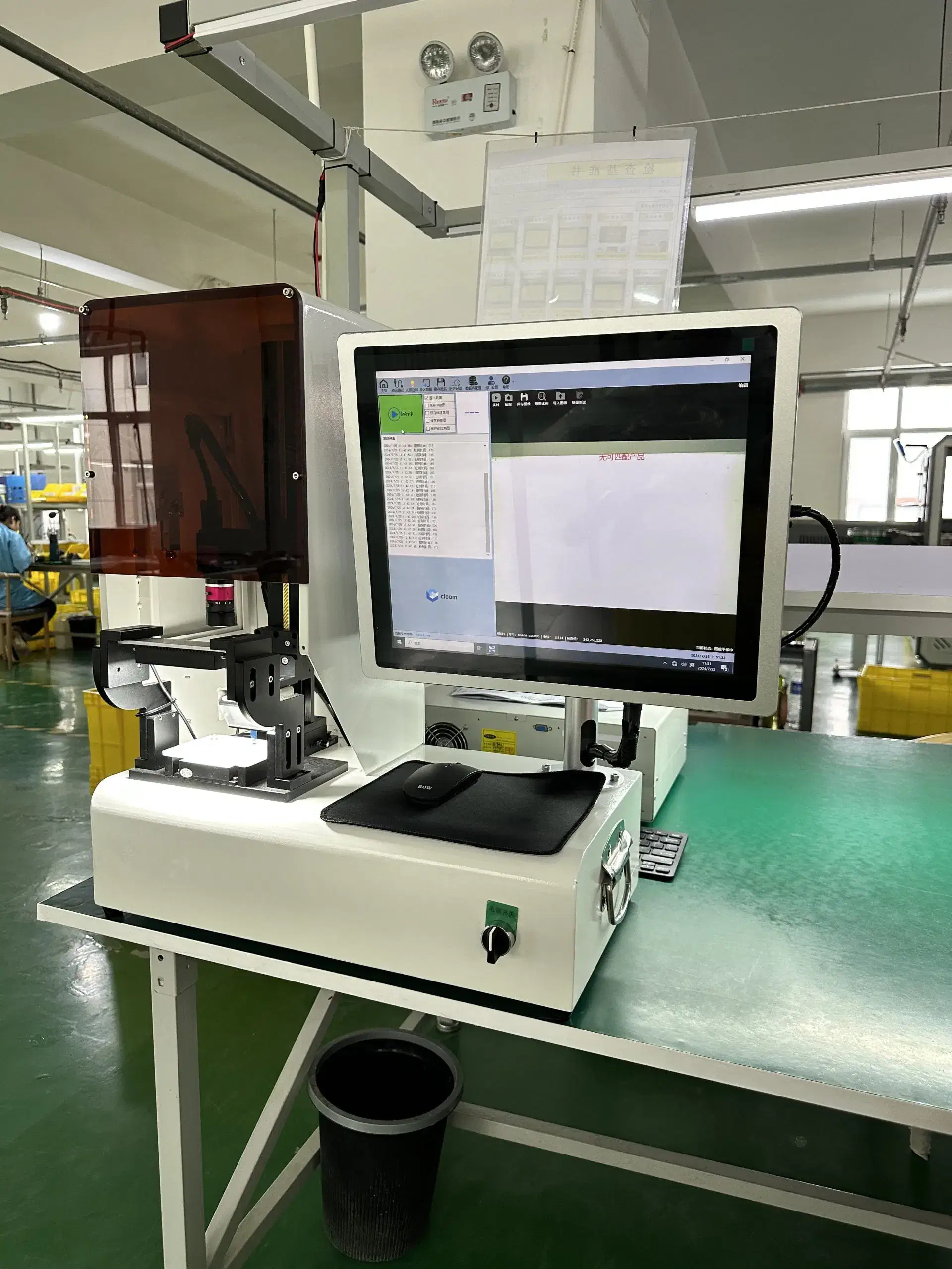
Our PCB Factory Gallery


Frequently Asked Questions
No. A 6-layer PCB can support high-speed designs when properly stacked up. The quality of the stackup, the types of return planes used, the density of the routing, target impedance, return path continuity, and interface speed represent the basis of what will affect the overall quality.
Yes, high-speed circuits can coexist on the same board as long as the high-speed nets have been appropriately designed for stackup, impedance, return path, spacing, and timing review when necessary. Do not apply high-speed guidelines to every trace; apply them based on how the signal is expected to perform.
Stitching vias may be necessary where there are layer transitions, return-plane changes, shielding, or return-path continuity issues. If there are no substrate issues, stitching vias may be decorative and do not add them to every layer; however, the stackup and return-current path will need to be analyzed to determine if placing stitching vias adds additional design complexity or reduces the overall risk of the substrate.
High-speed PCB design typically focuses on fast digital edges creating serial links; timing related to memory, differential signaling, signal integrity, etc.; and impedance-skew. High-frequency PCB design typically addresses RF characteristics and behaviors, radiation, dielectric losses, wavelengths, and controlled electromagnetic performance. Some boards may require both design types.
Most current high-speed designs still focus on PCIe 6.0 and 112G-class SerDes as a practical design baseline. PCIe 7.0 at 128 GT/s and 224G-class SerDes are risk anchors in the planning stages of future designs and are not yet targets for every current design. Consider these as future indicators for material and stackup risk.