Upload BOM & Gerber
-
Mobile: +86 13312967631
-
Email: sales@sugaintl.com

Conformal Coating & Potting PCB
Protect PCB Assemblies With Material Choice, Masking, Curing And Inspection
A conformal coating PCB decision starts with the operating environment, then moves through material choice, keep-out control, cure conditions, and inspection records. Get the environment-to-material match wrong, and no amount of careful masking or curing downstream will save the assembly.
25-250 μm Coating Thickness
0.1-0.3mm Bake-Cured Band
60°C Pre-Bake Step
80-110°C Heat Cure Range
7 Materials Covered
8 Standards Cited
12 Application Scenarios
9 Inspection Checks
What Is PCB Conformal Coating?
Conformal coatings are used to protect electronic components from environmental contaminants, moisture, and mechanical damage. They can help improve product reliability and performance and extend the life of electronic products.
| Concept | Definition | Exclusion | Decision |
|---|---|---|---|
| Conformal coating | Protective polymer coating that protects assembled PCB | It is not the same as surface finishing or complete encapsulation | Choose the material, process, and inspection plan for conformal coating |
| PCB surface finish | Metal finish used on PCB pads before assembly | It is not used as a coating over assembled components | Belongs to pad finish selection, not coating selection |
| Potting | Resin-based enclosure that provides superior protection | Makes inspection and rework difficult compared to conformal coating | Compare protection level, weight, and inspection access |
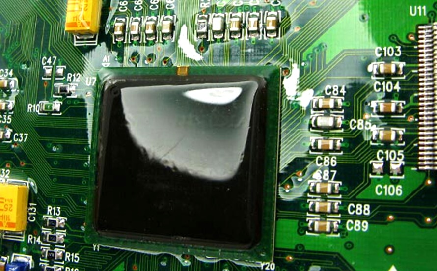
Protective Film, Not Surface Finish
The practical difference between conformal coating and surface finish is that the root cause of any assembly failing continuity or solderability tests is the surface finish, not the coating. Surface finishes are applied before the components are soldered; therefore, a solder joint failure cannot be attributed to conformal coating. Conformal coatings remain visible and inspectable after application, and they also take the shape of the board while allowing functional access areas to remain free from obstruction.
Moisture, Dust, Chemical And Thermal Risks
Conformal coating is often used whenever assemblies are exposed to humidity, dust, chemical vapor, fluctuating temperature, leakage risk, and mechanical contamination. Outdoor sensors, appliance controls, industrial electronics, vehicle modules, marine equipment, and miniaturized boards are examples of applications for conformal coating. There is nothing that can be done with a coating to fix upstream issues related to incorrect trace/pad spacing, contamination trapped under components before coating, enclosure leakage, or using materials with inappropriate exposure profiles. Coating is applied as a last layer of defense; it cannot substitute for properly designed boards or enclosures.
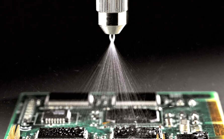
When Coating Is Not Enough
Coatings enable thin, inspectable, easily repaired protection. However, once exposure to sustained water pressure, extremely high shock loading, tamper resistance, or complete submersion occurs, an enclosure or a potting compound must perform functions that thin protective films 25-250 micrometer cannot. Coated PCBAs can easily be inspected and repaired, whereas potting material requires trade-offs for its higher and more uniform protective ceiling; they are two different protection choices, not competitors for the same purpose.
Conformal Coating Materials
Acrylic, silicone, polyurethane, epoxy, parylene, and fluoropolymer coatings offer solutions for many different types of exposure. The most common design selection mistake is choosing a coating without first verifying the exposure profile. Exposure characteristics necessary to make an informed selection include humidity, temperature, chemical exposure, abrasion, flexibility, repair access, coating thickness, and the inspection method required for the product.
| Material | Best Fit | Strengths | Watch-outs | Inspection |
|---|---|---|---|---|
| Acrylic | General protection, fast rework, fast drying | Easy rework; fast drying; good humidity resistance; high fluorescence | Viscosity drifts as solvent evaporates; flammable; can revert under heat + humidity | Visual / UV coverage; humidity exposure; rework access |
| Silicone | Thermal cycling, vibration, UV, flexible assemblies | High dielectric strength; fair moisture/abrasion resistance; stable across wide temperature range | Short pot life; limited solvent-vapor protection; humidity-dependent cure | Cure condition; edge coverage; UV/visual check; contamination control |
| Urethane | Chemical, moisture, abrasion, solvent resistance | Good dielectric properties; solvent-resistant; abrasion-resistant | Viscosity drifts in use; flammable; isocyanate exposure needs handling controls | Chemical exposure fit; removal plan; adhesion check |
| Epoxy | Higher protection where rigidity is acceptable | Useful to roughly 150°C / 302°F; high chemical and abrasion resistance; good dielectric properties | Chloride contamination risk; mix-ratio errors leave it under- or over-cured; rigid and hard to rework | Mix control; rework boundary; temperature cycling risk |
| Parylene | Ultra-thin, uniform coverage on complex geometry | Minimal added mass; low outgassing; no pinholes or bridging; biocompatible grades available | Batch vacuum process; needs a peelable mask before deposition; removal needs specific equipment | Process fit; masking plan; SIR / dielectric check |
| Amorphous fluoropolymer | Specialty low-dielectric or low water-sorption cases | Low dielectric constant; high glass transition temperature; low water sorption | Needs special solvents to remove; thin film limits; needs adhesion surface treatment | Material fit; adhesion check |
| Parylene HT | Specialty high-temperature, low-dielectric applications | Dielectric constant ~2.28; stable to roughly 450°C / 842°F; strong UV stability; excellent uniformity | Batch vacuum process; slower deposition; specialized equipment for removal | Process fit; deposition capability; rework boundary |
Acrylic For General PCB Protection
You should use acrylic if you need quick rework and visible inspection instead of extreme heat or chemical resistance. Reversion occurs when a cured film becomes tacky or soft again after being subject to combined heat and humidity conditions during storage or in the field. A PCB left in a warm and humid environment has a greater chance of reverting than boards in dry, temperature-stable locations. Since reversion is solvent-reactivatable, if reversion occurs on a PCB with an acrylic coating, a technician can typically strip the coating off the component and recoat it with the same thinner used to apply the coating, rather than having to mechanically or thermally remove epoxy as in other coatings.
Silicone For Temperature And Vibration
Silicone offers a flexible solution to the problem of component mismatch when PCB components, solder joints, and PCB materials expand differently under thermal cycling or vibration. Due to the short pot life of silicone, you usually require a two-component metering system rather than hand mixing to produce at volume. Cross-contamination is also the quieter issue: if silicone residue is transferred onto a PCB from gloves, tools, or a common spray booth and that PCB is coated with another type of coating, the second coating may not adhere properly. Because of the potential for cross-contamination, silicone lines are typically kept physically separate from other material production lines.
Urethane And Epoxy For Harsh Exposure
Both urethanes and epoxies trade rework ease for stronger protection. Urethanes based on isocyanate can require respiratory protection while being sprayed, and the viscosity must be periodically checked as solvent evaporation can cause viscosity shifts. Unlike other resins and adhesives, epoxies are less tolerant of mistakes within their mix ratios. Under-catalyzed epoxies may never reach a fully cured state due to remaining tackiness, while over-catalyzed epoxies are frequently too brittle to be utilized. Once epoxies have been properly cross-linked and cured, they cannot be dissolved by any type of solvent; therefore, mechanical means will have to be employed to rework an already cured epoxy, such as grinding, hot-air removal, or micro-blasting instead of wiping the epoxy with thinner.
Parylene For Thin-Film Coverage
Parylene provides thin coverage with consistency across complex board geometries, including medical electronics, sensors, MEMS, and lab-on-chip boards with tight spacing. Boards will typically be masked using a peelable dip-mask or tape before entering the vacuum chamber, and since deposition is a batch process, turnaround time is measured in hours for a complete chamber cycle versus minutes for a single spray pass. Parylene is most often applied to lower-volume, higher-value boards rather than high-volume commodity coatings.
Amorphous Fluoropolymer For Low-Dielectric Applications
Amorphous fluoropolymer provides for specific low-dielectric applications and has a dielectric constant lower than that of parylene. Fluoropolymers provide extreme water-sorption resistance where water absorption is a concern for the coated item. Rework of this fluoropolymer film is more difficult because it typically needs specific types of fluorinated solvents that most coating applications do not stock, and it tends to be used on a project-by-project basis rather than through regular production.
Parylene HT For High-Temperature Service
Parylene HT was created as a high-temperature variant of parylene. While standard parylene C would degrade at the temperature limits of parylene HT, regular parylene is a much less costly option unless the coated item needs the higher temperature performance, UV stability, or dielectric properties of HT coating. Parylene HT has slower deposition rates than standard parylene, and removal of parylene HT film from coated items requires additional equipment.
Conformal Coating Process
The conformal coating process starts with design checks, followed by cleaning the boards, masking them to protect areas that will not receive any coating, applying the conformal material, curing, performing a final inspection, and planning for rework.
| Step | Action | Risk | Output | Next Step |
|---|---|---|---|---|
| Pre-coating check | Confirm coating areas, no-coat areas, access points, and assembly condition before production | Coating on connectors, heat sinks, switches, or conductive clearance areas | Keep-out and coating-area sign-off | Cleaning, or correct the coating notes first |
| Cleaning and surface prep | Surface cleanliness check and plasma or other cleaning action before coating | Poor bonding, trapped contaminants, weak adhesion | Clean surface ready for coating | Masking |
| Masking and keep-out | Mask areas where coating is not required | Assembly failures from coating contamination | Protected connector, test-point, no-coat, and clearance areas | Choose application method |
| Coating application | Manual spraying, brushing, dipping, automated spraying, or selective coating | Operator variation, uneven coverage, wrong method for the volume | Coated assembly with the selected method | Cure based on material |
| Curing | Solvent flash-off (~60°C, 10-20 min for some materials), then air dry, UV, humidity-assisted, or heat cure (80°C-110°C) | Under-cure, over-cure, rework delay | Cured coating layer | Inspect thickness and coverage |
| Final inspection and rework | Normal light, magnification, and UV inspection; removal/rework where needed | Hidden voids, coverage gaps, contamination | Inspection record and rework decision | Standards-based inspection |
Cleaning And Surface Preparation
The cleaning step is the most critical risk, as coatings will seal in any material left behind on the board. The presence of flux residue, dust, or oil can compromise the bond between the coating and the assembled product and lead to rework when a later inspection reveals defects. Checks for surface cleanliness and cleaning methods such as plasma cleaning should be performed before masking begins.
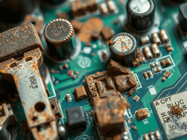
Masking And Keep-Out Areas
Before applying a coating, masking of connector, test, conductive, heat-transfer, switch, and service areas is necessary to protect them. A poorly made mask can allow the coating to be deposited on an area intended for clearance or contact and create a failure that looks electrical rather than mechanical.
Manual, Automated And Selective Coating
The method used for coating will depend on the complexity, volume, repeatability, and keep-out precision of the PCBA. Low-volume or small-batch work will typically involve using manual methods such as spray painting and brushing. Either process is capable of producing consistent coatings as long as the coating method remains the same for all assemblies of the same type. Ensure tight control over which areas do not get coated when using the dipping method, since during the dipping process, the entire board goes into the coating material at the same time. Automated spraying and selective coating improve consistency once a coating path repeats across many identical assemblies.
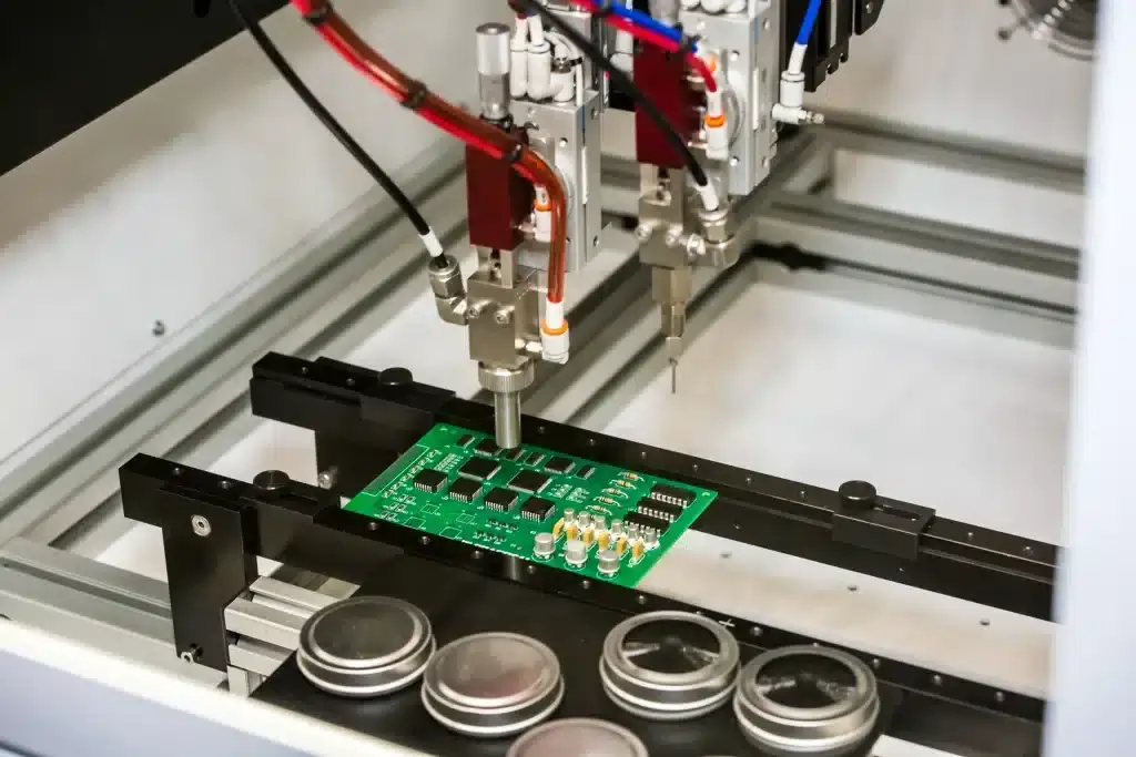
Curing And Rework
Different conformal coating materials cure in different ways. Acrylics can air dry, UV-curing systems require light to cure, some coatings require humidity-assisted curing, and heat-cured materials require that they be heated during curing, typically from 80°C to 110°C after an optional 60°C solvent flash-off period. Rework difficulty varies directly with how the conformal coating was cured. If curing used a solvent-reactivatable method like acrylic, rework is fairly easy. Conversely, with cross-linked methods like epoxy, rework has many more limitations.
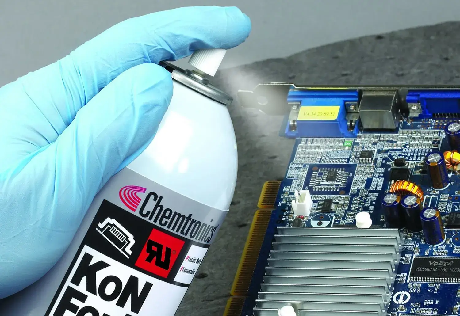
PCB Potting vs. Conformal Coating
Conformal coatings provide thinner, lighter assemblies that are easier to inspect and rework than potting. Potting typically provides much greater protective coverage and adds significantly greater weight, volume, and complexity when removal is necessary. The correct choice will depend on exposure conditions, vibration, how accessible the assembly is, and whether the assembly will require repair.
| Factor | Potting | Coating | Guidance |
|---|---|---|---|
| Coverage | Full encapsulation | Thin layer on board surface | Use coating when component visibility matters; use potting for enclosure-like protection |
| Best fit | Harsh environments, high vibration | Lightweight consumer electronics | For mixed assemblies, pot the high-risk zone and coat the rest |
| Moisture protection | Excellent | Moderate | Moderate resistance is not full immersion protection |
| Shock and vibration resistance | High | Low to moderate | If vibration is the main threat, mechanical support and potting matter more than coating alone |
| Rework | Difficult or impossible | Easy | Rework access is often the deciding factor when components need inspection or replacement |
| Weight and volume | High | Minimal | Weight-sensitive or compact assemblies usually favor coating unless risk requires encapsulation |
| Material cost | Higher | Lower | Cost should not override environmental risk, but it does change supplier and production planning |
| Common applications | Automotive, aerospace, industrial | IoT, telecom, wearables | These are starting points; exposure and rework still decide the final choice |
Choose Coating When Visibility Matters
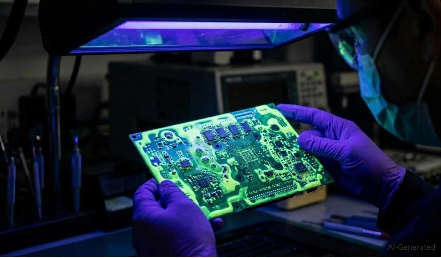
When an assembly requires moderate environmental protection but is also expected to be inspected, a conformal coating is the better solution. A thin conformal coating allows components to remain visible, adds minimal weight, and can be targeted to the specific areas of the assembly that require protection.
When Does Potting Fit Better?
Potting is the better solution when the assembly requires higher encapsulation protection, higher vibration resistance, tamper resistance, and conditions where future access is less important. The best indication that potting is preferable to conformal coating is not how much exposure it will see — rather, it is whether the assembly is designed to be serviced at all. A sealed, non-repairable module like a disposable sensor or single-use driver board can tolerate the disadvantages of potting because it will never need to be opened; however, a field-serviceable board may have thermal paths, connectors, or calibration points that must be accessed in the future.
Encapsulation Risks To Check
Before switching from conformal coating to potting, the following areas must be checked: thermal path, access to connectors, access to test points, the expectation of rework, and whether only a single localized area requires additional protection. A failure mode that can occur when using the two types of encapsulation is the bond where potting and a conformal coating meet. If the potting material does not bond well to the conformal coating, moisture may track along the interface of the two materials rather than through either material; the dam or mask line where they meet will require its own adhesion testing, in addition to visual inspection to verify both coating materials are present.
Inspection And Testing
When testing conformal coating, inspect where the conformal coating is located, where the areas without conformal coating are located, the thickness and adhesion of the conformal coating, and whether the environmental testing properly reflects the product's expected level of exposure. An inspection that gives a pass or fail answer is not enough; the inspection records must document what was inspected and against what specifications the inspection was conducted.
| Check | Purpose | Failure | Data | Record |
|---|---|---|---|---|
| Coating coverage | Coating is present only where required | Missing on protected zones, or present on no-coat zones | IPC acceptance criteria | Coverage note and visual/UV result |
| Electrical clearance | Foreign material does not violate minimum clearance | Leakage, short risk, contamination around lands | Minimum electrical clearance statement | Inspection finding with affected location |
| Edge coverage | Component and device edges are coated effectively | Thin edges, exposed corners, weak barrier | Component/device edge coverage target | Magnified visual check |
| Coating thickness | Thickness fits material and product targets | Too thin for protection, too thick for access/rework | 25-250 micrometers overall; 0.1mm-0.3mm for some bake-cured materials | Thickness measurement record |
| Adhesion | Coating bonds properly to the cleaned surface | Peeling, poor bonding, rework risk | Adhesion inspection statement | Adhesion check result |
| Visual and UV inspection | Coverage can be verified under light or UV | Hidden voids, inconsistent coverage | Visual and UV inspection criteria | UV image or inspection record |
| Environmental stress | Test plan matches actual exposure | Unvalidated humidity, salt spray, corrosion, or thermal cycling risk | Thermal cycling; humidity; salt spray; corrosion | Environmental test result |
| Standards use | Project standard is named and used correctly | Wrong standard claim or unclear acceptance criteria | IPC-CC-830C; IPC-A-610G; J-STD-001F; IPC-CC-830B; IPC-TR-587; UL94; UL746E; MIL-I-46058C | Standards list used for the check |
| SIR / dielectric | Coating does not create unacceptable charge transfer or insulation loss | Leakage risk on miniaturized or close-spacing boards | SIR; dielectric properties | SIR / dielectric test note |
IPC, UL And MIL Standards
IPC, UL, and MIL standards define the different elements of the requirement: IPC-CC-830C for the conformity and qualification of conformal coating materials, IPC-A-610G for workmanship on electronic assemblies, IPC J-STD-001F for the processes and materials used for the soldering of electrical and electronic assemblies, IPC-CC-830B as the previous qualification revision, IPC-TR-587 as the publication that describes how common thickness and coverage claims are established within the industry, and UL94, UL746E, or MIL-I-46058C as material or legacy requirements. Use the standards revision specified in the drawing or customer document.
Thickness, Adhesion And UV Inspection
To assess thickness on a conformal coating, a thickness range of 25 to 250 micrometers, or the separate 100 to 300 micrometers used for bake-cured material, should be used. The bake-cured material number is a separate spec for each individual material, and while it may run toward the upper end, it is a different spec than thickness measured under general guidelines. Treat these two numbers as separate references, then pair them with coverage, adhesion, and visual or UV inspection. If there is too little coating, the exposed areas of the substrate will remain unprotected; too much will inhibit access, affect cure rates, and complicate rework procedures.
Environmental Stress Testing
Environmental testing follows where the product is to be used; outdoor sensors usually stress validation for humidity and salt-fog, while miniature PCBs usually stress validation for SIR and dielectric performance. The -40°C to 85°C thermal cycling profile developed for a commercial part will not identify a failure mode that only occurs in the -40°C to 125°C temperature range for automotive use, so the test profile must reflect the actual performance specifications for the product instead of relying on a generic template.
PCB Design Before Coating
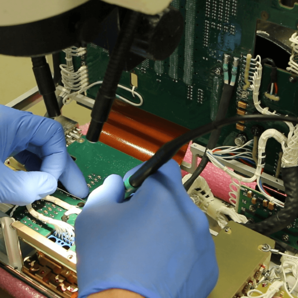
Before applying a conformal coating to a PCB, many issues related to coating application can be addressed through design considerations.
The following items show representative parameters used on PCBA coating lines. Verify the actual parameters used by the selected coating line before submitting the job.
| Design Check | Requirement | Risk If Missed |
|---|---|---|
| Handling rail | Technical rail at least 5mm | Board is hard to handle through assembly or coating |
| Board size window | 410mm x 410mm maximum, 10mm x 10mm minimum | Project needs a process check before it can run |
| Component height | 80mm maximum component height | Tall components block coating access or inspection |
| Keep-out spacing | 3mm shortest distance between coated and uncoated area | Overspray, contamination, unclear keep-out boundary |
| No-coat parts | Heat sinks, power resistors, power diodes, DIP switches, adjustable resistors, buzzers, battery/fuse/IC holders, tact switches — confirmed against the engineering no-coat list | Functional failure, impaired adjustment, poor heat release, or blocked service access |
| Surface cleanliness | Defined cleaning/plasma process specification | Weak bonding and poor adhesion |
| Thickness and bake | 0.1mm-0.3mm coating thickness; 60°C flash-off for 10-20 minutes before full cure | Wrong layer thickness or under-cure risk |
| Edge coverage | Coating must cover component/device edges | Exposed edges and local protection failure |
Design Areas That Need Keep-Out
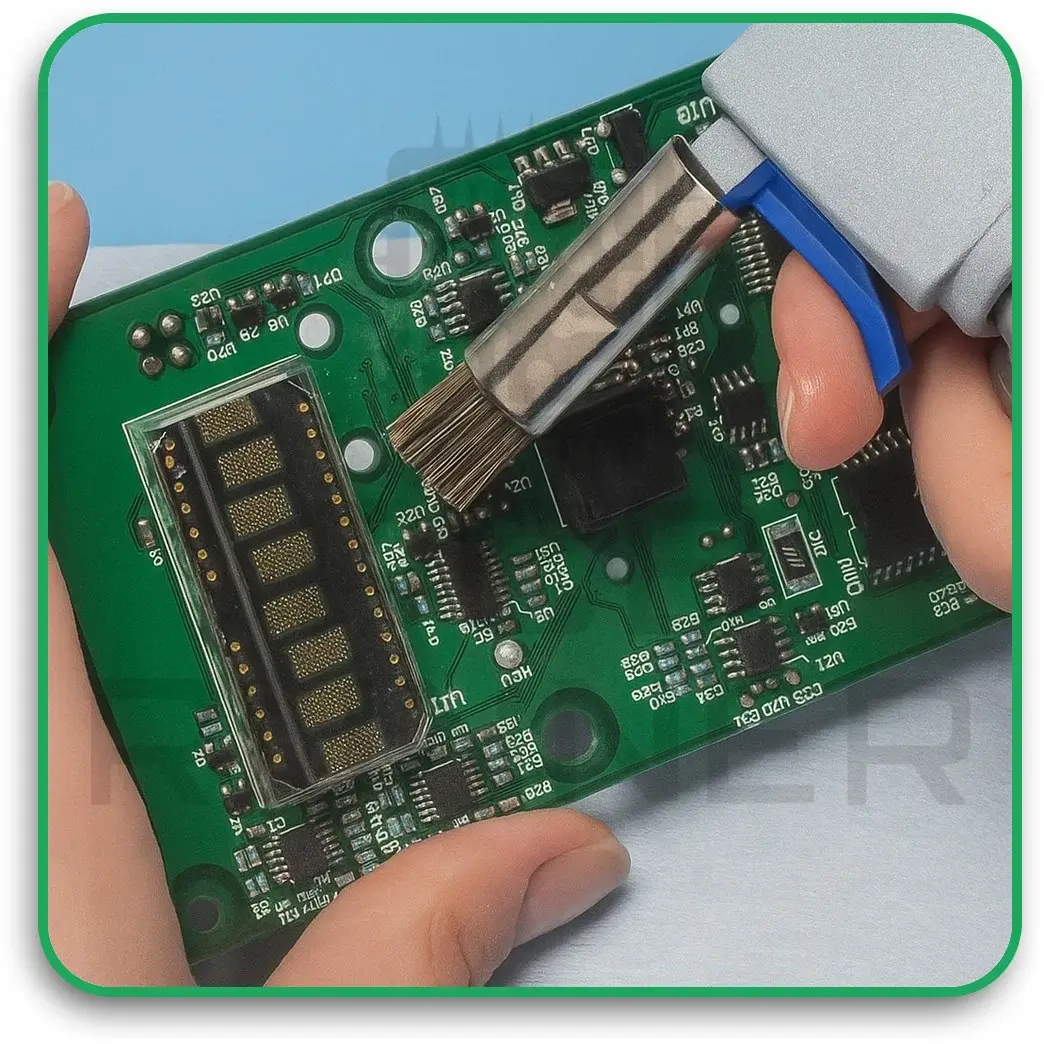
The keep-out areas must be clearly marked on the drawings before any masking. The coating operator needs no-coat areas and spacing between coated and uncoated areas identified on the PCB, so that there is no ambiguity regarding the location of keep-out areas. A minimum of 3mm between the no-coat area and coated area will provide an accurate, manageable boundary, as opposed to vague instructions to "avoid the connector."
Surface Cleanliness Before Coating
The cleanliness of the PCB is critical for successful adhesion of the conformal coating. Any contaminants on the PCB surface before the application of conformal coating will weaken the bond between the surface and the coating material. Absorbed material, including oil or moisture, will weaken the adhesion of the coating material.
Thickness And Edge Coverage Risks
Due to varying board designs, several factors contribute to the thickness of the conformal coating being applied. These factors include the geometry of the board, the height of components, and the amount of edge coverage on the device. A single average thickness will not be a reliable way of determining whether a conformal coating has been properly applied. To properly verify that the coating applied has sufficient thickness and is adequately covering the edge areas of the components, a microscope or magnifier is required.
PCB Applications
PCB applications are determined by failure modes and exposure conditions, including chemicals, liquids, gases, heat, moisture, salt fog, UV light, dust, vibration, corrosion, miniaturized spacing, or the need for a specific inspection method. If any of these items will affect long-term operation, then a conformal coating will need to be applied.
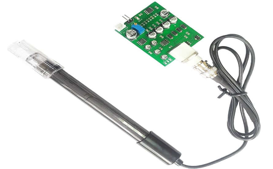
Automotive Sensor PCB
Automotive sensor PCBs typically experience extreme temperatures during operation, from -40 °C to 125 °C, as well as exposure to vibration, chemical substances, and road fluids. One of the most common mistakes with the coating for these boards is poor masking of connector backshells and machined ground pins. The presence of coating in connector cavities accounts for a significant number of product returns in the field, which causes OEMs to focus more on masking those areas than the overall board surface area. Acceptance for these PCBs is based on AEC-Q100-aligned qualification plans and environmental testing per ISO 16750, as opposed to simply filling out a generic salt-spray checklist.
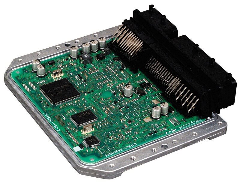
Vehicle Control And Power Electronics PCB
Concentrated heat develops around switching devices on vehicle control and power PCBs; this can be managed through selective conformal coating. Selective coating protects low-voltage components near the heat sources yet stops a few millimeters before the heatsink and power device body in order to avoid trapping excess heat against the component surfaces generating the heat. Acceptance criteria for thermal cycling and vibration testing of vehicle PCBs generally follow ISO 16750-4, or an OEM-specific equivalent test plan. Request a copy of this documented test plan from the supplier before assuming that a conformal coating will meet the acceptance criteria outlined in a standard validation.
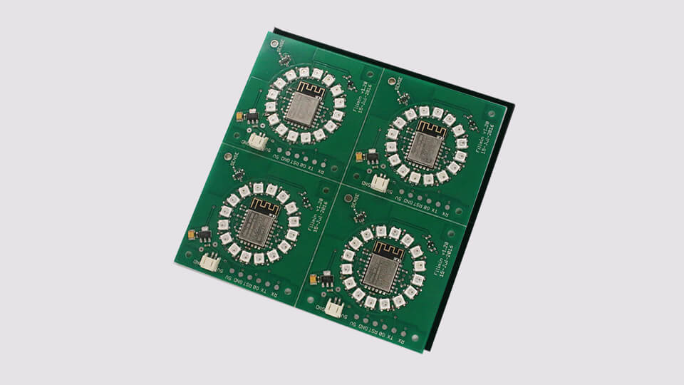
LED Lighting PCB
LED PCBs require a coating that is UV-stable and will not yellow over extended exposure to emitted light. Yellowing of the coating will alter color rendering, reduce lumen output, and cause degradation in the LED lighting application, even if the coating is still intact. Acrylic and UV-stable silicone materials are typical options here; testing for lumen maintenance through accelerated UV aging using an IES LM-80-style test is a stronger check than simply assuming any clear coating is optically neutral for an extended period.
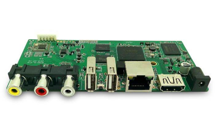
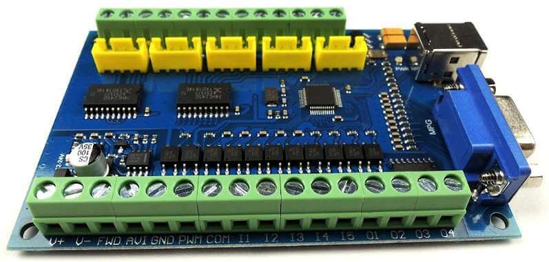
Consumer Appliance PCB
Moisture, cleaning agents, heat cycling, and household contaminants are all environmental elements that affect control boards found in consumer appliances. The most common coating omissions that lead to early failures in the field are front-panel membrane switches, rotary encoders, and adjustment potentiometers. In fact, the front panel usually has a greater number of failures than the main board itself. Many appliance programs still refer to safety clearances defined by IEC 60335-1 when determining if coatings should be used; compare the no-coat list with the safety clearance drawing, as they must be reviewed together, not independently.
Industrial Control PCB
Environmental conditions for industrial control boards include dust, chemical vapors, vibration, and temperature variations within the enclosure; condensation may occur on climate-controlled boards as a result of HVAC cycling. The coating decision should occur in conjunction with a review of cabinet door sealing, not as an isolated solution. Common testing methods, such as damp-heat cycling with IEC 60068-2-30 testing, are frequently used to verify the effects of condensation on boards before shipping, especially in cabinets that have experienced condensation issues.
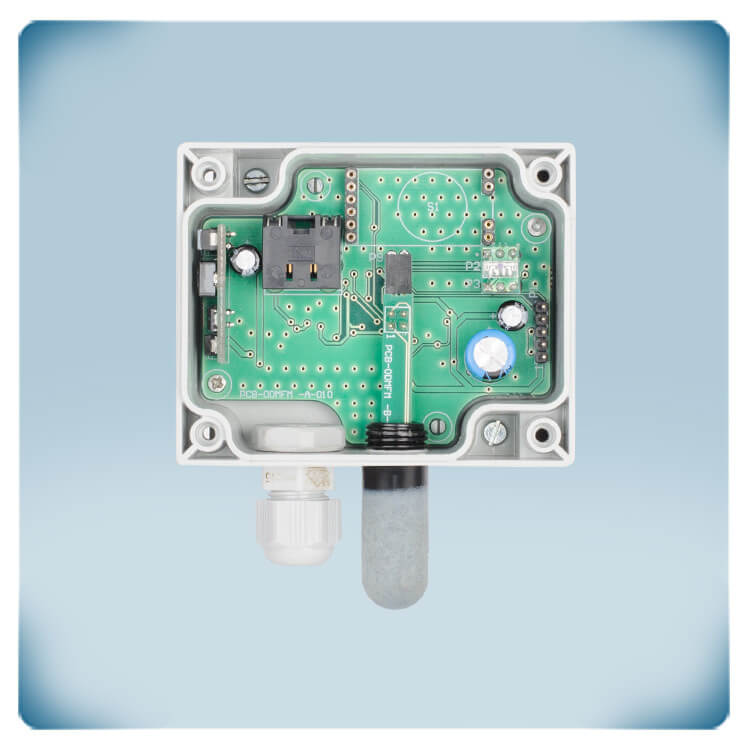
Outdoor Sensor PCB
Outdoor sensor boards need to be protected against condensation, humidity, salt spray, corrosion, and UV radiation within their enclosures. Coating and enclosure IP rating are complementary, not redundant. While poorly sealed enclosures may allow liquid water to pool on top of a coated board, the IEC 60529 ingress rating for the enclosure must be verified alongside the coating specification, not assumed from the outdoor product label.
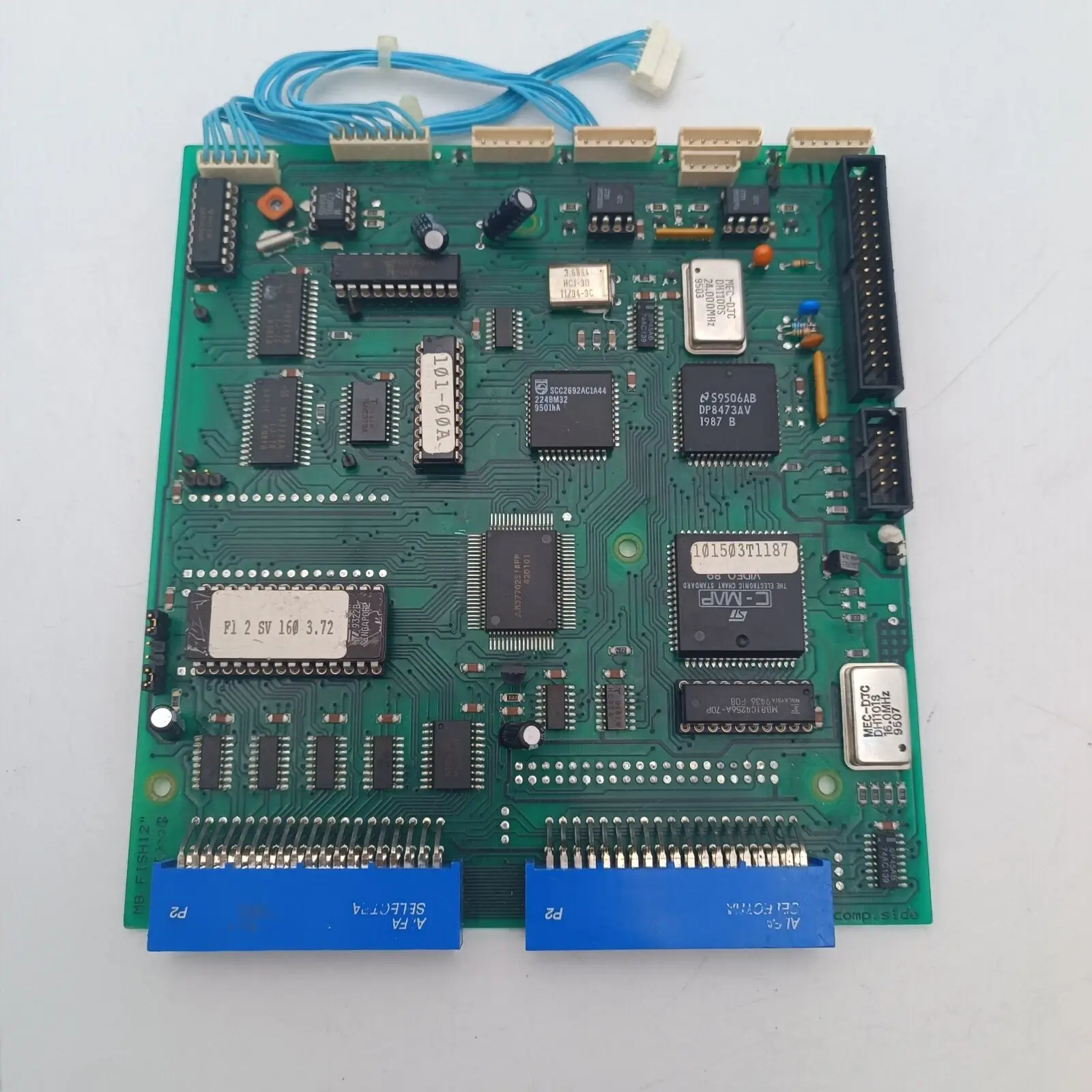
Marine And Navigation Electronics PCB
Marine and navigation electronics face fresh water vapor, salt fog, salty air, and corrosion. Connector backshells and battery terminals present the greatest risk for salt bridging. Coatings should ideally extend as deep into the connector backshell and battery terminal area as the design permits, and should be paired with salt-spray test results, which are regularly performed to the requirements established in ASTM B117 or the salt-mist section of IEC 60945 for marine navigation equipment.

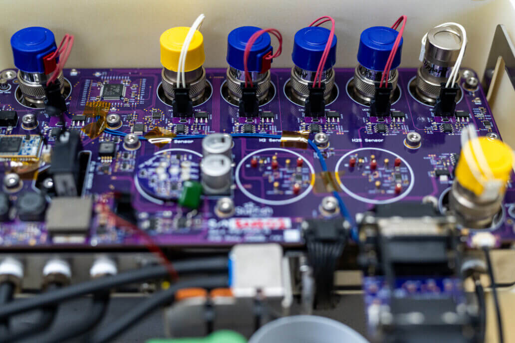
Aerospace And Avionics PCB
Aerospace and avionics PCBs experience pressure changes, dust, sand, moisture, and contact with various chemical compounds. Coating supports environmental qualification programs prescribed by DO-160-style testing, but it is one input into that qualification and should not be construed as a replacement for conducting the qualification test itself.
Medical Device PCB
In addition to surviving chemical wipe-downs with isopropyl alcohol and quaternary disinfectants during hospital cleaning, medical device PCBs must endure repeated exposure to these chemicals. Chemical resistance must be determined using data that reflects repeated chemical-contact exposure rather than a single chemical-resistance value. Implantable and biocompatibility-related work depends on the specific material grade and its associated ISO 10993 documentation, not on the coating family name. Request access to the biocompatibility file that corresponds with the material grade being quoted.
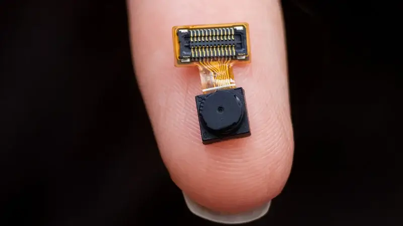
Miniaturized Electronics, MEMS And Lab-On-Chip PCB
Miniaturized electronics, MEMS, and lab-on-chip PCBs frequently use trace spacings of less than 0.2mm. Ionic residues left after processing change the insulation resistance of these types of PCBs far more than they would on traditional PCBs. When performing SIR testing using IPC-TM-650 methods, the results carry greater weight for Miniaturized Electronics, MEMS, And Lab-On-Chip PCB than for traditional consumer PCBs. Parylene's thin, uniform film coating is frequently the practical option despite its relatively high batch-processing cost.
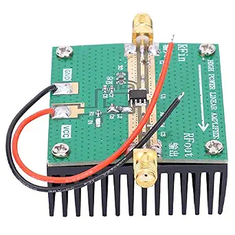
5G And RF Power Module PCB
Condensation, dust, temperature changes, and heat generated from RF power amplifiers and connectors affect 5G and RF power module PCBs, such as outdoor small-cell or macro base station units. Because dielectric constant and coating thickness can slightly shift impedance, 5G and RF power module PCBs with tight RF tolerances typically do not use coating in antenna and impedance-critical trace locations. Outdoor telecom enclosures of this type are typically qualified to ETSI EN 300 019 climate classes, which can serve as a useful starting point when determining the environmental range that the coating is going to have to support.
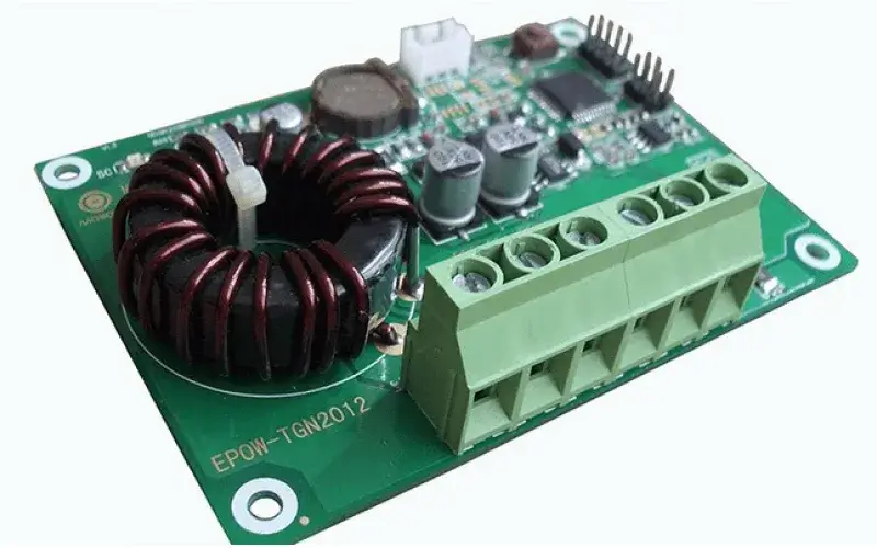
Solar And PV Inverter PCB
Control circuit boards for solar inverter and PV inverter applications experience rooftop temperature cycling, often a 40-60°C temperature differential between day and night, in addition to dust, UV radiation, and condensation from extended outdoor use. Applying a coating in conjunction with coated connector terminals helps address the predominant field failure mode for these applications: corrosion at the connector screw terminals as opposed to corrosion on the main PCB. Most manufacturers of inverters reference UL 1741 or IEC 62093 testing when establishing the environmental performance specifications of their application.
How To Choose A Conformal Coating Supplier
A conformal coating supplier needs clear material coverage, process control, masking capability, inspection records, standard alignment, volume support, and rework support.
| Question | Why It Matters | What To Check |
|---|---|---|
| Which materials can the supplier handle? | Material choice controls humidity, chemical, temperature, rework, and specialty fit | Acrylic, silicone, urethane, epoxy, parylene, and specialty coating experience |
| Which application methods are available? | Method changes consistency and keep-out accuracy | Manual spraying, automated spraying, selective coating, brushing, dipping |
| How are masking and no-coat zones controlled? | Coating contamination can cause operating failures | Keep-out approach, no-coat parts list, clearance handling |
| What inspection records are provided? | OEMs and quality teams need measured results, not coating claims alone | Thickness, adhesion, visual/UV inspection, environmental tests, SIR where needed |
| Which standards can the project use? | Standards must match the project, not act as generic badges | IPC-CC-830C, IPC-A-610G, J-STD-001F, IPC-CC-830B, IPC-TR-587, UL94, UL746E, MIL-I-46058C as applicable |
| Can the supplier support volume and rework needs? | Prototype, low, medium, and high volume carry different delivery risk | Volume tier supported; rework/removal approach |
| How are environmental and sustainability requirements handled? | Some projects need RoHS, lead-free, halogen-free, or low-VOC records | RoHS, lead-free, halogen-free, low-VOC; thermal cycling, humidity, salt-spray data |
| How does the supplier handle specialty or high-complexity coating? | Specialty materials or high-complexity coating need clear process capability | Deposition capability, masking control, inspection method, capacity plan |
| How should cost drivers be discussed before pricing? | Cost depends on material, method, quantity, coverage, thickness, and rework | Cost drivers by material and process variable |
Verifying Supplier Claims
A quality claim is only as useful as the paperwork behind it. Ask for the primary evidence instead of a summary statement: third-party lab SIR/dielectric test reports for the specific material and thickness used, cross-section photos or micrometer readings showing measured thickness against the target range, UV inspection photos or video from an actual production lot, and the coating material's current IPC-CC-830C certificate of conformance. A supplier that can produce these on request, tied to the actual lot or process date rather than a generic datasheet, is demonstrating process control rather than describing it.
Volume And Rework Support
Prototype, low-volume, medium-volume, and high-volume coating work stress different parts of the process. As volume rises, method choice, masking control, automated systems, inspection records, and rework/removal behavior all become more important to check before committing to a supplier.
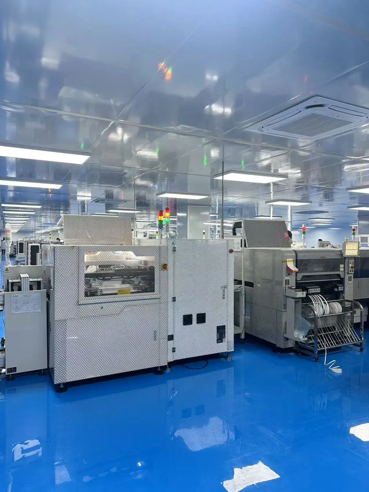
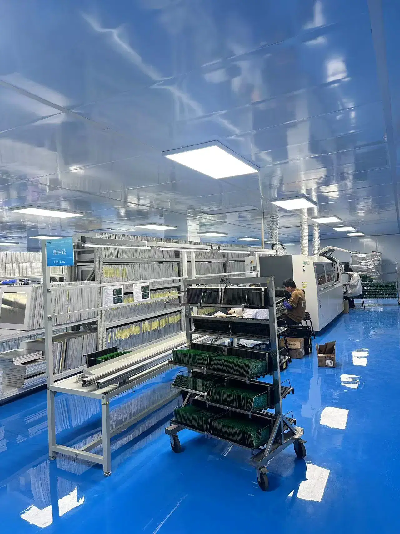
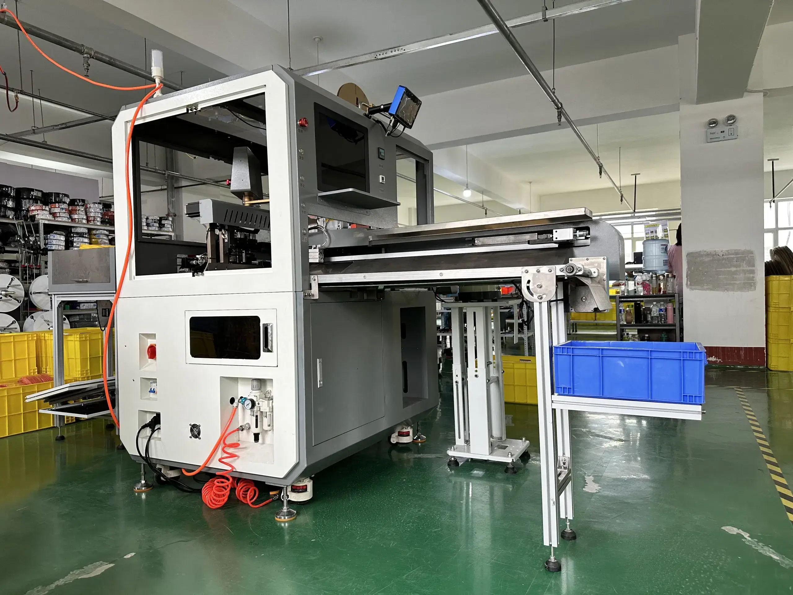
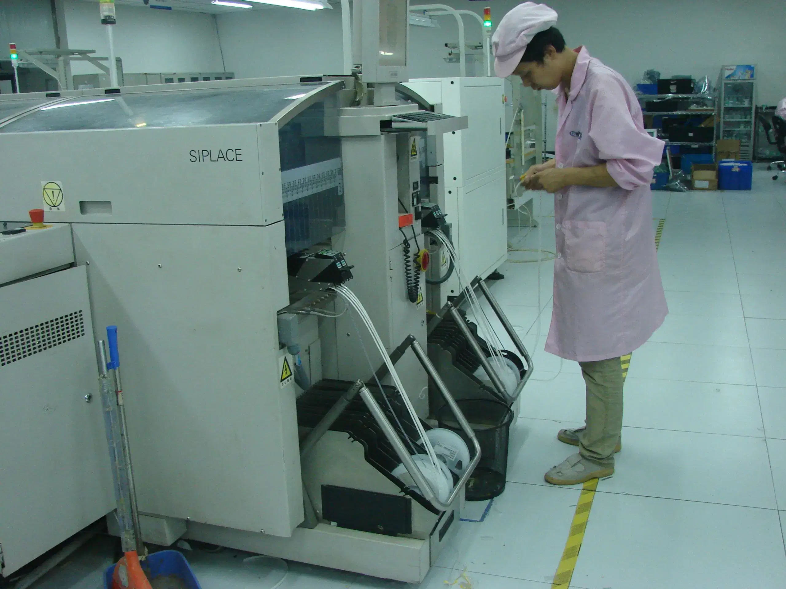
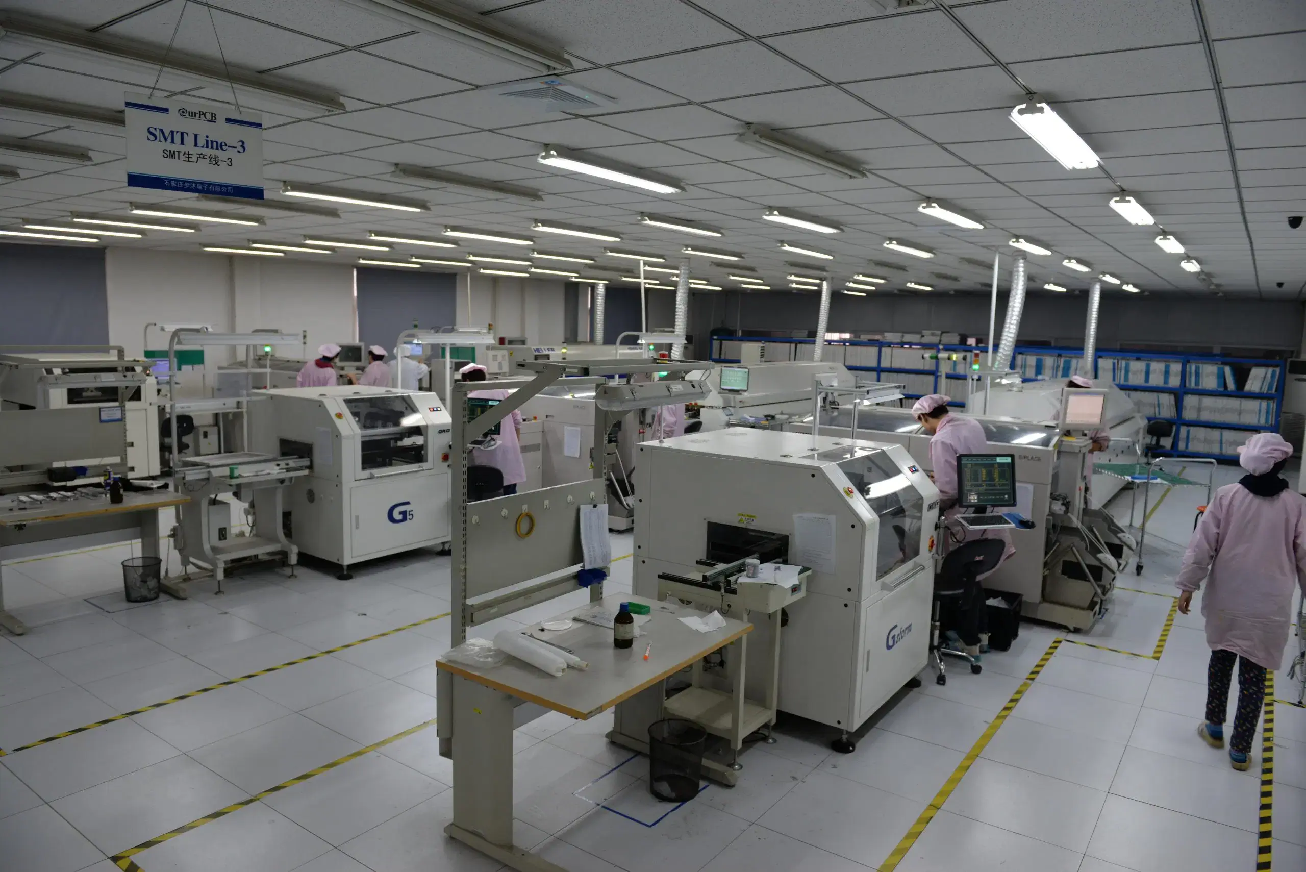
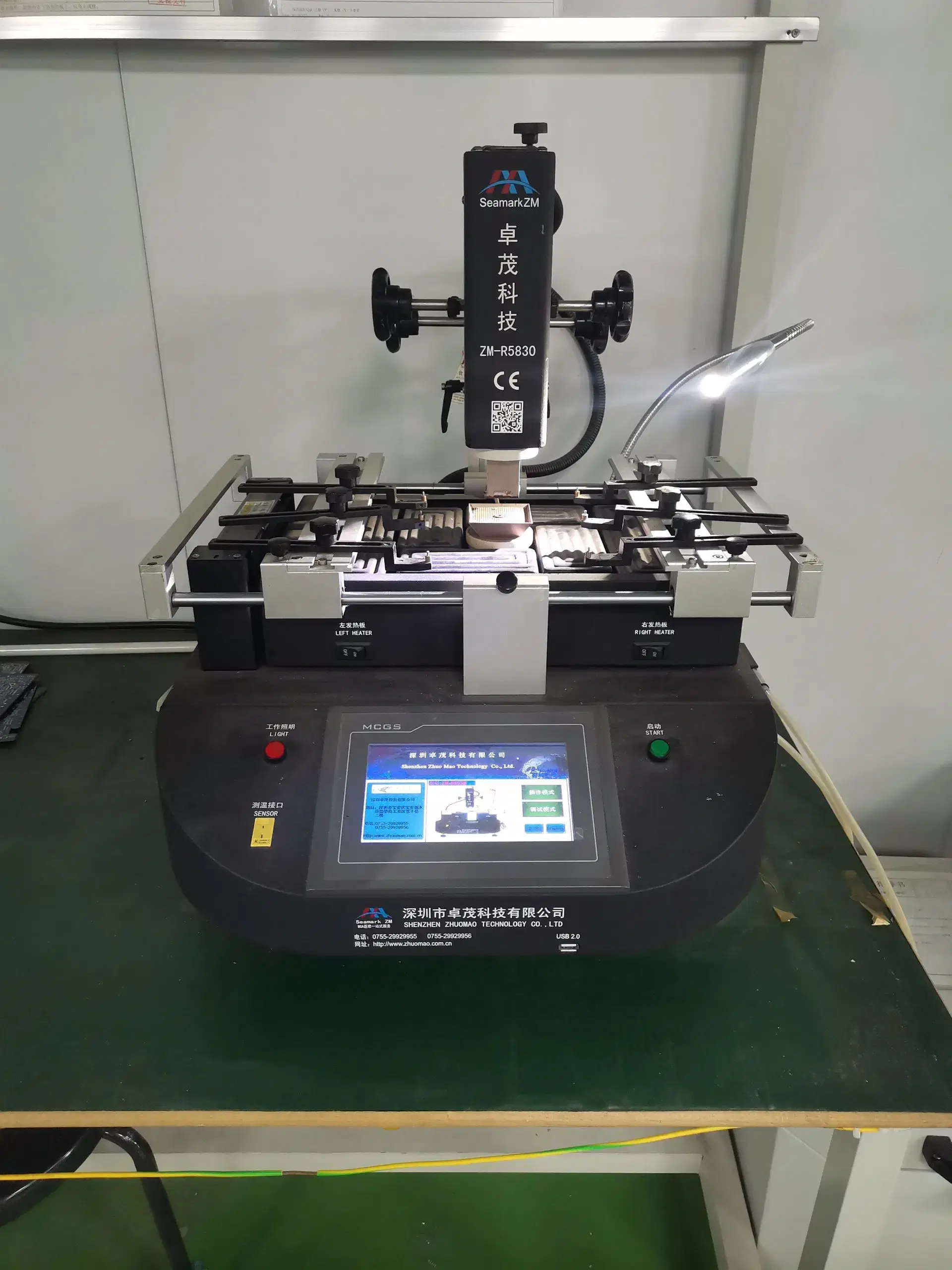
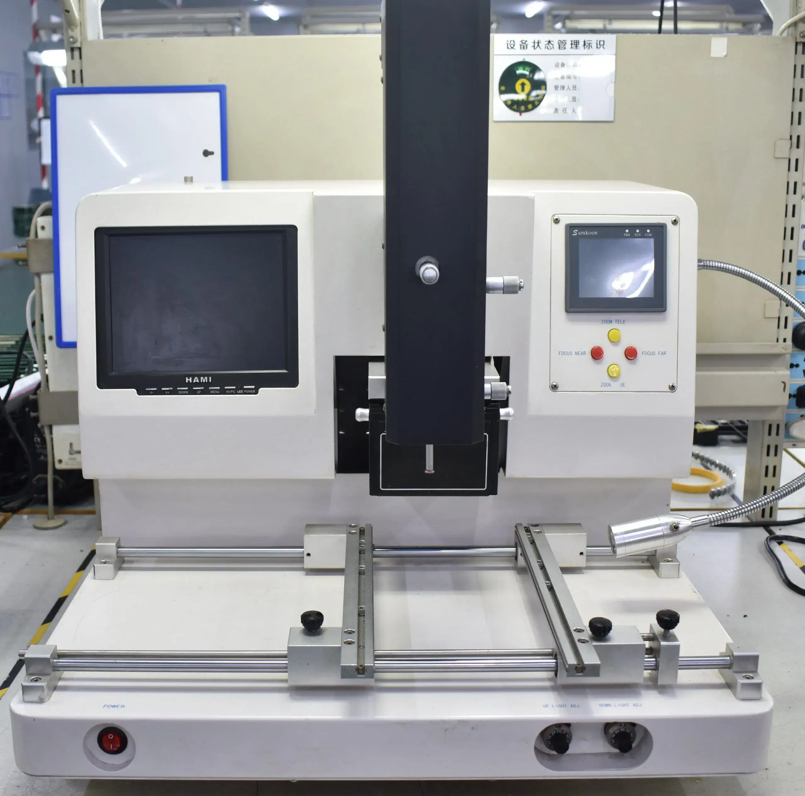
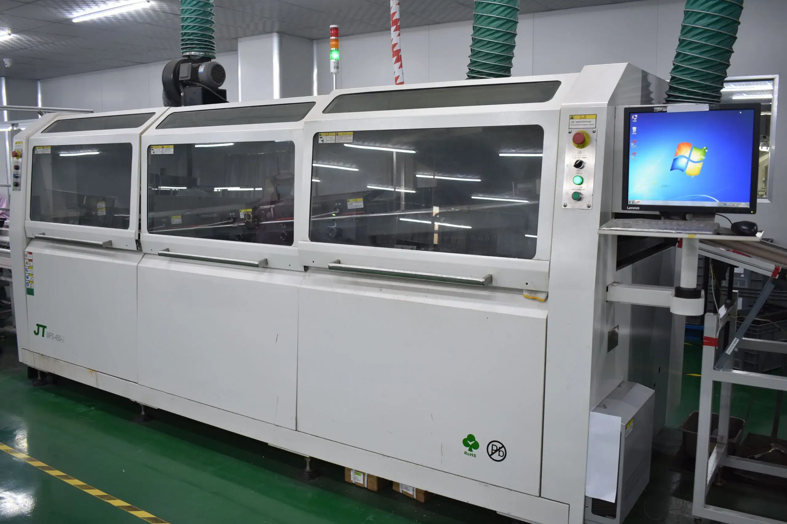
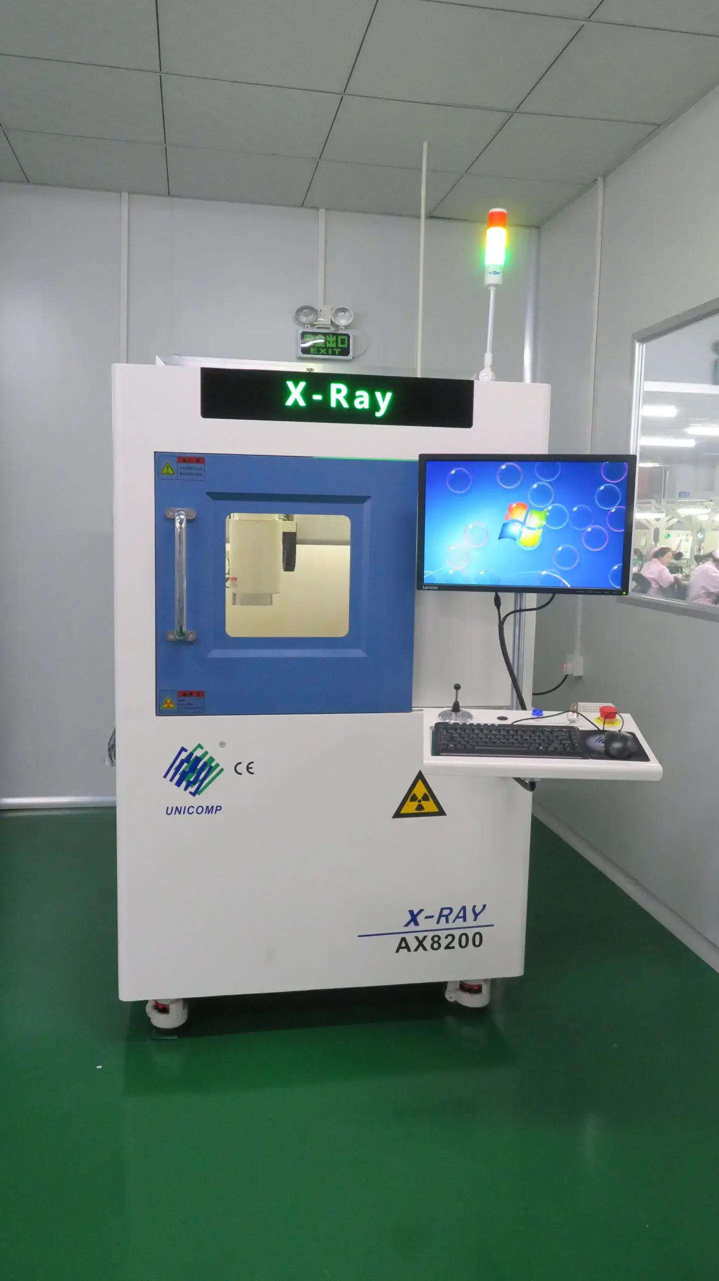
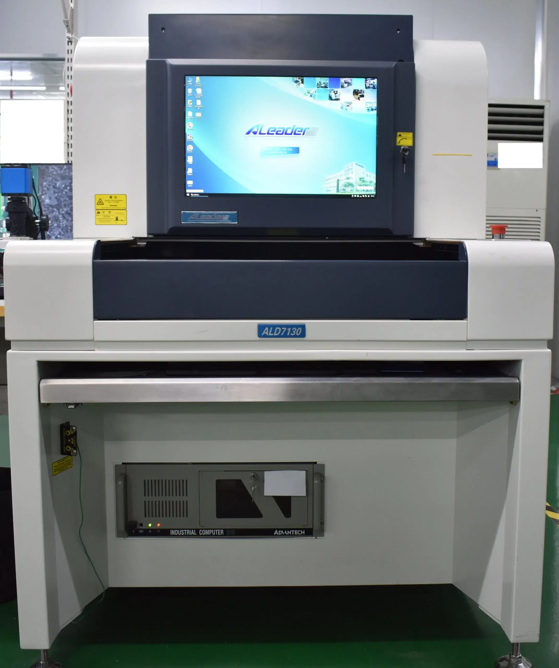
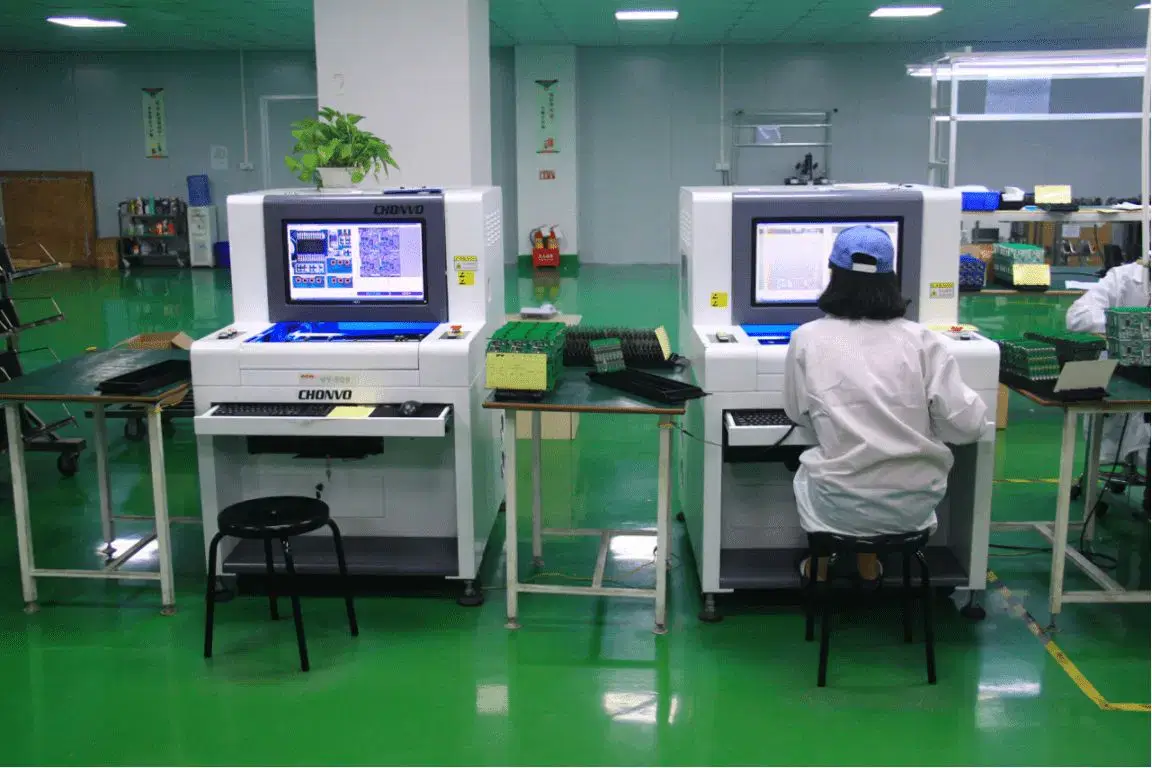
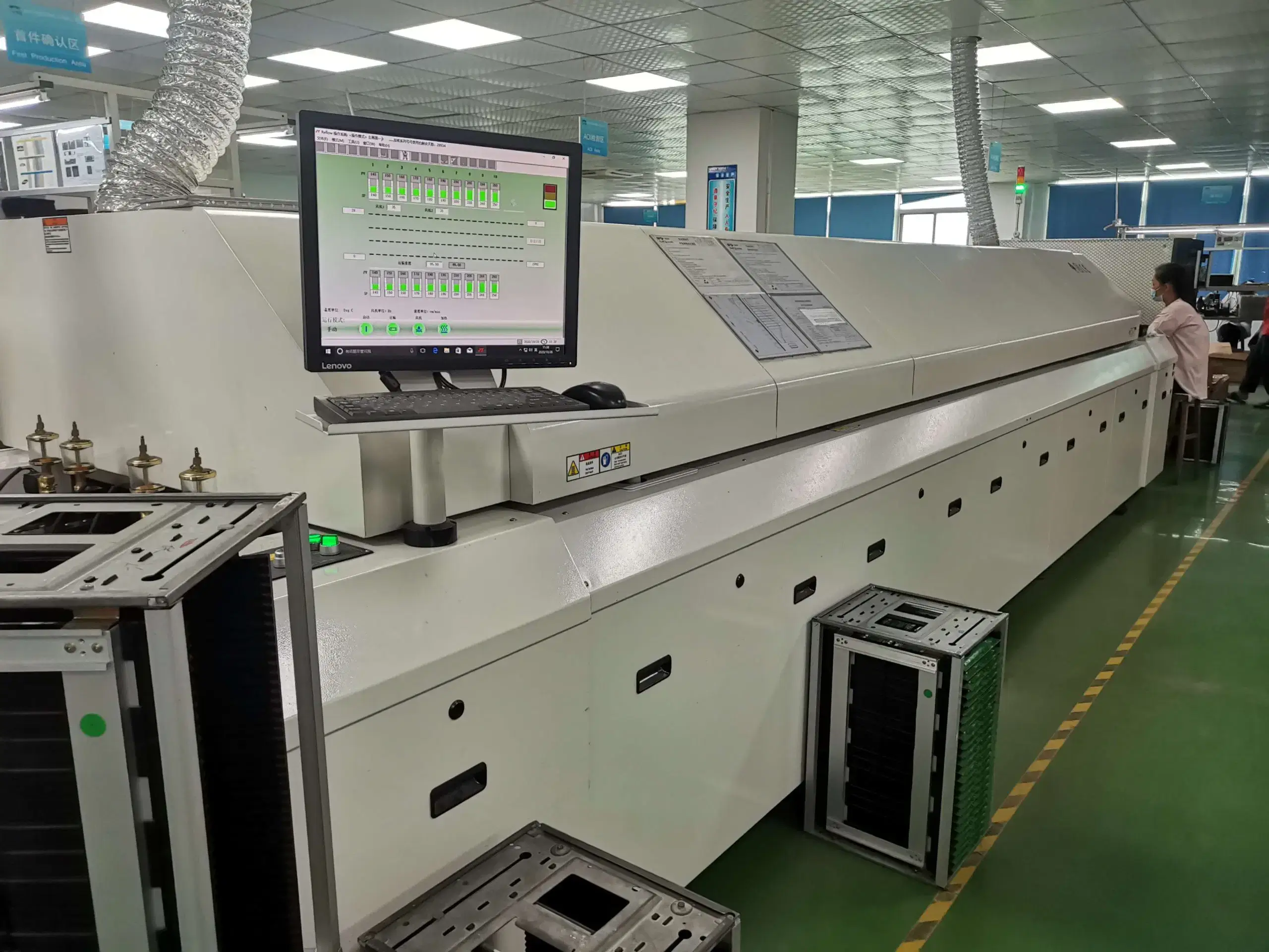
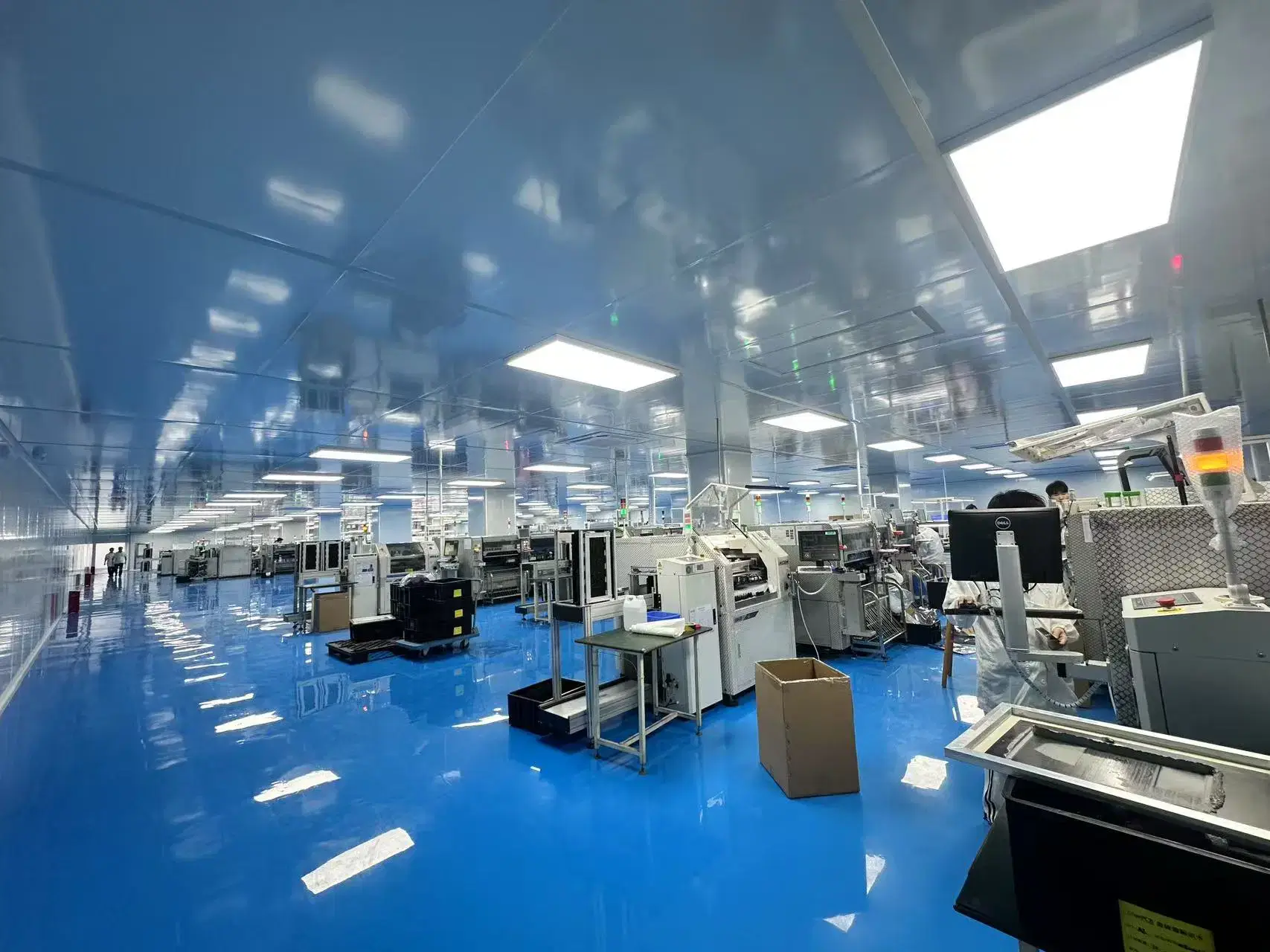
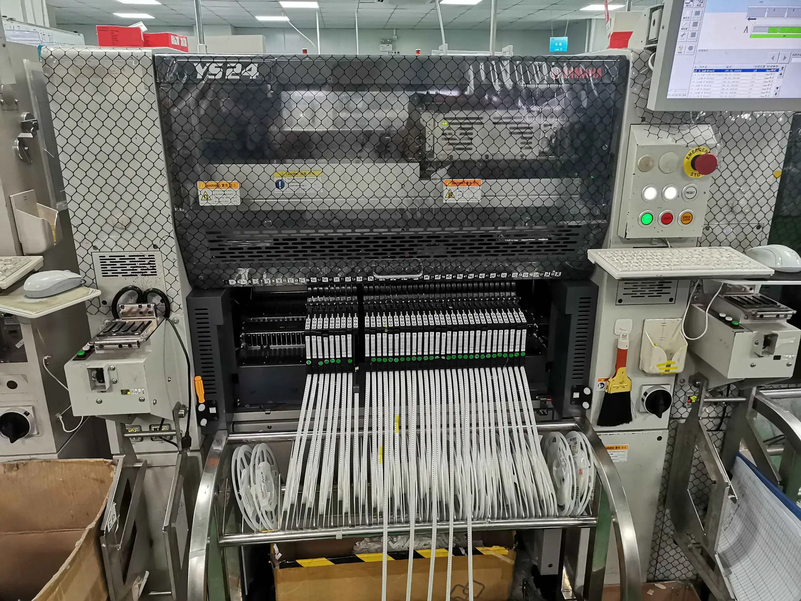
Our PCB Factory Gallery
Frequently Asked Questions
No. Conformal coating is useful when PCB assemblies face moisture, dust, chemicals, temperature variation, leakage risk, corrosion, or contamination. An indoor, low-risk PCB inside a controlled enclosure may not need it.
The main disadvantages are material mismatch, masking mistakes, extra rework effort, added inspection needs, partial moisture protection, and no-coat zones around connectors or service parts. In severe shock, immersion, or tamper-resistant designs, potting or enclosure protection fits better.
No. At the typical 25-250 micrometer film thickness, conformal coating improves resistance to humidity, condensation, and salt-spray-related risk, but it does not protect against full immersion or sustained water pressure the way a sealed enclosure does.
For sustained exposure above roughly 85% RH, silicone or parylene generally hold up best across a wide temperature range. If the board also needs to be field-reworked, silicone’s flexibility makes a local cut-and-patch repair realistic; parylene typically needs the affected area fully recoated rather than spot-repaired. Acrylic covers moderate humidity with the easiest rework, and urethane adds chemical and abrasion resistance alongside humidity protection when the exposure includes solvents or abrasive contact, beyond moisture.