Upload BOM & Gerber
-
Mobile: +86 13312967631
-
Email: sales@sugaintl.com

PCB & PCBA Quality Inspection Services
PCB Inspection at Every Production Stage
SUGA inspects printed-board condition, solder-paste deposition, component placement, visible assembly workmanship, hidden solder structures, and first-article conformity at the production stage where each feature can be observed or measured.
30+ Years Electronics Bare PCB + PCBA Manufacturing
SPI · AOI · X-Ray · FAI · Visual
Prototype through high-volume production
Solder paste, placement, hidden solder, and first-article coverage
What Is PCB Inspection?
PCB inspection involves evaluating a bare PCB or a PCBA according to requirements that define the physical characteristics specified by the manufacturer or customer. Each area of coverage is determined based on when a specific feature will be visible or measurable; therefore, the inspection target may include the incoming board, printed solder paste, component placement, the reflowed assembly, hidden solder structures, or the first completed article. Findings from each PCB or PCBA inspection are associated with the following attributes for each board or lot: the board or lot number, the location of the finding, the criterion, the initial result, the action taken, and the status of the follow-up inspection.
PCB and PCBA Inspection Coverage
For example, incoming PCB inspection assesses visible external characteristics such as outline and hole features, solder mask, legend, exposed copper, accessible plated areas, markings, distortion, contamination, and handling damage. Internal copper thickness, dielectric construction, buried features, and the integrity of internal plated vias cannot be determined through visual inspection of the top or bottom surfaces of the bare board. Therefore, when the project requires inspection of these internal features, acceptance also uses approved fabrication data, electrical test records, material certifications, coupons or microsections, and specified plating measurements generated in accordance with the applicable printed-board criteria.
In contrast, PCBA inspection assesses solder-paste printing, component placement, the reflowed assembly, hidden solder structures, first-article confirmation, and final workmanship. The five different PCB inspection services discussed below pertain only to PCB assembly, while bare PCB acceptance remains governed by the approved fabrication data, incoming requirements, and applicable printed-board criteria.
PCB Inspection vs. PCB Testing
Inspection and testing answer different questions. PCB inspection determines whether observable or measurable manufacturing features conform to the approved criteria. It identifies paste variation, missing or misaligned components, visible solder concerns, hidden-joint image signals, board damage, and configuration differences.
Testing determines whether an electrical or functional response meets its requirements. A board can meet visible workmanship requirements and still require electrical or functional testing. Optical and X-ray results describe manufacturing conditions rather than circuit behavior.

Why Early Inspection Matters
Why Does Early Defect Detection Reduce Cost?
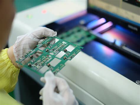
If a defect is found early while the feature of interest remains accessible, a team has a greater ability to contain it before further operations add value. A solder-paste variation before placement can be linked directly to the conditions under which the paste was printed. A placement error observed before reflow can be corrected without treating it as a completed solder-joint problem. Once the feature is blocked from view by a shield, a tall component, a later assembly step, or a finished product, the same error may require disassembly, rework, or additional inspection.
In addition, the later a defect or discrepancy is discovered in the manufacturing process, the greater the impact on traceability. Engineers may need to evaluate the defect or discrepancy not only in relation to a single board or process interval but also across the panels, lots, materials, programs, or revisions exposed to it.
How Do Inspection Results Support Acceptance and Escalation Decisions?
Following inspection, the results support an acceptance or escalation decision based on what was inspected, the criteria used to evaluate the results, and whether the findings were confirmed through measurement, visually confirmed, or unresolved because of limited access.
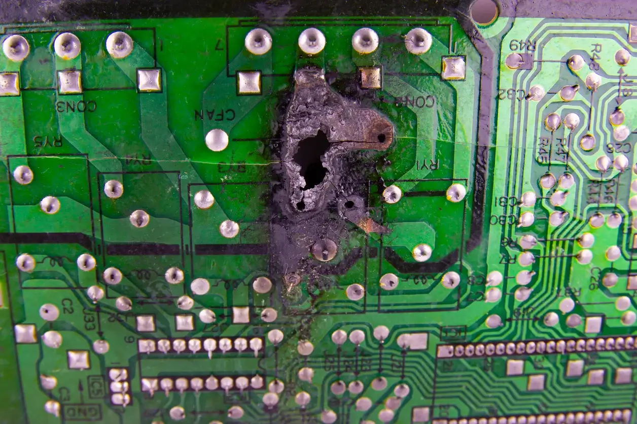
A confirmed inspection result related to paste, placement, solder, board, or handling can trigger correction, reinspection, examination of related units, or process escalation. Acceptance of an inspection result does not confirm the service life of the product. Instead, it documents the manufacturing condition that the selected inspection method was able to resolve.
Defects by Visibility and Failure Mode
When reviewing defect visibility and failure modes, a defect is evaluated based on what the inspection method can resolve, the associated manufacturing consequences, and whether the same defect signal appears repeatedly at a stencil aperture, board location, panel position, or lot.
| Defect Category | Inspection Signal | Manufacturing Risk | Follow-Up Method |
|---|---|---|---|
| Solder Paste / Printing | Low or high deposit; height/area/volume deviation; bridge; tail; shape variation; offset | Open or short; solder imbalance; placement instability; recurring post-reflow defects | 3D SPI; aperture/location analysis; print correction; post-reflow confirmation |
| Visible Assembly | Missing/misaligned part; polarity error; lift/tilt; solder variation; pad damage; contamination; burn mark | Assembly nonconformance; weak connection; rework; recurring placement or solder defects | Visual or magnified inspection; 2D/3D AOI; correction reinspection |
| Hidden Interconnect | BGA/QFN/CSP void, bridge, low solder, alignment variation, head-in-pillow/non-wetting indicator; PTH fill variation | Latent interconnect weakness; localized thermal resistance; intermittency; hidden nonconformance | Targeted 2D/2.5D/3D X-ray; criteria comparison; alternate view when required |
| Board / Connector / Mechanical | Warpage; crack; bent/missing pin; insertion/coplanarity variation; housing or edge damage; handling mark | Contact instability; solder stress; assembly interference; handling damage; integration risk | Multi-angle visual; magnification; 3D AOI geometry; first-article comparison; reinspection |
Solder Paste Defects
Solder paste defects are easily detectable immediately after the paste is printed onto the board. An isolated low or high deposit may be indicative of local contamination, a problem with the support for the printed circuit board, or one specific release event. When the low or high deposits are repeated at the same aperture, this may indicate issues such as the stencil opening, the length of time since the last cleaning, paste release consistency, or print alignment. If the repeated deposits are located at a single position on the panel, this could indicate an issue with the support for that area or possible warpage of the printed circuit board.
Once a corrective action is approved, the next print is measured at the same location, and the corresponding post-reflow solder joint is checked; however, an acceptable SPI result does not guarantee that the completed solder joint is acceptable.
Visible Assembly Defects
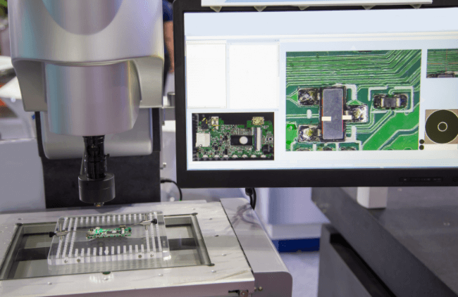
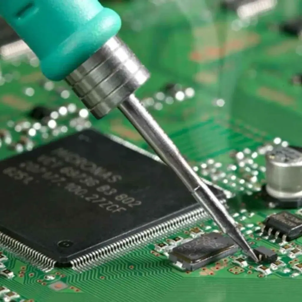
Magnified visual inspection can help clarify local surface conditions, while 3D AOI can help provide height and geometrical measurements.
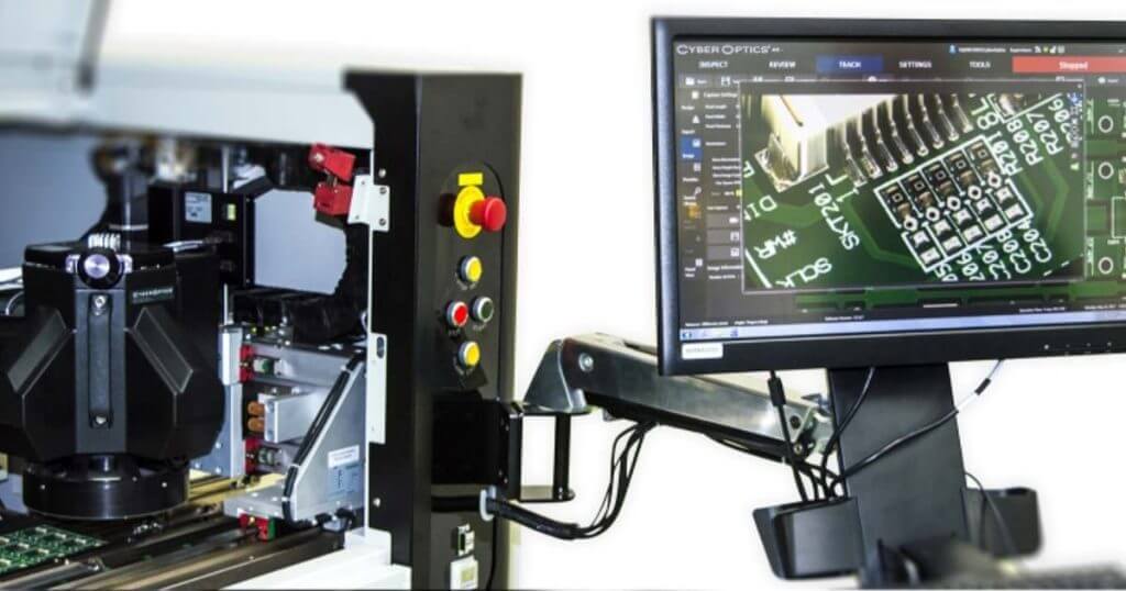
In addition to the difficulties with detecting defects caused by reflection, shadowing, and dense layouts, there are also complications with the use of AOI due to similar packages and outdated references.
A magnified image is not in itself sufficient to determine a final disposition. A component may still have incorrect polarity, seating, lead condition, package marking, or solder joint geometry. The determination of whether a call is valid will be made using controlled lighting, an alternate view, or magnification; approved substitute components will be verified with reference to the released BOM and assembly data rather than solely through visual outline comparison.
Hidden Solder Defects
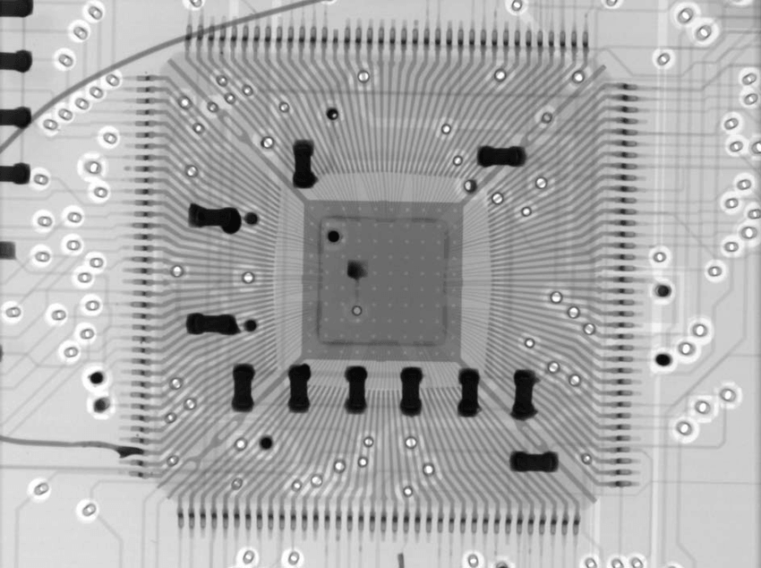
Solder structures located beneath a package are hidden from optical inspection and therefore must be inspected by X-ray, since optical methods cannot see beneath the package. The configuration of the X-ray system will depend on the type of package being inspected, the density of components on the printed circuit board, the amount of copper overlap, and the presence of additional components on the opposite side of the printed circuit board. The purpose of the inspection will also affect the X-ray configuration; for example, the areas of interest may include suspected voiding, bridging, alignment, PTH fill, or suspected interface separation.
A 2D top-down image may show a void or bridge, but some areas may still not be visible. Oblique or 3D imaging, comparison with adjacent joints, and consistent settings help separate a local defect from normal package overlap or artifacts seen when using X-ray. SUGA is capable of configuring X-ray systems up to 160 kV and using oblique views up to 82° when penetration or structure separation requires it. The actual configuration of the X-ray system will be determined based on the type of package being inspected, its construction, the construction of the printed circuit board, and the resolution required for inspection. Head-in-pillow and non-wetting remain indicators when the joining interface cannot be fully separated during X-ray inspection.
When Does Physical Damage Require Engineering Escalation?
Engineering escalation occurs when the depth, repetition, or relationship of physical damage cannot be determined through routine workmanship inspection techniques. Physical damage is then evaluated based on its relationship to connector interfaces, mounting points, flex transitions, plated features, insulation gaps, or areas that carry electrical current.
Engineering verification uses information obtained through multiple viewing perspectives and associated magnification, as well as geometry measurements and comparisons with the approved first article, to determine whether to accept, correct, reinspect, isolate affected units, or request another evaluation.
Although physical damage and visible marks may appear limited, they can affect component fit, contact pressure, solder attachment stress, insulation distance, or future handling; therefore, the record should separate cosmetic evidence from damage that may affect assembly or integration.
Inspection Method Selection
No single inspection method will cover all areas of the production process. Selection of the correct inspection method is based on when the target remains accessible, which inspection method can resolve the signal, and whether the anticipated output will satisfy the acceptance criteria for the assembly.
| Inspection Method | Production Point | Inspection Target | Required Output | Physical Limitation |
|---|---|---|---|---|
| Visual Inspection | Incoming; first article; in-process; final; post-rework | Board condition; markings; presence/polarity; exposed pins and solder; contamination; damage | Observation or image; feature location; approved-reference comparison | Optical access only; hidden joints require X-ray |
| 3D Solder Paste Inspection | Post-print; before placement/reflow | Paste height, area, volume, shape, bridge risk, tailing, offset | Measured geometry; board/panel location; trend feedback | Paste deposition only; not completed-joint condition |
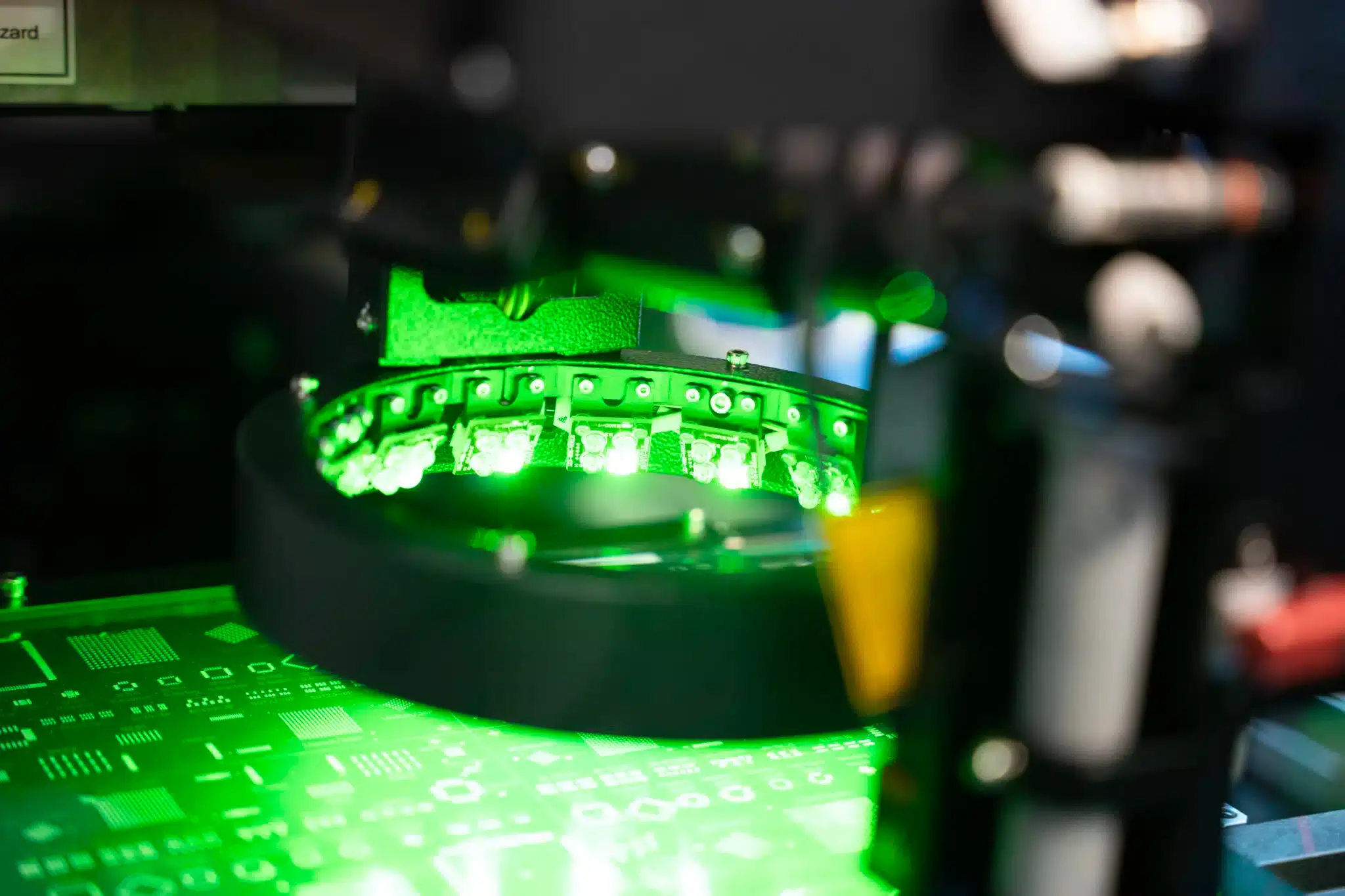
| 2D/3D Automated Optical Inspection | Post-placement; post-reflow; selected in-process points | Presence; polarity; X/Y/rotation; height/lift/tilt; leads; pads; visible solder geometry | Repeatable image; dimensional result; confirmed call; lot trend | Limited by access, shadow, reflectivity, geometry, and program/reference quality |
| X-Ray Inspection | Post-assembly; optically inaccessible solder/structure | BGA/QFN/CSP joints; void; bridge; insufficient solder; alignment; PTH fill; interface-separation indication | Internal image; measured or classified indication; location; criteria comparison; reinspection result | Resolution depends on overlap, package, board construction, angle, and configuration |
Which Inspection Method Applies at Each Production Stage?
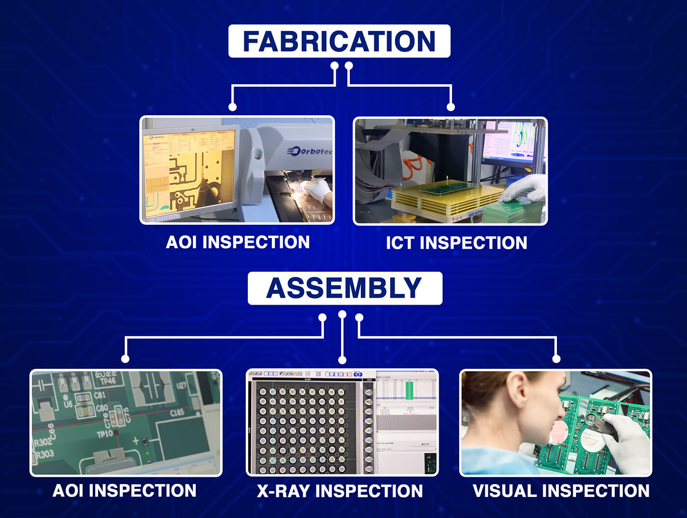
The inspection plan defines access closures related to shields, tall connectors, light glare, shadowing, or other overlapping structures that may block the view of the target during production. The critical locations of the target are assigned a production point, inspection method, acceptance criterion, and required image or measurement.
When it is impossible to use the chosen inspection method to verify one or more requirements, the gap is noted, and another method, a different inspection point, or an alternate view is assigned. An unobserved characteristic will not be accepted as passed.
When Should AOI and X-Ray Be Combined?
When an assembly contains both visible surface features and hidden solder joints, AOI and X-ray will be used in combination to determine whether the assembly will be accepted. AOI will cover the accessible placement of the package, surrounding components, leads, and visible solder geometry, while X-ray will inspect the joints on the underside and any other hidden parts of the assembly.
The combination of the two inspection methods will be planned according to the feature and not the circuit board-level label. For example, a BGA may require X-ray inspection of the underside joints, while neighbouring polarity markings, leads, or exposed solder are inspected visually or with AOI. An AOI pass does not guarantee the status of an underside joint, and an X-ray pass does not guarantee the status of any neighbouring markings or exposed leads. Both AOI and X-ray inspection results will be retained instead of allowing one method to substitute for the other.
Standards for Product Acceptance
PCB inspection standards apply to specific types of inspection objects. They do not replace the product drawing, procurement specification, contract, customer requirements, approved deviations, or selected Product Class for the products being built. Each inspection setup document and the corresponding report will identify which standard revision was assigned to a job so that any future updates to the documentation will not change the basis of the original decision.
| Engineering Field | IPC-A-600M | IPC J-STD-001J | IPC-A-610J |
|---|---|---|---|
| Inspection Object | Printed board | Soldered assembly materials and process | Completed electronic assembly |
| Control Role | Bare-board fabrication/incoming acceptance | Soldering and assembly process requirements | Post-assembly workmanship acceptance |
| Evidence | Accessible board condition; dimensions; holes; external conductors/spacing; accessible plating; documented material/structure evidence | Process records; material and hardware controls; soldering requirements; inspection results | Mounting; leads; terminations; solder connections; board condition |
| Production Point | Before assembly / incoming board verification | Assembly planning, execution, inspection, confirmation | First article, in-process, final, incoming, post-rework |
| Required Project Data | Class; drawing; procurement specification; customer requirements; deviations | Class; assembly drawing; process requirements; customer requirements; deviations | Class; drawing; contract; customer requirements; deviations |
IPC-A-600M for Printed Boards
The purpose of IPC-A-600M is to provide criteria for the acceptability of printed boards that relate specifically to printed boards and not to final assembly workmanship. While incoming visual or dimensional inspection can verify the external condition of each printed board, the specified records, coupons, microsections, or measurement evidence are required to validate the internal construction and plating of each printed board. Acceptability is based on the released fabrication drawings, procurement specifications, assigned Product Class, and approved deviations.
IPC J-STD-001J for Soldered Assemblies
IPC J-STD-001J provides specifications for soldering materials, soldering processes, cleanliness, hardware installation, and soldered connections. IPC J-STD-001J describes the process requirements used to produce soldered connections, unlike IPC-A-610J, which provides the criteria that the completed solder joint must meet. Although the joint may meet the requirements of IPC-A-610J visually, the joint may not have been produced by following the process required by IPC J-STD-001J. The contract, customer documentation, and process controls assigned to each assembly determine what records and inspection outputs are required for an assembly. The standard is not intended to be a complete report-management process.
IPC-A-610J for Electronic Assemblies
IPC-A-610J contains the criteria for the acceptability of completed assemblies regarding how the parts are mounted, the leads and terminations of the parts, the visible solder joint connections, and the overall condition of the printed circuit board. Thus, IPC-A-610J can be used for first-article, in-process, final, and post-rework evaluations of the completed assembly. The customer procedure or quality plan will define how far the FAI must go and the sequence in which it must be released. The criteria for accepting a concealed joint belong to the inspection method assigned to the feature outside optical accessibility.
Which Product Class Applies?
Product class comes from the governing contract and product documentation, not from industry name, board appearance, or production volume.
The inspection record identifies the governing documents, their revisions, feature-specific requirements, and approved exceptions. Conflicts or unclear criteria need resolution before the affected feature is accepted.
Inspection Process and First Article Control
| Production Point | Engineering Inputs | Inspection Focus | Required Output |
|---|---|---|---|
| Inspection Setup | Gerber/ODB++ or fabrication data; assembly drawing; BOM; placement data; reference; class; customer requirements; critical features | Revision; inspection object; timing; coverage; viewing or image condition; measurable and inaccessible features | Coverage definition; criteria; feature list; method assignment |
| Solder Paste Inspection | Printed board; stencil/paste data; print reference; board support; panel ID | Paste geometry; repeated aperture/location/panel pattern | Measurement; correction; following-print confirmation; trend feedback |
| Placement / Pre-Reflow | BOM; centroid data; polarity data; feeder/program reference; first placed board | Presence; orientation; polarity; position; lift/tilt; placement condition | Image/measurement; correction result; reflow approval |
| Post-Reflow Surface | Reflowed assembly; AOI reference; visual criteria; process lot | Visible components/solder; contamination; markings; board/mechanical condition | Pass; confirmed call; correction; additional inspection; reinspection |
| Hidden-Feature Inspection | Package/board construction; hidden-feature list; X-ray configuration; acceptance requirements | Hidden joints; obscured solder; PTH fill; alignment; interface-separation indications | Internal image result; criteria comparison; reinspection |
| First Article Inspection | Approved product data; first assembly; process settings; material traceability; inspection results; deviations | Configuration conformity; required stage results before production release | FAI result; deviations; corrections; release or approved disposition |
| Inspection Findings / Process Feedback | Inspection/repair records; lot/process data; repeated signals; correction instruction | Containment; correction; reinspection; process correlation | Final result; affected quantity; lot/process link; corrective-action reference |
Inspection Setup
Before production, the Inspection Setup includes the identification of features that a specific method, viewing angle, or image configuration would not be able to resolve; this can occur in areas that are covered by shields or tall components later in production.
The Inspection Object is defined using the released fabrication and assembly data, BOM, placement data, Product Class, customer criteria, and the locations of all marked critical features. These critical features will also be assigned a production point, inspection method, acceptance criterion, and required report output. Any unresolved coverage issues will be addressed before production.
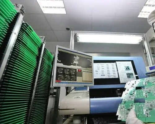
Solder Paste Inspection before Reflow
The last opportunity to correct a print-related defect during SPI occurs before the solder joint has been completed—correcting a paste setting here requires a stencil or program adjustment; a print defect addressed after placement would require a rework cycle, while the same defect found after reflow would require full disposition.
Corrected paste settings should go directly into the next panel’s print program instead of waiting for a review after multiple panels have been printed with the incorrect setting. The reinspected print and its post-reflow follow-up should be combined into one linked inspection record and not treated as two different inspections on two separate passes.
Placement through Post-Reflow Inspection
The inspection process for product placement is separate from the post-reflow inspection of that product. A product that passed pre-reflow inspection and was cleared for reflow will still require its own post-reflow inspection result—the potential impact of reflow on the placement inspection outcome must still be taken into account.
Each inspection stage must use the same version of the placement data, BOM revision, and AOI program; otherwise, a station running last week’s reference against this week’s ECO may pass parts that should not have passed. Any inspection stage that detects a discrepancy should not only flag the discrepancy for the other inspection stage but also indicate that the program for the other inspection stage will need the same update so that both inspection stages do not have to discover the same fix separately.
Hidden-Feature Inspection
Unlike standard feature inspection, which occurs during production, hidden-feature inspection is scheduled during setup instead of being assigned board by board during the actual production process. The package list, expected overlaps, and views are set before production starts, so the operator is not under time pressure to choose an X-ray configuration.
An ambiguous inspection result will be escalated to an engineer to determine the need for a non-standard viewing angle or comparison view; this escalation and its outcome contribute to creating the standard configuration for the subsequent unit of the same package.
First Article Inspection
Any deviations will be identified by feature and location, corrected using the approved procedure, and reinspected. Before reusing the first article of the product, any changes to the PCB revision, BOM, placement data, substitute parts, material set, or process reference will be evaluated.
When a product requires first-article approval, subsequent production will proceed after corrections have been performed and accepted under an approved deviation or otherwise dispositioned in accordance with the governing requirements.
Traceable PCB Inspection Reports
A traceable line links the board revision and lot or serial number to a reference designator or coordinate, inspection method, inspection criterion, image or measurement, initial call, confirmation, action, reinspection result, and final disposition. Any inaccessible features will retain their previously assigned alternate method or earlier inspection point.
Rather than providing only a board-level pass report, the record generated for a BGA or PTH should identify the package or hole region and the image configuration.
Process Feedback from Inspection Findings
Through process and lot correlations, it can be determined whether a single-board event has occurred or whether the event is the result of a repeated condition at the same stencil aperture, feeder, panel position, reflow interval, selective-solder nozzle, handling process, or board-supplier lot.
Repeated signals allow containment to expand across the affected production interval and direct remedial action to the relevant control. Verification will extend beyond the repaired unit to include the following production samples instead of closing the issue on one reworked PCBA.
PCB Inspection Applications

Prototype PCB Inspection
Prototype PCB inspection confirms that the inspected prototype meets the expected configuration based on the latest PCB revision and BOM before the next prototype run or production release. Multiple ECOs, missing references, approved substitutes, or a small sample size create greater reliance on configuration comparison than on lot or trend analysis. The PCB revision, BOM, placement file, polarity reference, and AOI program all need to match. A part that matches the expected outline but is approved for use as a substitute could still have a different polarity mark or package height. Configuration discrepancies between what was intended to be produced and what was produced must be documented separately as a configuration error and not confused with a workmanship error.

High-Volume SMT Inspection
In high-volume production, inspections must detect variations that occur over time and throughout the process without allowing defects to become buried in an overabundance of false calls. Defects are captured through 3D SPI, 2D/3D AOI, targeted visual confirmation, and trend analysis. Each inspection result is collected and analyzed based on aperture, feeder, board position, panel, and production interval. An individual non-critical call may generally require only confirmation; however, repeated defects that occur at the same aperture or feeder must be identified and contained during the process, and the cause must be corrected.
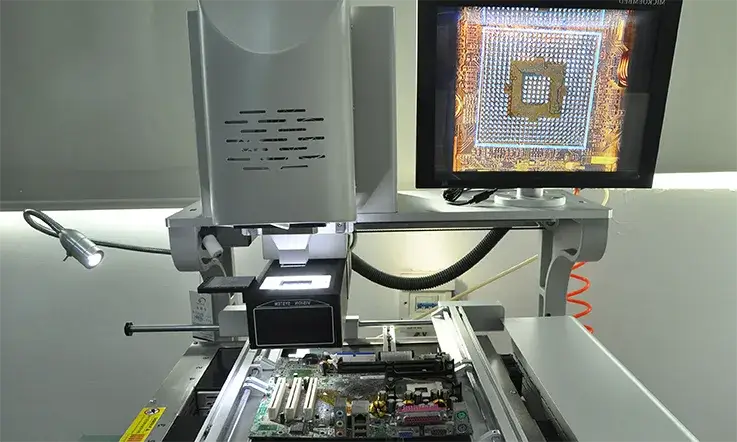
BGA Assembly Inspection
In a BGA assembly inspection, two conditions are examined: (1) the visible condition of the package placement and (2) the hidden condition of the underside solder joints. AOI examines the upper side of the board for the mechanical alignment of the BGA and the mechanical features associated with the BGA and surrounding components, while X-ray evaluates voiding, bridging, insufficient solder, alignment, and suspected interface separation. A finished assembly with double-sided population, copper planes, or via-in-pad structures will have areas of overlap in the top-down image view; therefore, before disposition, the void measurement area and applicable limits need to be defined and cannot be determined arbitrarily during the review stage. An assembly that does not provide sufficient information to determine the joining interface cannot definitively establish whether head-in-pillow or non-wetting is present; the condition remains an indicator until it is positively confirmed.
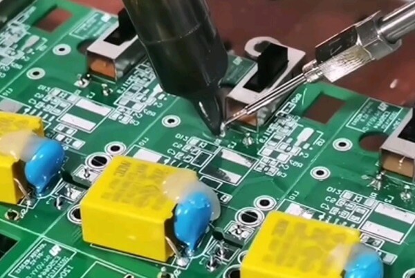
Through-Hole Connector Inspection
Through-hole connector inspections evaluate each aspect of the connector housing—seating condition, pin alignment, protrusion, height or coplanarity, visible fillets, and barrel fill—as separate items. A top-view image will not provide sufficient information to determine all of these conditions. Front, side, and angled views provide inspection of the accessible seating area and pin geometry. A 3D AOI measurement can provide information on height or coplanarity; X-ray allows evaluation of obscured barrel-fill areas that cannot be determined from an optical view of the connector. Press-fit connectors and soldered connectors have different acceptance criteria; the easiest misinterpretation is to believe that if the housing is fully seated, all pins and barrel-fill conditions are also satisfactory.

Medical Electronics Inspection
In the inspection of medical electronic products, the appropriate inspection requirements are determined by the classification of the assembly and the customer requirements for the product. The fact that a product is identified as medical electronics does not automatically mean the assembly is IPC Class 3. Visual inspection, SPI, AOI, targeted X-ray, and FAI are assigned to the critical features and inaccessible joints defined in the inspection plan. The separation of the various inspection results allows traceability of serial or lot identity, revision, initial results, correction, and reinspection history; the final pass will not overwrite these items. A common gap in medical files is a cleaned-up summary with the original failure omitted. Inspection does not replace process validation or functional test acceptance but confirms acceptance against the applicable workmanship criteria.

Automotive Control Module Inspection
Automotive control modules involve fine-pitch SMT, power packages, connectors, and through-hole or selective-soldered features. As no single AOI station will cover the entire assembly, inspection methods such as SPI, AOI, targeted X-ray, visual inspection, and FAI are assigned based on feature access and the approved control requirements. Repeated findings are correlated across stencil, feeder, line, panel position, material lot, and production interval to define containment before they spread across a shift’s output. The automotive environment does not automatically dictate the IPC Product Class for these products. Therefore, the customer drawing, specifications, or documentation governing acceptance will determine the applicable classification.
Our PCBA Production Lines
















Frequently Asked Questions
PCB inspection evaluates incoming board condition, solder paste, placed components, visible workmanship, hidden solder structures, first-article conformity, and post-rework confirmation at the applicable production stages. When considering a supplier’s quote, clarify which evaluation stages are included without an additional charge and which require a separate charge based on how the supplier scopes the work.
Visual inspection, SPI, AOI, X-ray, and FAI correspond to different production stages. It is not enough to know how many methods are available for your PCB; what is more important is understanding which items are not covered by these methods and will need an alternate method or earlier inspection point.
No. PCB inspection evaluates observable or measurable manufacturing features; it does not verify circuit behavior. A PCB can pass visual inspection, SPI, AOI, X-ray, and FAI and still fail electrical or functional testing. Both inspection and testing are necessary and should be reviewed together rather than treated as substitutes.
The PCB inspection setup requires the applicable Gerber or ODB++ data, assembly drawings, BOM, placement data, revision history, Product Class, marked critical features, and customer requirements. FAI and hidden-joint inspection also require the applicable first-article records and package or feature locations.
A PCB inspection report must include the applicable inspection fields and allow all findings to be traced back to where they were found, the method used, and the criteria applied to determine acceptability. When reviewing a supplier’s report, check whether it includes the original call next to the reinspection result, not just the final disposition.
Inaccessible PCB features will be assigned an alternate inspection method or earlier inspection point during setup, before access closes. Request an actual list from the supplier of the features to which this applies on the specific PCB. Common examples include shielded modules or the underside of BGAs.
Reinspection of PCBs is required when an approved corrective action, repair, process change, or product change may affect the original inspection result or inspection condition. The repeat inspection will be performed using the applicable method and criteria at the same PCB feature or defined affected quantity. The report will retain the original inspection result, the corrective action taken, the reinspection result, and the final status of the PCB.