Upload BOM & Gerber
-
Mobile: +86 13312967631
-
Email: sales@sugaintl.com

Prototype PCB Assembly Services
PCB Prototype Manufacturer in China for Prototype Circuit Board Assembly and Engineering Validation
Prototype PCBAs must be created to check that the parts function properly together and fit well before going to low-volume transfer. Each prototype design must be reviewed by SUGA against predefined engineering criteria and the capability of the chosen Shenzhen / Pearl River Delta process resource to assemble the prototype, not the machine list selected to manufacture the PCB.
12 HrsAssembly-Only Turnaround
0.3 mmFine-Pitch Printing
IPC-A-610Workmanship Standard
500+ PcsProduction Ready
What Is Prototype PCB Assembly?
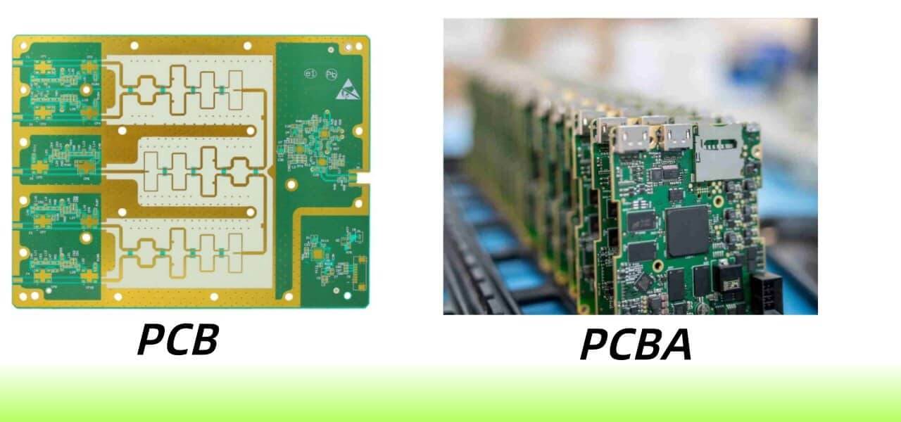
A prototype PCB is a bare board and provides confirmation of fabrication data for creating the product. A prototype PCBA verifies how the assembled circuit functions using real components, solder joints, connectors, firmware, and mechanical fit. The difference between a prototype PCB and a prototype PCBA is that a prototype PCBA is created for engineering validation before low-volume transfer.
The creation of prototype PCBAs can identify PCB layout problems, component compatibility issues, connector interference, firmware response problems, manufacturability issues, and early rework problems.
| Term | Proves | Cannot Prove |
|---|---|---|
| Bare PCB Prototype | Fabrication data, board shape, copper / mask / drill correctness | Powered function, component interaction, firmware response, connector behavior, or assembly workmanship |
| Prototype PCBA | Function, placement, component compatibility, firmware response, manufacturability, early fit and rework risk | Stable production repeatability, stable sourcing, full test coverage, and scaled process control |
| Production Assembly | Repeatable yield, stable sourcing, controlled test process, documentation, packaging, and scale | Early design uncertainty or unresolved prototype findings |

Prototype PCB vs. PCBA
A prototype PCB is still a bare board. It can confirm copper, solder mask, holes, board shape, and layer data, but it cannot verify whether firmware will boot or how a sensor, connector, charger, switch, or interface will function after assembly.
For engineering validation, a prototype PCBA allows engineers to measure the actual functionality of a prototype circuit, check whether the individual components fit, and see how the final assembled circuit functions against the expected circuit behavior.
When A Bare Board Is Not Enough
When the question being asked about a prototype PCB shifts to how the circuit will function when powered, how signals will be transmitted through the circuit, whether firmware will work with the circuit, or how well the components will physically fit into the designed case, assembly validation is necessary for the prototype PCB.
The assembly of prototype PCBs provides an opportunity to validate electrical and mechanical aspects of the prototypes and quickly identify early mistakes made in the manufacturing process.
What A Prototype Cannot Prove Yet
Prototype assembly reduces risk, but it does not solve pilot or production validation issues associated with manufacturing a PCB. One clean sample can still hide repeatability issues, sourcing risk, test coverage gaps, or handling problems that appear only after more boards move through the line.
Many projects pass through 2-3 prototype iterations before production. The right number depends on what the first samples reveal and how much must be frozen before low volume.
Which Service Model Fits Your Prototype?
A complete turnkey service for creating a prototype PCB reduces the purchasing burden on the customer. A kitted service allows the customer total control over specialized parts. A partial turnkey service splits the BOM so that critical items remain under the customer’s control, while the assembly service procures the remaining standard parts.
Before a prototype PCB can be assembled, the customer must determine who will procure the component parts, who will approve substitute components, and how many spares will be made available for setup and rework.
| Assembly Model | Use When | Customer Provides | Handled Work | Confirm Risk |
|---|---|---|---|---|
| Turnkey | Purchasing time is the main constraint and most parts are standard or sourceable | Approved design files, approved BOM, target quantity, test notes, substitution rules | PCB fabrication coordination, standard component sourcing, assembly, inspection, delivery coordination | Approved substitutions, long-lead parts, obsolete parts, test expectations |
| Consigned Assembly | Special, controlled, expensive, allocated, or locked components must stay under customer control | All components, labels, packaging, overage, polarity notes, MSL notes, controlled parts list | PCB fabrication coordination, assembly, inspection, receiving count, issue feedback | Short tape, missing overage, unclear polarity, moisture-sensitive packaging, missing labels |
| Partial Turnkey | Locked ICs or long-lead items sit alongside common passives and standard components | Critical ICs, special connectors, approved alternates, controlled components | Standard passives, sourceable parts, PCB fabrication coordination, assembly, inspection | Split-BOM responsibility, substitution approval path, critical-part release timing |
Turnkey Prototype Assembly
A turnkey prototype assembly is best suited for situations in which there is less complexity in the parts being manufactured than in the time that it will take to purchase those parts. A turnkey arrangement allows SUGA to source standard components, coordinate fabrication, and perform assembly and inspection under one schedule. The buyer still owns the design intent, but the buyer must lock down all information associated with an approved project, including approved design files, BOM, target quantity, test notes, and substitution rules, before SUGA can begin sourcing the required parts.
The bottleneck is less likely to be the parts that are ordered from the approved vendor list than the expected turnaround time on substitutions. If an approved manufacturer part number becomes obsolete or goes end-of-life during the production of a prototype, the delay in production of the prototype will depend on the time required to approve or reject the newly recommended replacement component.
A project that has pre-approved a short list of alternate parts for the highest-risk components avoids downtime during production.
Customer-Supplied Components
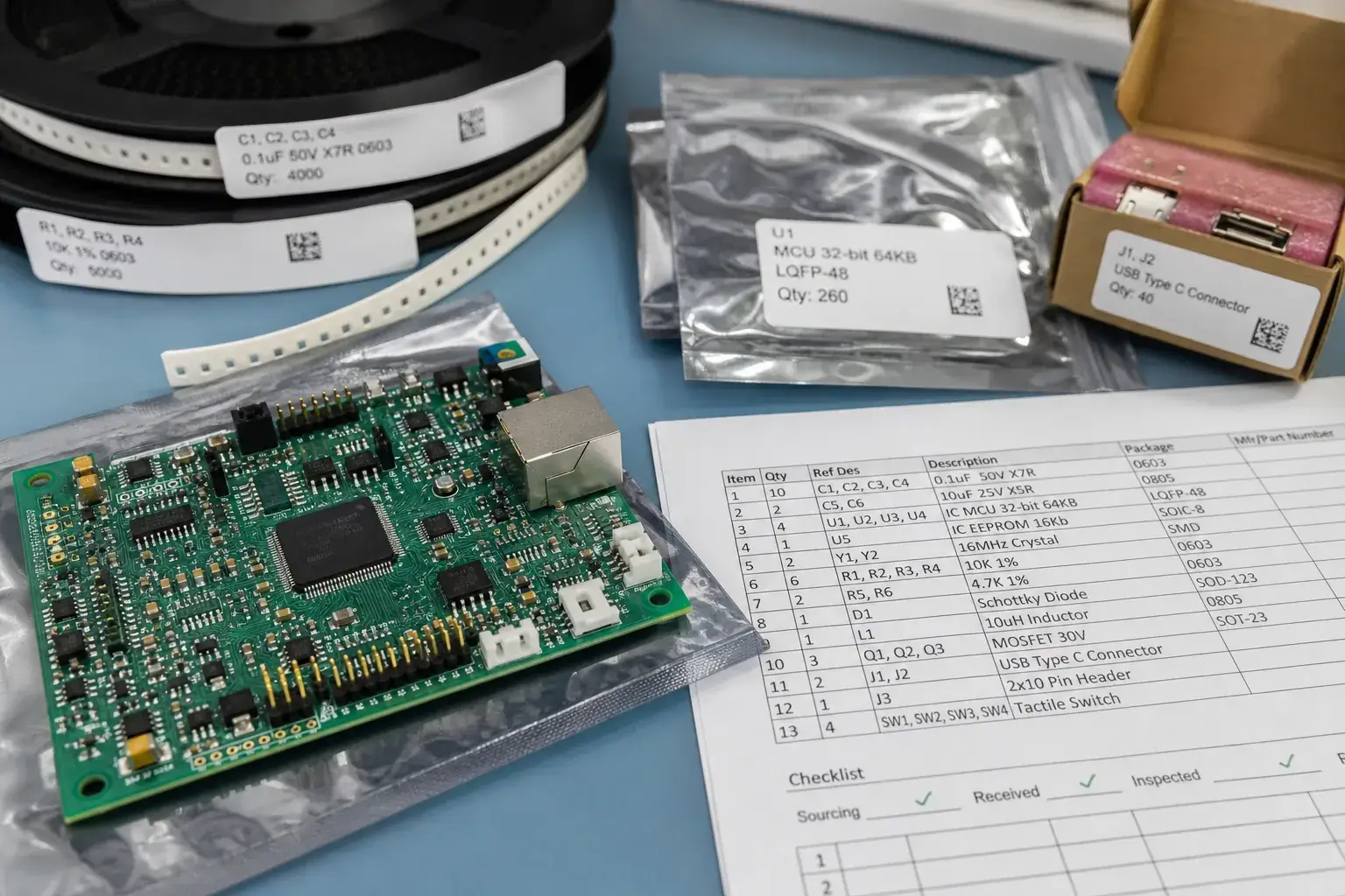
Once the buyer has provided the components for a kitted assembly, the supplier can move the components to the assembly line after checking whether quantity, packaging, labels, polarity notes, and MSL status are workable before placement.
While a kitted assembly provides the buyer with better control over the parts used to produce the assembly, it also increases the risk from the buyer’s preparation work. For example, a short tape count on a supplied component, missing overage on a BOM, or lack of appropriate labels on a component can negatively impact the customer’s ability to produce an approved prototype assembly.
| Component Type | Extra Quantity | Why It Matters | Risk Prevented |
|---|---|---|---|
| 0402 / 0603 / 0805 Passives | +20-30% extra or minimum 20-30 pcs | Feeder loss, handling loss, and rework margin are proportionally higher in prototype quantities | Line stoppage from small passive shortage |
| ICs In Tape / Reel | +2-3 extra pieces | Setup loss and first-article correction can consume parts before final samples are accepted | Delay caused by damaged or consumed ICs during setup |
| QFN / BGA / Fine-Pitch ICs | +1-2 extra pieces, more if short tape | Hidden pads and tight pitch increase placement and rework risk | Inability to rework or repeat a sample when one critical package is lost |
| Connectors / Mechanical Parts | +1 or +2 each | Mechanical damage or fit adjustment can stop the prototype if there is no spare | Prototype stoppage caused by broken connector or fit correction |
| Expensive / Rare Components | At least one spare | A single damaged or lost part can stop the entire prototype lot | Complete schedule stop due to one unavailable component |
Often, teams will stock the most expensive components in greater numbers, such as ICs, and under-stock less expensive components, such as connectors. If a connector is broken or misaligned, the line can be delayed before it ever reaches the point where it needs to use the rare part. The most typical stoppage is not the wrong part, though. It is the right part with the wrong label: a bag containing the proper-value passive components can still be put on receiving hold if the bag does not contain the lot code or date code. The line cannot confirm MSL exposure history after the original packaging has been opened.
Split-BOM Sourcing
When using split-BOM sourcing for a portion of the project, the customer retains ICs, special connectors, or long-lead-time components. SUGA will help source all remaining components, such as standard passive components and other sourceable parts, and coordinate PCB fabrication, assembly, and inspection.
The challenge with the split-BOM model is who will sign off on the “critical” parts. A part that the customer considers “critical” because it costs more than other parts may not be the same type of part that is critical because of a long lead time or because it is single-sourced. The release timeline for a project will depend on what is defined as “critical” for that particular project. If the definition of what constitutes “critical” is established before the BOMs are split, it can eliminate unnecessary back-and-forth once the actual sourcing of the parts has begun.
How Much Extra Material Should Be Prepared?
How many additional spare components should be ordered for prototype quantities? Because setup loss and rework do not scale proportionally to prototype quantities, teams often order more of the expensive IC and less of the connector. Therefore, if a connector is broken or misaligned, the board will not be used, regardless of whether the rare IC is readily available.
Which Assembly Method Fits The Board?
SMT is typically used with densely populated boards. Through-hole is primarily used for mechanical assembly. For prototype connector-plus-IC combinations that require mixed technologies, BGA, QFN, and fine-pitch packages differ in the amount of paste that must be added and how tightly they must be placed together. When planning these types of prototypes, careful attention must be paid to paste volume, placement location, spare part availability, and inspection capability.
SMT For Dense Prototype Boards
For dense prototype assemblies with integrated circuits, passive devices, sensors, compact modules, and double-sided component placement, SMT prototype assembly is typical. The benefits of SMT prototype assembly come from repeatable placement of small components in precise locations. Every SMT job involves some amount of risk, even when multiple jobs result in reliable builds through the assembly line.
The following factors affect whether the first samples will cleanly and correctly pass inspection: feeder setup, stencil quality, placement data, polarity, and passive component handling. To the extent that the package allows it, AOI can assist with solder and placement verification.

Through-Hole For Mechanical Strength
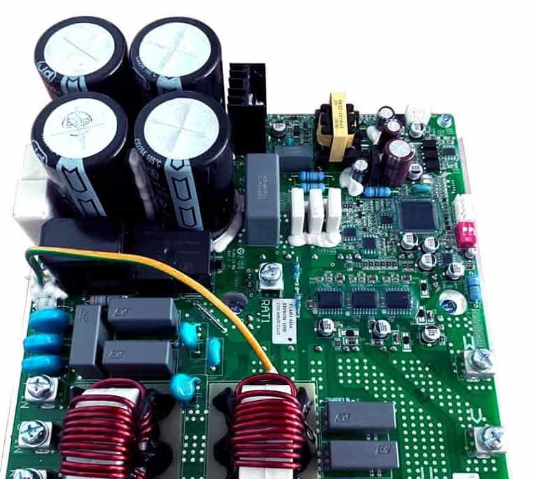
When a product requires mechanical support, connection to field wires, or mechanical retention, THT should be selected. PTH and THT assemblies are typically used for mechanical support structures such as terminal blocks, switches, connectors, power portions, and other high-stress items, but may also be used on the same PCB with dense SMT components.
Common methods are hand soldering and wave soldering, depending on part type and quantity.
Mixed SMT And Through-Hole Boards
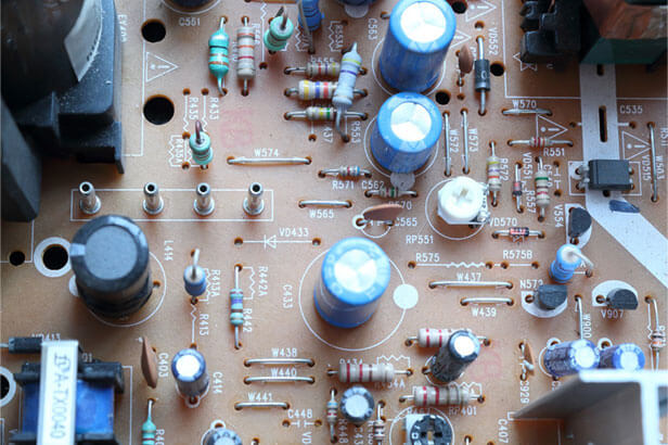
Mixed technology PCBAs combine control ICs with connectors, relays, terminals, or power interface types. Typically, the SMT portion is installed before the THT portion is inserted and soldered. Component position on the PCB and soldering process factors such as connector height, solder heat exposure time, manual handling, and rework access impact the quality of a mixed technology PCB.

Hidden-Joint Packages
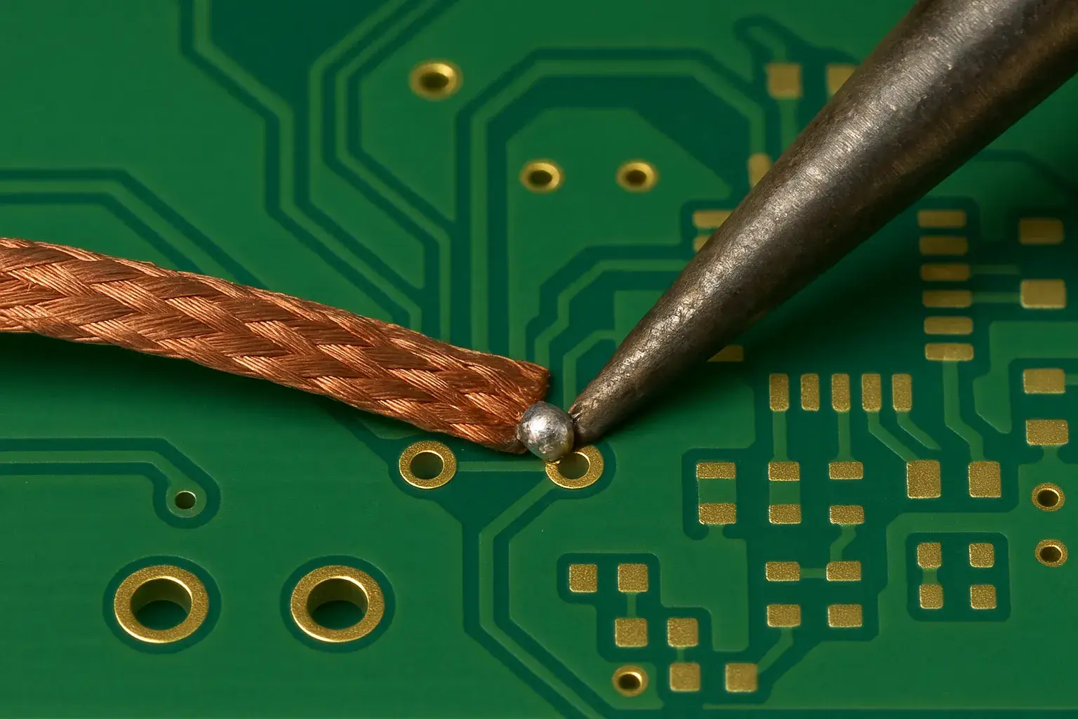
BGA, QFN, and fine-pitch packages conceal risks under the component. The first step to successfully completing the assembly of any BGA, QFN, or fine-pitch package includes checking the paste volume, stencil specifications, placement of parts, availability of spare parts, and inspection capability.
0.3 mm fine-pitch printing is a useful market benchmark for planning. For tight CSP-class projects below 0.3 mm, SUGA can review the package and verify that the tighter process window is appropriate for the project.
Rigid, Flex Or Rigid-Flex?
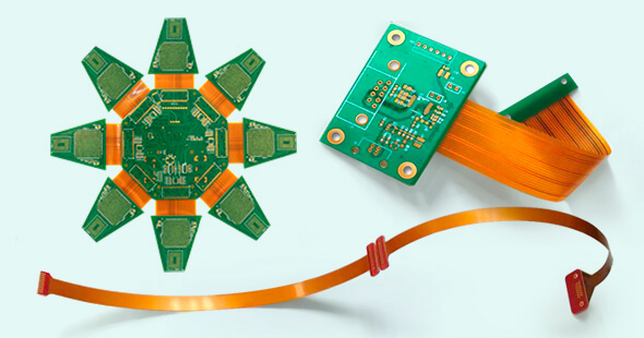
For prototype assembly, consider single-sided, double-sided, multilayer, rigid, flexible, and rigid-flex designs, and how these different designs affect how PCB prototypes are assembled. In terms of placement and reflow planning, double-sided SMT prototypes typically add additional expense and planning time.
Another factor that must be considered when working with flexible and rigid-flex prototypes is whether the assembled PCB can withstand bending in the flexible area, mechanical stress on connectors, and the product enclosure fit required by the customer’s specifications. Validating the assembled product in terms of fit and function should be completed as part of a prototype PCBA since bare-board fabrication does not verify the assembly’s capability.
What Must Be Checked Before Assembly Starts?
Review the following items before starting assembly: fabrication files, BOM, placement information, drawings, notes regarding DNP parts, polarity, component footprints, spacing, and packaging information, to ensure that all inputs represent the same prototype. When discrepancies exist between the listed inputs, they will be carried through the subsequent assembly lines as errors.

| Check Item | Must Match | Why It Matters | If Missing | Risk Prevented |
|---|---|---|---|---|
| Manufacturing File Set | Gerber, drill files, layer notes, board outline, stack-up notes, assembly drawings | Assembly cannot verify copper, solder mask, drill, side, and placement intent without one consistent file set | Delay before assembly starts, or wrong-side / wrong-revision risk | Wrong revision, wrong side, wrong drill, wrong assembly intent |
| BOM / MPN / Substitutions | MPN, quantity, package, approved alternates, DNP marking, lifecycle note | Prototype shortages and wrong substitutions are common causes of stalled PCBA samples | Sourcing delay, wrong part, or unapproved replacement | Unauthorized substitution or stalled sourcing |
| Centroid / Pick-And-Place Data | X/Y coordinates, rotation, board side, reference designators | Placement machines need coordinate and rotation data that match the assembly drawing and BOM | Rotated parts, misplaced parts, or manual correction delay | Misplacement and polarity-related rework |
| Polarity / DNP / Special Handling | Orientation marks, DNP list, manual placement notes, sensitive-part notes | Prototype lots have little margin for rework caused by unclear polarity or population rules | Rework, scrap, or function failure during first power-up | Wrong LED, diode, IC, connector, or polarized capacitor orientation |
| Fiducials / Footprints / Spacing | Fiducials, pad size, footprint match, component spacing, rework access | Automatic placement and solder quality depend on board data matching real component packages | Placement drift, solder bridging, tombstoning, or manual intervention | Placement drift, solder bridging, tombstoning, inaccessible rework |
| Packaging / MSL / Baking | Tape / reel, cut tape length, label, moisture sensitivity, baking note, sealed bag status | Customer-supplied components can fail before placement if packaging or moisture handling is unclear | Receiving hold, baking delay, or damaged components | Moisture damage, line hold, damaged parts, avoidable baking delay |
Assembly File Set
When creating assembly files, all assembly files, e.g., Gerber files, drill files, BOM, centroid data, and assembly drawings, must reference the exact same revision of the board. If one of the files is not referencing the same board revision, the line will inherit the wrong file.
This is how teams get caught off guard when a file set appears to be complete, because all types of files are present, only to discover that the centroid file was exported from a past revision after a last-minute layout change. There will be no indication of the discrepancy in the file naming. The discrepancy will only become apparent when the placement does not match the silkscreen.
Part Number And Substitution Check
The BOM must include the exact MPN, quantity, package, approved alternates, and DNP status. A vague part description is enough for the procurement process to stall before a product is even assembled.
Approved alternates help both parties because they provide SUGA with a pre-approved option for a part that is either allocated or obsolete. They also prevent operators from substituting parts which have not been approved by the buyer. The BOM should include the actual part number of the approved alternate; simply saying an alternate is allowed or equivalent is not sufficient.
Polarity And Population Rules
The DNP markings indicate to the operator which pads are to remain empty. The polarity and orientation notations protect LEDs, diodes, ICs, connectors, and polarized capacitors from first-power-up failures.
Prototype lots are less forgiving with respect to rework than production lots. Prototype lots generally do not have a second board to fall back upon. A polarity note that only exists on the schematic and is not indicated on the assembly drawing is essentially useless to the operator. The operator uses the assembly drawing for guidance, not the schematic.
Footprint And Placement Access
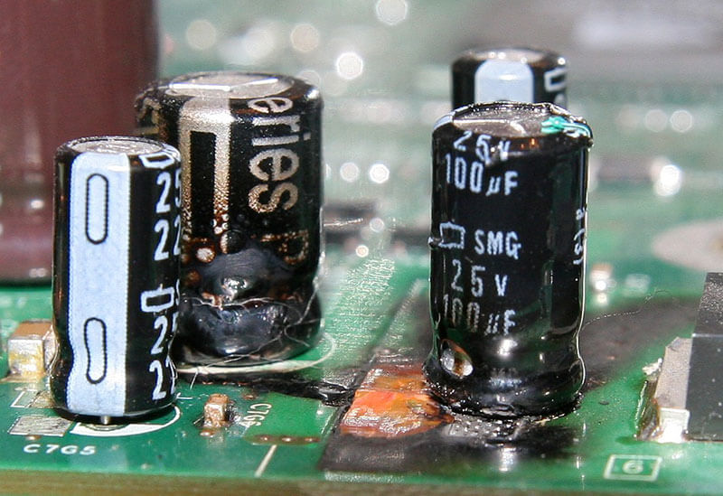
The placement system can be aligned to the board using fiducials. The footprint and pad dimensions will provide confirmation that the actual component package corresponds to what was designed on paper. Spaces between footprints will determine whether a part can be repaired without disrupting an adjacent part, i.e., it can be replaced without removing all surrounding components.
When inspecting a footprint mismatch, this mistake may be perceived as a soldering defect since it creates the same tombstone or bridge appearance whether the error was created by an incorrect aperture on the stencil or a pad that was never sized appropriately for the component that was provided. It is less expensive to identify the footprint mismatch before the placement of components than after AOI.
Component Packaging And Moisture Risk
The moisture risk, meaning MSL, can be established based on the packaging used to store the part and its environment. The packaging must be labelled according to the moisture level, or to the level required by the customer, before it can be accepted for use on the production line.
Baking a component is more of a scheduling issue than a technical one. The typical baking times for LEDs and ICs, 4 hours and 12-24 hours respectively, are component-dependent guidelines, but these baking and subsequent cooling times must be accommodated in the production timeline before any prototype is built. If a baking requirement is discovered after the prototype is started, that baking requirement will likely add a day to the timeline that was not previously planned.
How Does A Prototype PCBA Move Through The Line?
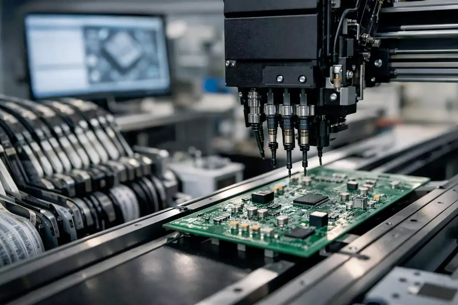
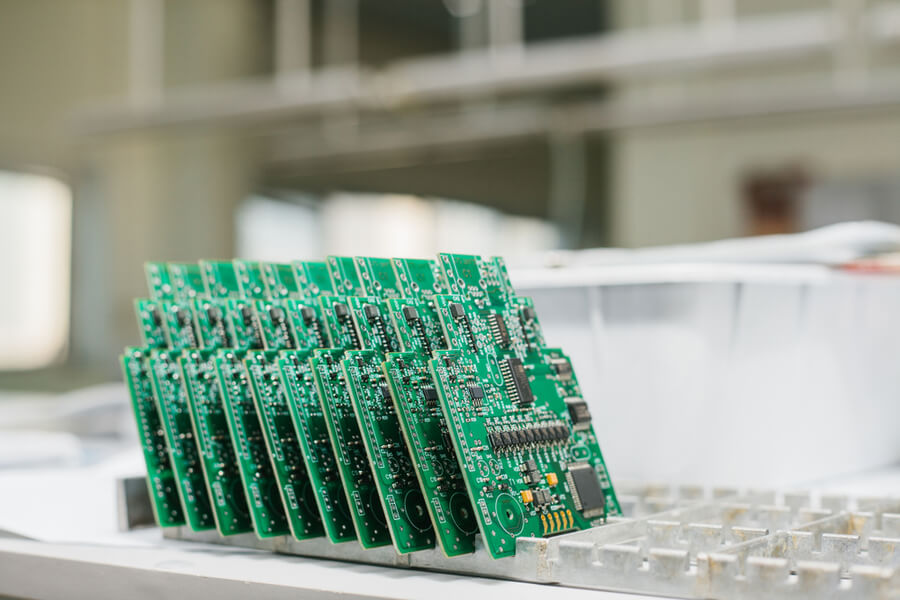
Once all files and parts are received, the prototype PCBA will progress through file intake, parts setup, stencil and paste, placement and soldering, inspection, and feedback to determine if further prototyping is required.
From Files To Work Order
A file set for the SMT, THT, and sample confirmation processes, along with the released parts, is created by converting approved file packages into controlled work orders of the same quantity, BOM, placement data, and test notes that refer to the same prototype lot.
Material Release
Materials are obtained through the selected sourcing model or provided by the customer. Since most standard parts will flow through SUGA sourcing, provided parts will be counted, labelled, and checked for packaging readiness prior to going on the line. By reviewing the incoming materials, the line setup will be protected. Any materials that must be baked or require controlled handling must have those conditions resolved prior to any placement.
Paste And Placement Setup
Using stencil fabrication and solder paste printing to create pads for placing SMT components, and then using feeders, fiducials, placement programs, and polarity data to convert CAD into a line setup, the solder paste and placement setup process manages the quality and accuracy of the data involved with SMT placement. When creating a placement program using stale centroid data, that program may look correct in CAD, but may misalign when brought back to the real board.
Soldering Method
After placement of SMT parts, they generally then go through reflow. THT parts may be hand soldered or go through wave soldering. Boards that contain both SMT and THT parts may require the use of both soldering methods in a controlled order to avoid damaging previous work through heat or handling from later work. Because THT parts soldered after SMT reflow help avoid a second heat cycle on already placed SMT components, they are less likely to loosen or shift from the board’s original position.
First Sample Review
The first sample is critical for feedback. Any visible defects, placement issues, fit issues, and test results specific to the project will be reviewed before further production or pilot quantities are released. Initial samples can also be mounted in an enclosure or wired together for fit or ease of integration testing before more units are produced.
How Should A Prototype PCBA Be Inspected?
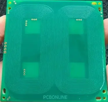
The inspection method must be proportional to the risk. Visual inspections are used to check for visible workmanship or orientation defects. AOI is used to check for visible SMT placement and solder quality. X-Ray Inspection is used to examine hidden joints. Electrical testing is used to measure the continuity of each circuit. Functional Testing must be conducted using controlled conditions.
Each method depends on the package type, net access, functionality, and customer records, depending on what the consequences will be of missing an undetected defect.
| Inspection | Best For | Finds | Customer Input | Risk Prevented |
|---|---|---|---|---|
| Visual Inspection | Readable markings, orientation, workmanship, visible solder joints, mechanical damage | Missing parts, wrong orientation, visible solder defects, damaged components | Assembly drawing, polarity notes, acceptance expectation | Obvious workmanship or orientation issue escaping to power-up |
| AOI | SMT placement and visible solder joints | Placement offset, missing parts, skew, visible solder faults | Reference designators, expected population list, board side data | Visible SMT placement or solder faults missed by manual review |
| X-Ray | BGA, QFN, leadless and bottom-terminated packages | Hidden joint coverage, voiding, bridging, insufficient solder | Package list and inspection priority for hidden joints | Hidden-joint failures that AOI cannot see |
| ICT / Flying Probe | Electrical continuity and manufacturing defects | Opens, shorts, wrong net behavior, simple electrical failures | Netlist, accessible test points, acceptable coverage | Basic electrical manufacturing defects reaching functional test |
| Functional Test | Powered prototype behavior under defined conditions | Firmware boot, measured range, sensor response, interface behavior | Test procedure, firmware, fixture, input conditions, expected measurement range | Vague powered testing with no clear pass/fail result |
| Standards / Records | Acceptance level and documentation expectations | Workmanship class, traceability expectation, compliance context | Required IPC class, project record needs, customer documentation requirements | Unsupported quality claims or missing project records |
Inspection Records
IPC-A-610 and J-STD-001 are the standards for the quality of workmanship and for solder joint quality, with the classes of each standard set by the project specification; these standards are not the default for every prototype.
Factory certifications ISO 9001, ISO 13485, IATF 16949, and AS9100 are certifications of the quality management systems that the factory holds, and the factory will be audited against those certifications. UL is a product or component mark, not a factory certification. RoHS, REACH, and ITAR are considered to be compliance regulations that a project must comply with and are not certifications that a factory holds.
How Many Prototype PCBs Should You Order Before Production?
The quantity of prototype PCBs, as well as the lead time to produce them, depends on factors related to the goals of the learning process during the prototype production, layer count, availability of components, number of SMT placements, number of THT placements, and test burden. A quick turnaround is only available when a complete design package and material flow is established. The number of the quick turnaround is related to the production line, and does not reflect the paperwork related to that line.
When it comes to prototype PCB assembly, price and time to market are typically the first concerns. Effective, low-cost prototype PCB assembly comes from eliminating costly rework caused by avoidable errors, reducing sourcing confusion, limiting unnecessary testing and early scaling to finished products, and not ordering the fewest possible boards.
| Range | Best Use | Risk | Next Step |
|---|---|---|---|
| 1 Pc | Early power-up, firmware bring-up, connector fit, first electrical sanity check | One sample can hide assembly variation and rework risk | Add more units after first fixes are understood |
| 2-10 Pcs | First engineering validation and early user or bench testing | Too few samples for repeatability decisions | Freeze obvious fixes before pilot quantity |
| 11-25 Pcs | Small engineering lot for hardware, firmware, and mechanical validation | Component overage and manual correction can dominate schedule | Prepare controlled BOM and test method for the next lot |
| 26-50 Pcs | Broader validation, distributor demos, or limited field samples | Test burden and sourcing lead time become visible | Decide what must be frozen before low volume |
| 51-100 Pcs | Larger prototype or small pre-pilot quantity when the design is already stable | Placement count, THT count, and test coverage can change timing | Move to low-volume planning after defects are closed |
| 101-500 Pcs | Low-volume production after prototype validation | Not a substitute for production documentation and stable sourcing | Lock BOM, test method, packaging, and inspection level |
| 500+ Pcs | Turnkey production after prototype and pilot lessons are closed | Scaling unresolved prototype issues multiplies rework cost | Use production controls, not prototype assumptions |
Prototype Lead-Time Benchmarks
The following tiers outline the classifications for small/simple lots, standard multilayer production, and long-lead-time or complex projects. The tiers use the same consistent scale throughout the entire production process.
| Tier | Typical Job | Timing | What Changes It |
|---|---|---|---|
| Simple | 1-10 pcs, single design, complete files and available components | 12 hours | Missing files, special sourcing, BGA / QFN inspection, THT work, baking, functional testing |
| Standard | 11-100 pcs, moderate multilayer complexity, materials and placement data ready | 24 hours to 5-12 days depending on layer count and test method | BOM line items, SMT placements, THT count, sourcing, inspection records |
| Complex | 100+ pcs or high layer count, long-lead parts, high-mix builds | 7-20 days | Long-lead parts, documentation, special inspection, fabrication and logistics queue |
How Layer Count Changes Timing
The timing associated with the number of layers in an HDI design is less related to drilling or laminating and more associated with verifying the design after it has been constructed. HDI, impedance-controlled, and higher density placement structures require a higher number of inspection processes, and those inspection processes are not necessarily scalable.
| Layers | Standard | Urgent | Notes |
|---|---|---|---|
| 2-4 Layers | 5-12 days | 48 hours | Small to medium prototype orders when files, components, and inspection needs are ready |
| 6-8 Layers | 7-12 days | 72 hours | Moderate multilayer complexity; sourcing and test method can still dominate the total project time |
| 10+ Layers | 10-15 days | 96 hours | High-layer boards may also need impedance, HDI, high-density placement, and stronger inspection planning |
For example, a 10-layer HDI board’s timing will be calculated based on the highest end of the timing window, and the inspection step will normally take place in the newly created buffer, rather than adding additional time for increasing the number of layers.
What Makes A Prototype Slower?
For complexity and board quantity, the greater the complexity of a PCB design, the longer the time to produce the prototype. The number of BOM line items and their locations in the BOM, for example, will affect the sourcing and setup processes; the number of SMT components placed on each board will affect the time taken to manufacture and the burden of inspection. For example, the assembly and soldering of THT components may require different methods depending on the volume and scheduling of production, manual or wave soldering.
The capability levels described in the tiers below reflect standard capabilities of SUGA for prototype and small-batch production. When a prototyping or small-batch project exceeds the capacity of a tier, custom quotes will be provided.
| Complexity Tier | Board Qty | BOM Lines | SMT Placements | THT Parts |
|---|---|---|---|---|
| Fast Online Tier | 8 PCBs maximum | Up to 15 | Up to 70 | Max 8 |
| Mid-Complexity Tier | Project-dependent board quantity | Up to 20 | Up to 150 | Max 40 |
| Larger Prototype / Small-Batch Tier | 100 PCBs maximum | Up to 40 | Up to 500 | Max 200 |
When To Move Into Low Volume
Low-volume manufacturing will typically take place when repeated samples consistently provide the same result; this will not occur from the inspection of a single, clean finished PCB. When planning for low-volume production of a PCB, the following design items must remain stable: core function, the revision of the BOM, the placement data, the testing method, packaging method, and the inspection requirements.
Prototype PCB production is typically conducted in the range of 1-10 pcs, with low-volume production typically ranging from 10-500 pcs, while any production of 500+ pcs should be done as a turnkey project after the associated pilot project findings are closed.
| Prototype Result | Freeze | Recheck | Next Step |
|---|---|---|---|
| Firmware Boots And Core Functions Pass | BOM revision, placement data, firmware version | Thermal behavior, connector stress, repeatability across more samples | Order a small validation lot before low-volume release |
| Mechanical Fit Is Corrected | Connector position, enclosure clearance, cable routing | Assembly tolerance, handling risk, field-service access | Update drawings and fit-check samples |
| Inspection Finds Solder Or Placement Issues | Corrected footprint, stencil, polarity note, or part package | AOI / X-ray / electrical test coverage | Repeat the affected prototype step before scaling |
| Sourcing Delays Or Substitutions Appear | Approved alternates and critical-part control list | Lead time, packaging, overage, MSL, and split-BOM responsibility | Decide turnkey, kitted, or partial turnkey for the next lot |
Prototype PCB Assembly Applications
What a prototype must demonstrate is the basis for the applications of prototype PCB assembly, whether it is for function, fit, reliability during use, documentation purposes, connectivity, environmental exposure conditions for use, power handling capability, or readiness for transfer. While there are many types of prototypes available from prototype PCB assembly companies, many different types of questions may be posed by potential buyers of prototype PCB assembly services.
Consumer Electronics Prototypes
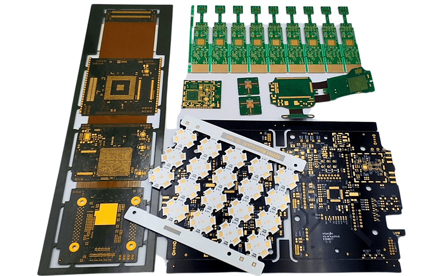
Consumer electronic prototypes exist to address this issue. A wearable device, electronic gadget, or compact Internet of Things board may pass all of the bare-board tests yet fail upon being put into its enclosure because of problems such as connector fit and user interface response. Once the housing for a consumer prototype closes, the placement of the antenna or sensor could also be affected. Packaging tolerance is frequently a hidden variable since a board that fits perfectly into a CAD design enclosure may bind against a real injection-molded part due to the presence of normal draft angle and shrinkage as a result of the manufacturing processes.
Medical Device PCBA Prototypes
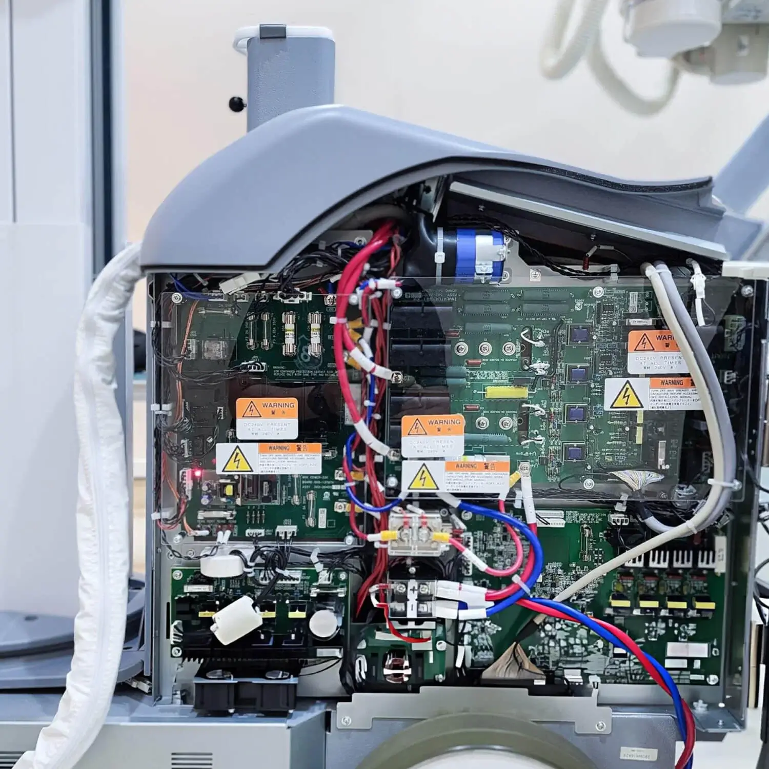
When developing a compact monitoring board using fine-pitch integrated circuits, all of the requirements for the inspection plan must be finalized prior to the manufacturing of the first sample, rather than after. All aspects must be defined: X-ray coverage of hidden joints, documentation of traceability, and criteria for the functional testing under powered conditions. For these reasons, many medical prototype builds can take anywhere from 14-21 days compared to the standard benchmark, primarily due to the documentation burden, as well as the assembly and handling of the medical prototype PCB board.
Industrial Control Prototypes
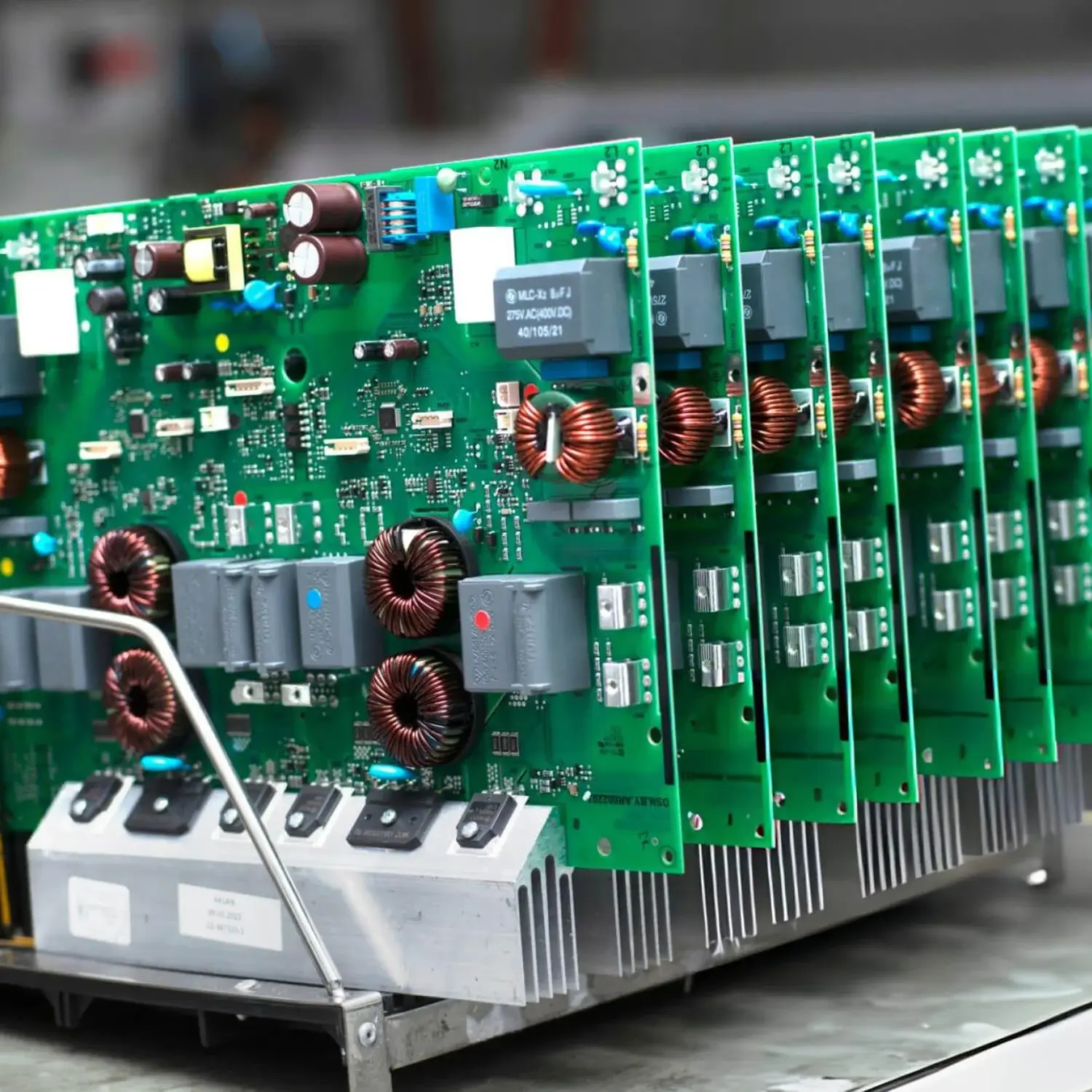
Industrial control boards with integrated circuits require a combination of terminal blocks and relays, which create both a wiring and an assembly problem. Access to wire connections in the field, as well as the cables’ ability to hold the connectors tightly and maintain clearance from other devices, are determining factors for whether the prototype will pass its bench test. Even if a PCB can be inspected under AOI and passed, the end user may find it does not work as intended because when attaching a field connection cable, the technician may torque the connector incorrectly.

Aerospace And Defense Prototypes
The visual inspection process will report on workmanship; however, there will be no confirmation of whether the traceability documents for a project, which will be reviewed during the audit process, were recorded from the first assembly of the prototype if documentation discipline is not required for aerospace and defense prototypes from the start. Therefore, a prototype may look clean at power-up but may not pass the documentation step due to incorrect or incomplete recording of lot codes and processing records prior to assembly.

Automotive Electronics Prototypes
The majority of prototype failures in the automotive industry occur at the interface of electrical performance and the mounting method, and not within the internal circuitry. There are important factors that need to be taken into account for these interfaces, e.g., connector retention under vibration; sensor or control module response and repeatable torque when mounting to an assembly; and firmware or software represents only one aspect of the electronics.

RF And Telecom Prototypes
Controlled impedance boards may have a perfect measurement when tested on a blank test fixture; however, it is common for this measurement to be lost once the controlled impedance board has been assembled. The major contributing factors to this loss of performance may include shielding clearance, high-frequency connector access, test point placement, and so on. The primary concern at the assembly phase of an RF prototype will not be based upon whether the controlled impedance board is assembled correctly or not. It is whether the assembled module can still be probed or measured.

Wearable Fit Prototypes
For example, it is possible that a rigid-flex board passes all bare-board continuity checks but cracks when it is folded into its bend zone for the first time with the connector attached. That is why there is a specific type of wearable prototype and an enclosure-fit prototype to catch that failure early and test the combination of bend-zone clearance, connector alignment, and enclosure space rather than assuming that the flex layer will exhibit the same performance with components mounted as it did in bare-board condition.
Environmental Sensor Prototypes
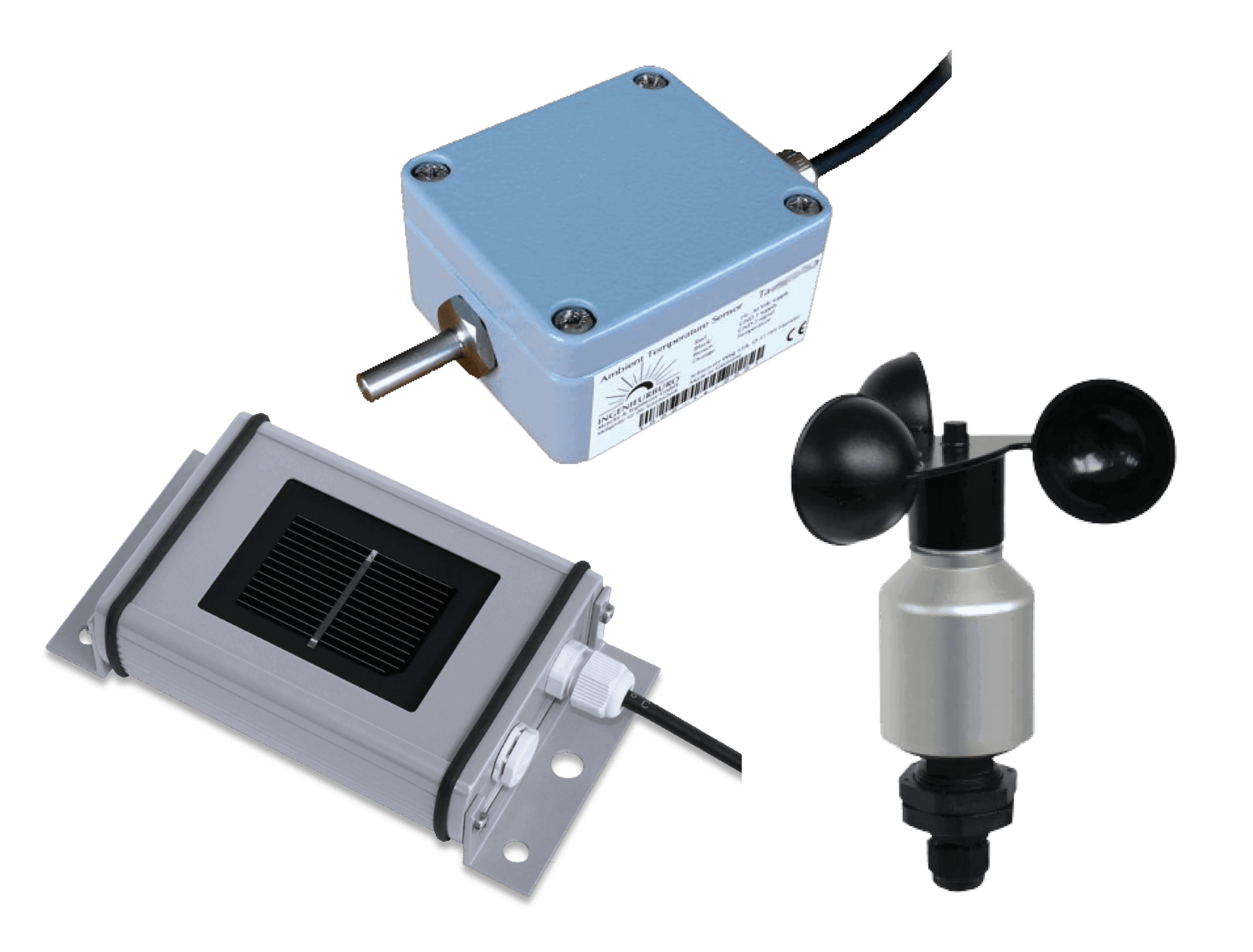
The first question raised by a field-sensor board that cannot be addressed by an indoor prototype is where the sealed boundary is located and whether the coating stops short of the connector or the test point where it needs to be accessible. Therefore, the exposure to moisture, coating keep-out areas, and the functional test requirements need to be confirmed at the assembly level before the design can be committed to a sealing method that will be costly to change.
Power Electronics Prototypes
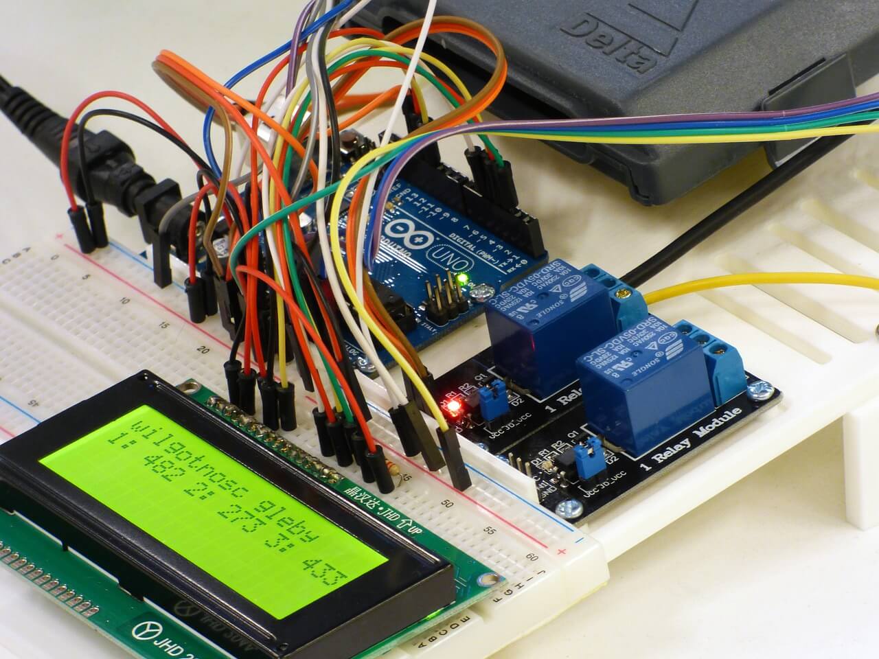
Power prototypes that boot correctly in the bench environment have not been tested for their actual failure mode. Pathways for current carrying, contact with heatsinks or thermal pads, and creepage and clearance to high-voltage nets are only tested when currents are sustained through the boards. This is usually where a design that appears acceptable at room temperature will move outside its clearance margin and start to thermally damage copper.
Robotics And Motor Control Prototypes
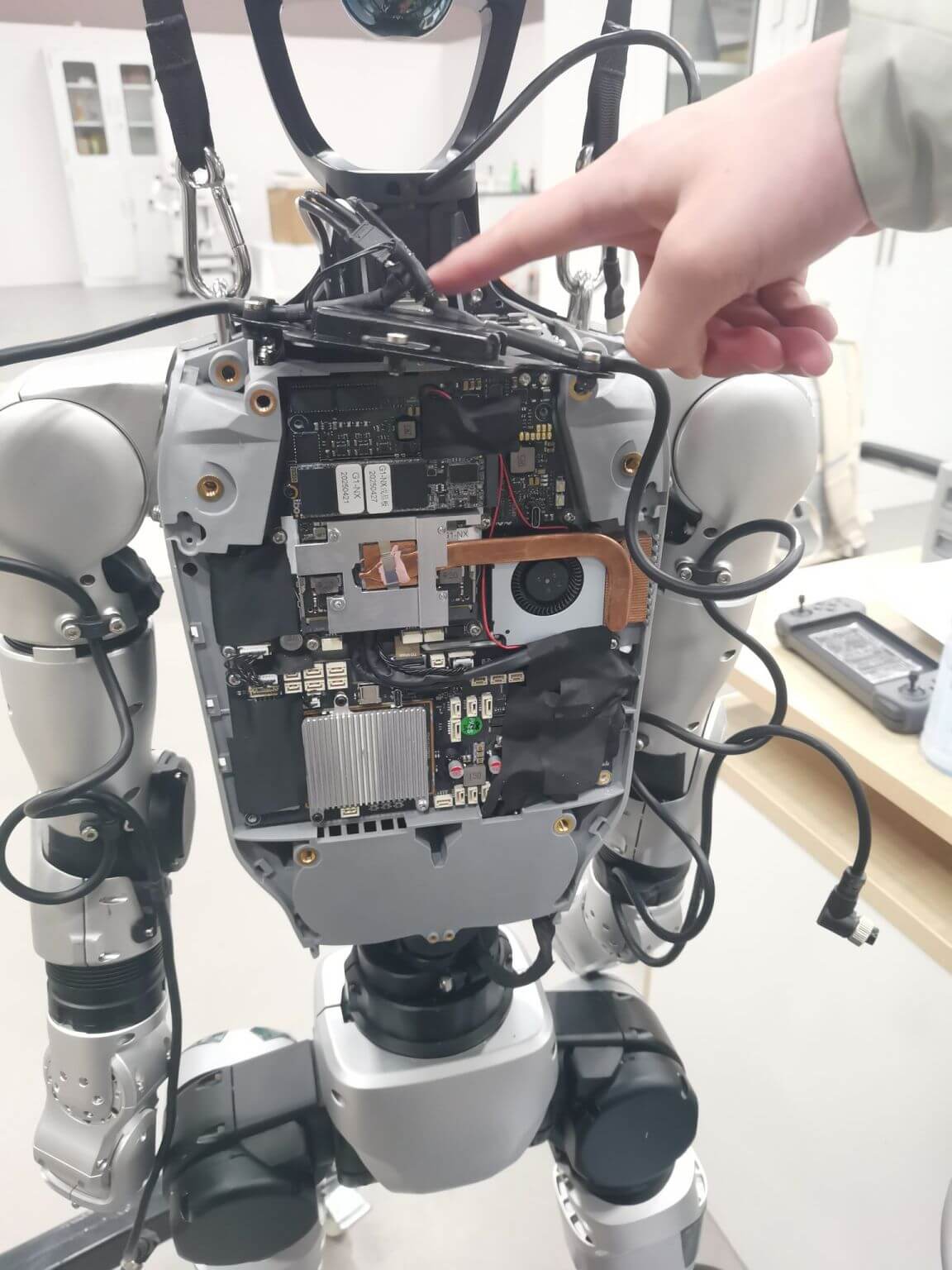
The encoder and feedback interface that fails on a motor controller is typically at the point of motion. Encoders and feedback that are not tested until the controller is in motion are tested when the controller starts to turn and run at speed. Driver-stage placement, thermal clearance, and connector retention under vibration must pass a static continuity check and require functional verification in motion because solder-joint inspection is inadequate to identify when a connector backs out under cyclic flexing.
BMS And EV Charging Prototypes
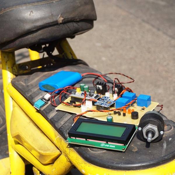
Having a battery management sensing circuit that operates correctly at bench voltage does not mean the same circuit will perform the same way when subjected to actual pack voltage in real operating conditions. All of the factors associated with safety-critical circuitry are more significant than those in traditional prototypes, including isolation, busbar retention, and documentation discipline, because a safety-critical circuit can drift out of specification only once the test factors match the actual operating voltage.
Test Instrument Prototypes
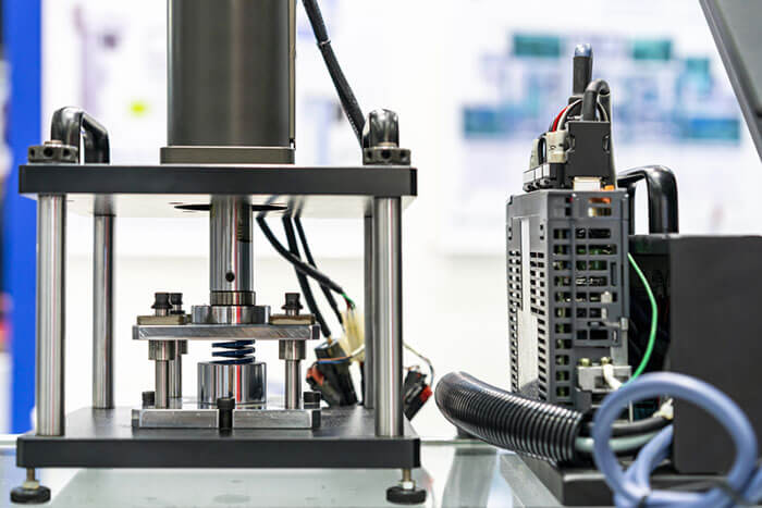
It is possible to have a signal path that measures clean on an open bench and then pick up noise as soon as it passes through a specific test fixture or connector for which it was designed. Low-noise or shielded signal integrity, calibrated interface readiness, and fixture compatibility must all be verified in the actual test configuration and not in the ideal configuration, because the test fixture may also be the source of noise that the bare design never had to consider.
Frequently Asked Questions
The cost of a prototype PCB assembly is directly related to the cost of components, number of boards, stencil requirements, single-sided or double-sided placement, BGA, QFN, fine-pitch packages, THT work, hard-to-find parts, schedule pressures, and coverage of inspection or functional tests.
Prototype assembly can occur quickly if all information regarding files is received in complete format, all components are received and accounted for, accurate placement information is available, and the testing required is limited. Prototypes with lower complexity may meet quick-turn expectations, while other prototype types such as multilayer boards, BGA, QFN, THT insertion, special sourcing, baking, X-ray inspection, or functional testing will extend the assembly schedule.
Yes, prototype assembly can use customer-supplied components if the packaging, labelling, excess overage, polarities, MSL statuses, and substitution rules have been established for those components prior to assembly.
The file set will typically include, but is not limited to: Gerber files; BOM; centroid or pick-and-place data; drill files; assembly drawings; DNP notes; polarity notes; and testing notes if powered checks are to be performed. All file contents must describe the same PCB version. Using file-naming conventions and version numbering that are consistent when packaging file sets, such as an ODB++ or IPC-2581 job package, will help prevent issues that may occur if a Gerber revision and BOM revision drift apart during the prototype build process.
BGAs, QFNs, and fine-pitch components can be assembled if package data, footprint, stencil, solder paste control, placement requirements, required spare components, inspection planning, and sufficient spare parts are ready before assembly.
Yes. The distinction between production and prototype PCB assembly is not related to the assembly process; it is related to the decision. Prototype builds allow us to answer one question: does my design work? Prototype builds are focused on bringing up, troubleshooting, assessing fit, and collecting early testing feedback, all of which take precedence over batch efficiency. Production builds are based on the assumption that the questions related to design have already been answered; therefore, production builds optimize based on repeatable yield, predictable sourcing, and documented processes. The definitive signal that leads one to proceed from prototype assembly to production assembly is not based on the assembly of a “clean board”; it is based on the observation that the same result can be replicated from multiple samples.