Upload BOM & Gerber
-
Mobile: +86 13312967631
-
Email: sales@sugaintl.com

3D Solder Paste Inspection
SPI Inspection Before Component Placement
SUGA uses 3D SPI to measure solder paste deposits after printing and before placement, linking pad-level results to board disposition, reprint decisions, process trends, and downstream inspection records.
5 Paste Measurements
7 Print Defect Signals
Pad-Level Traceability
What Is 3D Solder Paste Inspection?
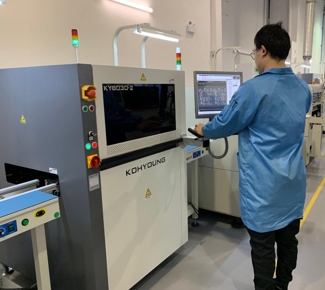
3D SPI is a method used to measure the amount of exposed solder paste after it has been printed through the stencil onto the PCB and before components are placed on top. This inspection uses an optical measurement method, so it does not contact any of the materials involved in the solder paste inspection process. It measures the volume, height, area, and shape of each solder paste deposit, as well as the horizontal and vertical offsets (X/Y) for each pad programmed into the inspection system. It checks the printed deposit, not the component or the finished solder joint.
Where Does 3D SPI Fit in SMT Production?
Within the SMT assembly process, SPI is performed during the transition from the stencil printer to the component placement equipment. Since the PCB still has bare pads, the SPI camera can accurately image the solder paste surface without components blocking the view. Each measurement area of the PCB is linked to the pad geometry defined in the board program, which allows the inspection results to be compared with the limits defined for that particular assembly.
A low-volume deposit, connected paste pattern, or board-wide offset can trigger a hold while the paste is still removable. The operator can then inspect the aperture, stencil underside, alignment, paste roll, separation settings, or board support before cleaning, reprinting, and reinspecting the board.
Why Inspect Solder Paste Before Placement?
3D SPI allows for early detection and correction of solder paste printing problems. A poor print can be identified before it is hidden by components or becomes a problem after reflow soldering. Low volumes of printed solder paste can create open or weak solder joints; connected solder paste can create solder bridges; directional offsets can prevent proper termination coverage. At this stage, it is usually possible to contain the PCB and reprint the solder paste without having to remove components or rework solder joints.
How 3D SPI Works
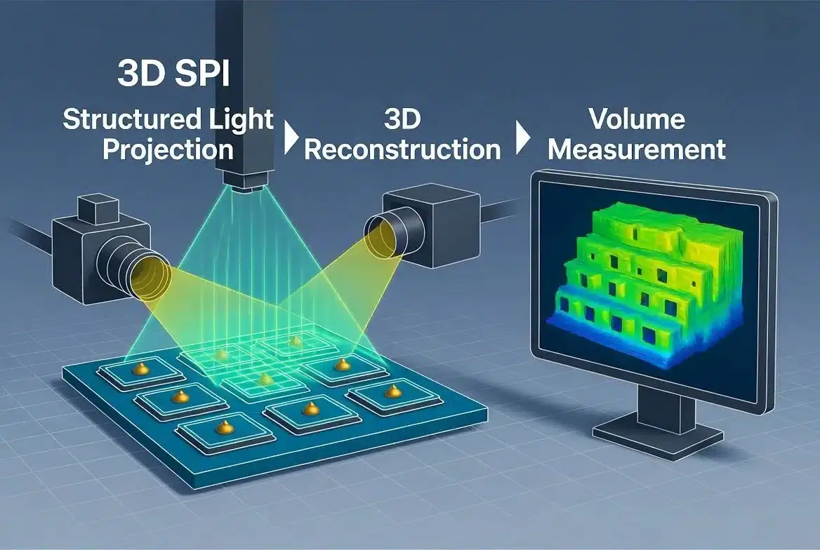
For a system to perform accurately using 3D SPI, it must have the correct board software program, stencil revision, and coordinate alignment. The 3D SPI system captures an image of the printed board and creates a 3D representation of the paste surface, calculates the programmed measurements assigned to that image, compares them against qualified limits, and determines whether the measured deposits match the programmed parameters for the product being manufactured. The final board disposition is recorded against the correct product identity.
How Is a 3D SPI Recipe Aligned?
The program that creates the recipe maps the pad areas of the PCB to theoretical solder paste deposits. The program contains its revision and the stencil revision, as well as the inspection areas and limit set for the board.
When a board is received by the 3D SPI system, its barcode or 2D code provides product identification and calls the correct inspection program. The fiducials establish the X/Y position and rotation of the board, and the reference calibration target checks the measurement reference. The FAI check confirms that the inspection areas identified by the program match the printed board and the same board revision as the recipe.
Optical Image Capture
The configured system projects structured light (phase-shift patterns) or laser-triangulation patterns (projection grid) onto the surface of the PCB and solder paste. The camera system records how the projected pattern changes across the solder paste surface, pad edges, and the local board plane.
A camera taking images of a printed solder paste deposit from only one viewing angle may lose the edges of the deposit as a result of shadowing or reflected light. Therefore, when multi-angle cameras or multi-projection optics are supported and required, the system can capture more of the printed solder paste deposits from multiple viewing angles.
PCBs inspected using 3D SPI must be supported properly during the inspection process. A PCB that is warped, flexed, or rigid-flex can shift the local height datum even when solder paste has been applied correctly. Therefore, surface compensation, rail setup, carrier support, and repeatable conveyor handling must separate substrate movement from an actual paste-height change.
Calculating 3D Solder Paste Measurements
The software uses the data from the projected structured-light capture to create a height map or point cloud. It uses the information contained in the height map or point cloud to establish the board-surface datum from which it calculates the volume of paste on the PCB and the separate calculated heights of each programmed deposit. In addition, the reconstructed surface provides the average height, footprint area, edge shape, symmetry, and centroid offset of the programmed solder paste deposits.
Each of these outputs is related but cannot be used interchangeably. For instance, two printed solder paste deposits can cover the same physical area, but one deposit can have significantly more volume because its height is greater. Therefore, the calculated centroid of each deposit is often used to determine whether there is an out-of-spec alignment error, even when the printed area appears acceptable. The measured volume of each deposit differs from the theoretical volume. The theoretical volume is determined by multiplying the stencil aperture area by the stencil thickness and then accounting for the established paste-transfer baseline.
What Happens After a Failed SPI Result?
After a failed 3D SPI inspection result, the affected board must have a disposition record before placement on the assembly line. Depending upon the defect type, paste condition, board finish, and approved process, the line may hold the board, confirm the call, remove the paste, clean, reprint, reinspect, or scrap the board.
While the alarm on the 3D SPI inspection machine indicates which measured condition has occurred, it does not indicate the root cause of the problem. A thorough root-cause analysis must be performed to identify potential relationships between the affected stencil aperture or area of the PCB and recent prints, including cleaning intervals and similar structures used for printing. Further analysis is necessary to review the paste type, storage and age, changes in handling methods between prints, changes in printing or inspection settings, and the separation settings or alignments applied to the boards during the inspection process. Before an SPI limit or printer setting is changed, the review must also confirm stencil condition and board support.
3D SPI Measurements and Inspection Limits
3D SPI measures the geometry and position of every exposed solder paste deposit and compares the results with validated inspection limits. Therefore, valid SPI inspection measurement limits must come from stencil-aperture theory, pad geometry, stable production data, measurement capability related to environmental factors, and customer specification requirements.
| Metric | Calculated output | Reference basis | Process indication | Disposition logic |
|---|---|---|---|---|
| Volume | Integrated deposit volume | Aperture area × stencil thickness; transfer efficiency; qualified pad-family baseline | Low/high transfer; release variation; regional or time-based drift | Apply pad/package-family limits; investigate recurring distribution shift |
| Height | Maximum, mean, or profile height | Stencil thickness; compensated board datum; stable print baseline | Thickness inconsistency; datum shift; squeegee or release variation | Separate paste change from board-datum or support movement |
| Area | Deposit footprint | Aperture geometry; pad area | Incomplete coverage; spread; smearing; poor release | Correlate with height and volume; do not disposition by area alone |
| X/Y offset | Centroid deviation from pad center | Pad width/gap; package geometry; directional placement risk | Registration error; stencil stretch; fiducial shift | Apply directional pad limits; classify local vs. board-wide shift |
| Shape | Edge profile, symmetry, and form | Aperture geometry; qualified deposit signature | Smearing; tailing; aperture-edge damage; unstable release | Inspect stencil condition and print-separation behavior |
Paste Volume Against Stencil-Aperture Theory
During the development of an aperture family, the gap between the theoretical aperture volume and the actual paste volume deposited on the pad is an important diagnostic measurement. It also indicates expected process loss when it remains stable. When the difference between these two values grows, the gap indicates that a potential release problem is developing and that action should be taken before the problem appears as a limit violation. Paste transfer efficiency—the volume deposited on the pad divided by the theoretical aperture volume—provides a useful way to compare the deposited paste with the intended deposit without treating all aperture families as identical.
The factors that affect release include aperture area ratio, stencil thickness, paste rheology, surface finish, aperture treatment, and package geometry. Therefore, SUGA establishes separate baselines for relevant pad or aperture families and uses FAI verification and stable production data to confirm that the patterns and tolerances remain valid. Production limits are tightened or widened only when stable data and measurement capability support the change.
Paste Geometry Beyond Volume
The area, height, volume, offset, and shape of a paste deposit address different questions. For example, two paired pads may have acceptable individual volumes but still show an imbalance associated with tombstoning risk. The same directional offset can have different implications depending on the accompanying measurements: with unchanged height, it may indicate registration error or stencil stretch, while a local height shift is more likely to indicate board movement. Therefore, the disposition rule should use a combination of measurements rather than any single measurement in isolation.
Setting 3D SPI Inspection Limits
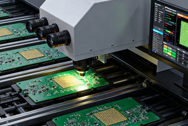
Limit setting for 3D SPI inspection starts with the intended deposit and then uses FAI results, measurement capability, stable process distributions, customer specifications, and package-specific risk factors to define acceptable production limits. The program must retain the stencil revision and paste condition, along with the pad or aperture family used to determine directional offsets. It must also retain any paired-pad logic used to reach a decision.
J-STD-005B provides guidance for the qualification, characterization, testing, and classification of solder paste. IPC-7525C provides guidance for stencil design, IPC-7527 provides guidance for solder paste printing, J-STD-001J provides requirements for the soldering process, and IPC-A-610J provides acceptance criteria for assembled products. However, none of these documents provides one universal SPI volume percentage for every pad and package.
Customer drawings and process specifications are converted into board-level limits only after the measurement system is capable of distinguishing the required change. Limits that reject a stable distribution create false calls, while limits that accept a genuine shift allow escapes. The defined window should therefore be supported by repeatability data and a homogeneous population of pads or apertures rather than one percentage applied to the entire board.
Solder Paste Defects Detected by 3D SPI
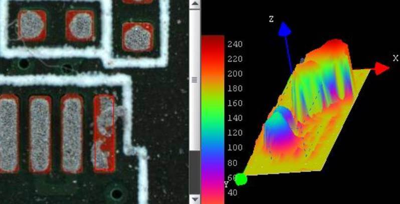
An out-of-limit deposit measurement generates an alarm. The location of the defect and any associated drift must be evaluated against stencil, paste, support, and printer conditions before the cause of the defect can be established.
| Defect signal | SPI indication | Likely print cause | Containment action | Drift pattern |
|---|---|---|---|---|
| Insufficient paste | Low volume or height | Blocked aperture; poor release; pressure/speed or paste change | Hold; inspect aperture/settings; clean, reprint, and reinspect | Same-aperture recurrence; rising low-volume rate; regional decline |
| Excess paste | High volume or height | Paste roll; separation; pressure/speed combination | Hold; check paste roll, settings, stencil underside, and next print | Regional or board-wide upward shift |
| Paste bridging / connected deposits | Connected deposits or printed gap below limit | Aperture design; slump; contamination; alignment; separation | Stop placement; correct print condition; reprint and confirm separation | Recurrence by pad gap or print direction |
| Offset / misalignment | Centroid outside directional limit | Registration; stencil stretch; local support; fiducial error | Confirm fiducials/alignment; classify local vs. board-wide; check next print | Directional shift by region or full board |
| Missing paste | No deposit or below detection floor | Blocked aperture; dried paste; poor release; PCB contamination | Hold; clear aperture/contamination; reprint and reinspect | Same-aperture recurrence |
| Shape defect | Distorted edge, asymmetry, or tailing | Aperture-edge damage; unstable release; separation or paste change | Inspect stencil edge, underside cleanliness, and separation | Progressive or direction-dependent deformation |
| Smearing | Paste outside intended footprint | Stencil-bottom contamination; support; separation; excess spread | Clean stencil underside; confirm support; inspect next print | Concentration by travel direction or cleaning interval |
Tracing Solder Paste Printing Defects
An isolated aperture alarm cannot be treated as a regional or time-based shift. Before changing an SPI limit, confirm whether the pattern follows one aperture, one board region, the print direction, the cleaning interval, or the full board. A limit adjustment is not corrective action when the stencil, support, paste handling, or printer condition has changed unless its relationship to the observed defect has been confirmed.
How Does SPI Fit Into Assembly Inspection?
SPI is a tool used to verify the printed paste deposit before component placement. Subsequent inspection stages, including AOI and X-ray, assess the physical placement of components, the quality of visible solder joints after reflow, and the internal structure of solder joints.
Defect Visibility by Inspection Stage
Once a component is placed on top of a pad, an optical inspection system cannot recover the condition of the original printed paste surface or its geometry before component placement.
SPI cannot verify component polarity, the quality of the solder fillet after reflow, or the internal structure of the solder joint between a BGA or QFN device and the PCB assembly. Pre-reflow AOI checks component presence, intended location, and orientation. Post-reflow AOI checks the condition of components and visible solder joints. X-ray inspection is used in addition to AOI when the required evidence is inside or beneath a package.
What Inspection Follows SPI?
After SPI, pre-reflow AOI can check component presence, intended location, and polarity after placement. Post-reflow AOI checks the condition of components and the quality of visible solder joints. BGA, QFN, and other internal solder joints are checked using X-ray inspection in addition to AOI when required.
Although manual assessment is not a replacement for repeatable pad-level volumetric measurement of solder paste at production rates, it is useful for FAI, unusual contamination, ambiguous machine calls, and rework assessment.
Closed-Loop SPI Process Control
The closed-loop SPI process control system links pad-level measurements to printer and cleaning actions, response rules, SPC data, board traceability, and downstream defect correlation. Process recovery must be confirmed on subsequent prints before returning to normal production operations.
Print-Process Response Rules
Print-process response rules are applied when repeated offset or volume drift occurs. This drift can trigger printer alignment, squeegee adjustment, paste-condition assessment, or cleaning of the stencil underside. Local shifts and board-wide shifts follow different response rules. The response may run automatically through a supported connection or follow an engineer-defined instruction. The next printed board must confirm recovery before normal production operations resume.
Detecting SPI Process Drift
One pass/fail result represents only one board. Distributions, alarm frequency, X-bar and range charts, and regional trends indicate whether the process is drifting. Capability values should only be calculated from a stable recipe and a homogeneous pad or aperture family with meaningful upper and lower limits. Combining dissimilar deposits into one Cpk value can mask drift and produce false alarms.
SPI Data Traceability
An SPI traceable record permanently connects the PCB or panel to the product revision, recipe and limit revision, stencil revision, calibration state, pad-level results, alarm location, operator or review-station decision, reason code, and final disposition. The traceable SPI record supports lot containment and correlation with placement, reflow, AOI, X-ray, and electrical test data.
Cross-Process Correlation
Cross-process correlation allows engineers to evaluate results by matching the board ID, pad or component location, and timestamp across SPI, placement, reflow, AOI, and X-ray. When a downstream defect occurs where a measurable SPI volume or offset shift was recorded, engineers can determine whether the print limits predicted the outcome. If SPI remained stable, placement or reflow becomes the stronger investigation path.
Correlation also supports false-reject analysis and controlled limit changes. The audit trail must retain the previous limit, supporting data, approver, program revision, effective lot or time, and decision rule so that future records can be evaluated against the correct program state.
| Control function | Data / interface to verify | Engineering use |
|---|---|---|
| Recipe generation | Supported CAD/data input, teach mode, or qualified reference-board programming | Define pad regions, theoretical deposits, coordinates, and initial limits |
| Board identification | Barcode, 2D code, serial number, product and program revision | Bind the PCB to the recipe, stencil revision, and inspection record |
| Statistical control | Pad-level results, distributions, control charts, regional trends, alarm rate | Detect drift before repeated out-of-limit printing |
| Board-transfer handshake | SMEMA or equivalent line-transfer handshake | Coordinate conveyor transfer; this alone does not transfer full board identity |
| PCB identity transfer | IPC-HERMES-9852 when licensed and configured | Transfer board identity and product data between configured line machines |
| Factory data exchange | IPC-CFX, SECS/GEM, or selected factory-data interface when supported | Exchange enabled machine state, alarms, results, and production fields |
| Software integration | Configured machine, printer-feedback, MES, database, or dashboard connector | Connect only the messages and fields validated for the production workflow |
| Reporting | PDF, CSV, XML, image, height-map, or database record supported by the system | Support traceability, containment, trend analysis, and quality records |
Configuring 3D SPI for Production
The setup for 3D SPI production starts with selecting the SPI configuration based on production specifications such as minimum pad and gap sizes, board envelope, warpage, cycle time, measurement capability, data interface, and line conditions. The qualified production program uses a single configuration instead of blending limits from multiple configurations across different systems.
2D or 3D SPI?
When the disposition of the PCB relies on measured height, integrated volume, three-dimensional shape, paired-pad balance, or local-surface compensation, the SPI solution needs to be 3D. On the other hand, if evidence of area, presence, and position is sufficient, 2D SPI may suffice. The decision to use 3D or 2D SPI should be based on an assessment of defect risk, pad geometry, board movement, and the production control plan. The package name alone should not determine the selection.
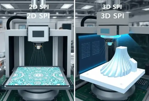
| Selection factor | 2D evidence | 3D evidence | 3D selection trigger |
|---|---|---|---|
| Deposit area | Two-dimensional footprint | Footprint with deposit height and form | Area must be evaluated with height and integrated volume |
| Position / offset | Two-dimensional position | Centroid position with height and shape context | Offset must be separated from shape distortion or local datum movement |
| Height | Not directly measured | Direct height/profile measurement | Stencil thickness, paste height, or local datum changes disposition |
| Volume | Inferred or unavailable | Integrated reconstructed volume | Equal-area deposits may carry different paste amounts |
| Paste bridge / separation | Visible connection or reduced gap | Connection with 3D profile and shape | Fine gaps, slump, or vertical profile increase bridge risk |
| Shape | Visible outline | Edge, symmetry, tailing, and 3D profile | Release quality or aperture damage must be distinguished |
| Surface compensation | Setup-dependent | Height compensation on supported systems | Thin, flex, rigid-flex, large, or warped boards move the datum |
| Fine features | Area/position control | Volumetric control of miniature deposits | 01005 imperial / 0402 metric, 0201 metric, QFN, BGA, narrow QFP, or small gaps |
| Process control | Presence, area, and position checks | Quantitative limits, pad trends, and volume feedback | SPC, traceability, drift detection, or printer feedback is required |
How Is SPI Measurement Capability Proven?
Each SPI measurement capability is established as follows: resolution is defined as the smallest increment that can be reported or distinguished. Resolution should not be confused with accuracy. Accuracy is determined by comparison against a controlled, traceable reference, whereas repeatability is established by measuring the same target multiple times using the same equipment under controlled conditions. GR&R evaluates measurement variation against the manufacturer’s decision limits, including the defined sources of reproducibility.
Calibration targets are used to verify the accuracy of measurement systems. Repeated testing of the same target verifies SPI equipment repeatability, while GR&R evaluation demonstrates whether the SPI measurements are adequate for production purposes. When performing a production study, representative boards and pad families should be used. The study should record the optics, recipe, paste condition, and environment, including temperature, humidity, and elapsed time. It should also include pad geometry, tolerance, sample plan, and whether the GR&R value is reported as a percentage of study variation or tolerance. A GR&R value below 10% has little meaning unless the denominator and actual decision limits are provided.
Balancing SPI Resolution With Cycle Time
High-resolution imaging improves the measurement of deposit edges and small deposits but increases the number of fields, projections, and calculations required to inspect a single board. Resolution, field of view, projection count, and cycle time need to be qualified as one production configuration instead of being selected from unrelated maximum specifications.
Configurations should be compared in seconds per production board, including board loading, fiducial search, selected resolution, projection count, pad count, board transfer, review calls, and final disposition rules. The actual cycle time for a production board determines whether the SPI system supports the line’s takt time.
Handling Warped PCBs
The selected SPI configuration should allow safe transport of the actual PCB without transport or support movement being interpreted as a false height signal. Several variables, including board envelope, thickness, weight, rail margin, underside clearance, carrier design, local flexibility, and the verified compensation range of the system, should be examined together on the production board.
The production trial should include rail engagement, top and bottom clearance, transport height, support tooling, local flex zones, and repeated passes through the conveyor. Thin boards and unsupported transition zones can generate more datum movement than a large, rigid assembly.
Factory Software Compatibility
Verify the actual software license, machine version, report schema, board identity field, MES mapping, and printer-feedback message required by the selected line. The mention of an interface name does not confirm that the required alarm, pad result, recipe revision, or disposition field is available. The message and recovery process must be tested with the production configuration.
Controlling False SPI Calls
False-call performance is influenced by optical parameters, surface compensation, measurement stability, region programming, pad-family limits, and review rules. Controls for false rejects and false accepts should be established using calibration, repeatability studies, representative boards, FAI distributions, multi-angle imaging where applicable, threshold analysis, and confirmation of recurring exceptions before limits are changed.
The review record should include the original machine call, the associated image or height-map evidence, the reviewer’s decision, the reason code, the program revision number, and the final board disposition.
How Early SPI Detection Reduces Manufacturing Cost
A failed board at the print stage can often be cleaned, printed again, and reinspected. A failed board after placement or reflow may require component removal, pad cleaning, joint rework, electrical diagnosis, containment, or a line interruption. The greatest savings occur when paste-related defects would otherwise be identified after valuable components or completed assemblies have entered the manufacturing process.
3D SPI Applications

Fine-Pitch HDI Assembly
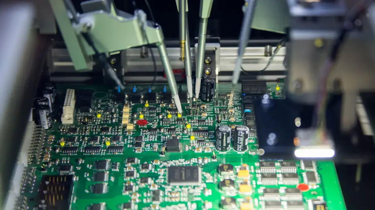
Fine-pitch HDI assembly and fine-pitch assembly typically use small apertures with narrow spacing and deposit patterns that are specific to the package. Therefore, using area alone to determine good release may mask poor release. The critical checks are transfer efficiency, paste separation, and paired-pad balance. One weak aperture can result in an open condition, and unequal deposits applied to miniature passive components increase the risk of tombstoning. The SUGA system tracks these conditions for all assemblies before the placement of 01005 imperial / 0402 metric, 0201 metric, QFN, BGA, and fine-pitch QFP components.
High-Mix and NPI Production
High-mix production and NPI production differ from repetitive production because changes to product revisions, stencils, pad areas, and FAI conditions occur more frequently. A key risk in these processes is that a valid recipe may be applied to the incorrect board or stencil revision. SUGA connects the barcoded PCB to the qualified program, verifies the fiducials and inspection areas during FAI, and establishes a new distribution rather than carrying over an old limit created for the previous design.

Automotive Electronics
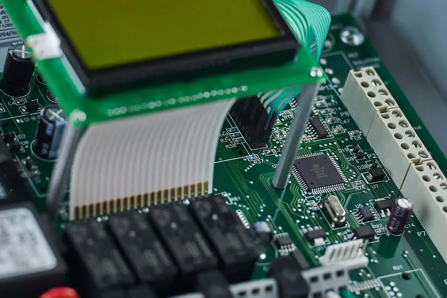
Control and interface boards in the automotive industry are commonly manufactured in repeated lots. Stencils become worn, and the required stencil underside-cleaning intervals vary with the number of PCBs produced. Therefore, production may continue under the same pass/fail view until gradual registration drift has affected several PCBs. SUGA tracks aperture-family distributions, regional X/Y movement, recurring alarms, and lot identities so that any corrective action required to contain a slow shift can be linked to the affected boards before placement.
Medical and Aerospace Electronics
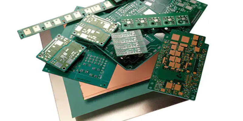
Medical assemblies typically require traceable evidence for sensor, calibration, alarm, or critical high-risk interconnect regions, while aerospace assemblies usually require strict configuration control and lengthy record-retention periods. SUGA maintains the recipe revision, stencil revision, calibration state, pad-level result, exception decision, and final disposition for each board or panel to ensure that approved limits or corrective actions can be traced to the specific controlled lot.
Telecom and 5G Infrastructure
Large telecom and 5G boards may integrate BGA and QFN areas, shield-frame deposits, fine-pitch connectors, large copper areas, and local height variations. The main risk is that a local datum shift may be identified as a paste-height defect, particularly in regions with large copper areas or shield footprints. SUGA qualifies board support and surface compensation and applies region-specific volume, offset, and shape rules instead of a single limit across the entire PCB.
Consumer and Wearable Electronics
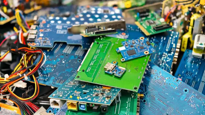
Compact consumer and wearable PCBs may use miniature passives, battery connections, antennas, and displays with tightly packed pads in a narrow print area. It is often critical to evaluate the imbalance between paired pads because even small differences can contribute to tombstoning. Paste spread near RF keep-outs or connectors may also create local bridging risks. SUGA applies package- and region-specific balance, separation, and offset rules before high-speed placement.
Industrial Control Systems
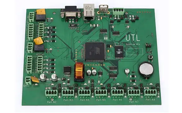
Industrial control PCBs typically include fine control circuits, communication interfaces, terminals, and power components. A single percentage window may be too tight for large thermal or power apertures while being too loose for fine-pitch control devices. SUGA categorizes boards into homogeneous pad and aperture families and applies local limits to each family. Paste release, smearing, and drift are also monitored throughout long production runs.
Flex and Rigid-Flex Assemblies
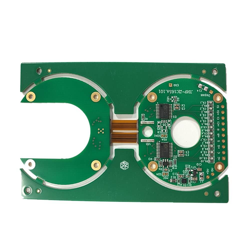
Flex and rigid-flex assemblies must have a stable datum across the flex areas, rigid sections, transition zones, and carrier interfaces. The principal risk, particularly at flex-to-rigid transitions, is that substrate movement may appear as a change in paste height. SUGA qualifies carrier support and surface compensation using repeated passes before establishing pad-level volume and shape decisions at mechanically sensitive locations.
Our PCBA Production Lines
















Frequently Asked Questions
No. IPC does not define a single SPI percentage that will work for all pads. IPC defines material, stencil, printing, soldering, and acceptance requirements but does not include a single SPI percentage specification for all pads. The production limits for a pad or aperture family should be established using the following factors: stencil geometry, paste properties, package risk, measurement capability, first-article results, historical production data, and customer requirements.
No. 3D SPI does not directly detect voids occurring within a solder joint, as it measures the amount of solder paste on a pad before placement. Voids within the solder joint form during the reflow process. The assessment of voids occurring in solder joints after reflow can be accomplished using X-ray or another suitable method for internal inspection of the solder joint. SPI can support the correlation of an X-ray void assessment by maintaining the original volume and shape of the paste; however, it cannot ascertain the actual void percentage of the solder joint or its internal structure.
No. The limits of a lead-free solder paste will not change solely because of the alloy category of the solder paste. Other factors, such as a change in paste alloy, powder type, flux system, storage history, or working life, can affect the rheology of the paste and its ability to release correctly from the stencil to the pad. SUGA evaluates the measurement window and current limits for the affected pad-family distribution using first-article and stable-production data rather than applying a predefined lead-free percentage.
The setup for SPI consists of the following data: product and PCB revision, PCB identity method, fiducials, pad and aperture geometry, stencil thickness and revision, package or risk grouping, board-support condition, measurement basis, and first-article or stable-production data used to approve the limits.
The machine call identifies the affected pad, measurement, and limit. The qualified program then passes, holds, cleans and reprints, reinspects, or scraps the board. The record retains the original call, reviewer decision, reason code, recipe revision, and final disposition before placement.