Upload BOM & Gerber
-
Mobile: +86 13312967631
-
Email: sales@sugaintl.com

Medical PCB Assembly
Medical PCB assembly services in China for traceable device boards from prototype to production.
18 SMT Production Lines
20,000 m² Facility
99.6% On-Time Delivery Performance
30+ Years of PCB Industry Heritage
ISO 13485:2016
IPC-A-610J Class 3
IPC J-STD-001J
Component-level serial number and lot-code traceability
What Medical PCB Assembly Service Includes
Medical PCB assembly is the process of placing and soldering components onto a PCB used in a medical device. It also involves checking the assembled PCB, capturing documentation regarding the assembly, and carrying the information learned during prototyping into repeatable production. Medical PCB assembly services may include SMT assembly, THT assembly, mixed SMT and THT assembly, component support, inspection of the assembled product, traceable documentation of the assembled product, and transfer into regular production.
| Item | Scope | Medical value | Limit |
|---|---|---|---|
| SMT and mixed assembly | SMT, THT, mixed assembly, soldering, placement, and assembly preparation. | Confirms the supplier can build medical device boards beyond bare PCB fabrication. | This defines assembly coverage, not bare board capability. |
| Component and supply support | Component availability checks when included in the service agreement. | Reduces prototype and batch-transfer risk caused by part mismatch or shortage. | Support depends on the agreed assembly coverage. |
| Inspection and test evidence | AOI, X-Ray/AXI, electrical checks, cleanliness data, and recorded outputs where applicable. | Gives engineering and quality teams evidence they can review later. | Each method must match a board risk. |
| Traceability and documentation | Lot, serial, inspection, build, and batch records tied to assembled boards. | Helps connect component lots and assembly evidence to a medical PCB batch. | Records must remain linked to the board and revision. |
| Prototype-to-production transfer | Prototype, NPI, pilot, and production movement under stable controls. | Shows whether learning from prototypes can become repeatable production. | A range such as 1 board or 10,000 is a capacity signal, not a fixed MOQ. |
| Adjacent services | PCB design, bare board fabrication, box build, and system integration. | Prevents the assembly coverage from becoming too broad or unfocused. | These are adjacent services and may require separate controls. |
Turnkey Assembly Include
A turnkey service for medical PCB assembly coordinates component sourcing, assembly, inspection, and documentation as stated in the supplier agreement. PCB design creates the design data for the PCB, the PCB manufacturer provides the bare board, and the enclosure or system integration supplier takes over once the populated PCB is completed.
Which Records Need to Stay Linked?
Documentation control links all component lot numbers, PCB serial numbers, assembly records, inspection results, build revisions, and batch movements together. A medical quality team may investigate a solder joint issue or compare two different production batches through linked records.
The documentation for a build and its build revision belongs with the physical build itself, not after-the-fact documentation collected later.

Medical Standards and Traceability
| Evidence | Assembly value | Buyer question | Evidence use |
|---|---|---|---|
| IPC-A-610J Class 3 and IPC J-STD-001J when specified | Assembly acceptance and soldering expectations for high-reliability electronic assemblies. | Does the supplier connect acceptance criteria and soldering control to the project risk level? | Class 3 is not mandatory for every medical board; the specified risk and acceptance criteria govern. |
| ISO 13485:2016 | Medical-device quality management system signal. | Which quality-system evidence can the supplier show for medical assemblies? | ISO 9001, ISO 14001, ISO 45001, and IATF 16949 may support broader operations, but they do not replace the medical QMS signal. |
| IPC-6012F, with applicable medical addendum requirements when specified | Rigid printed board performance requirement; medical addendum requirements apply when drawings or procurement requirements call for high-reliability medical board conditions. | Does the bare rigid PCB standard match the medical reliability expectation? | This is a bare rigid board requirement, not an assembly certification. |
| IPC-6013E / IPC-6013EM when specified | Flexible and rigid-flex printed board performance requirement for high-reliability medical applications. | Does the flex or rigid-flex construction have the right performance requirement? | The requirement applies to the flex construction; it does not certify how the board was assembled. |
| Traceability Requirements | Component-level serial number and lot-code traceability. | Can component lots and assembly records be connected to a specific board batch? | The linkage must reach the board, revision, build, and inspection record — a barcode alone is not proof the chain is complete. |
| Solder Joint Inspection | 3D AOI and X-Ray/AXI for BGA/QFN or hidden-joint conditions. | Are hidden or fine-pitch solder joints checked with appropriate methods? | Inspection coverage must follow package geometry and joint visibility, not a fixed inspection list. |
| Trace and Space Width | 100-150 µm ordinary range vs 50 µm or lower for HDI complexity. | Does the project need HDI-level fabrication and assembly attention? | Treat this as a complexity signal, not an assembly acceptance limit. |
| Cleanliness Verification | ROSE / ionic contamination data reported as NaCl equivalent where required. | Is ionic residue controlled according to project requirement or cleanliness validation? | A NaCl-equivalent reading shows ionic load, not sterility — pair it with the sterilization or coating record it was collected against. |
ISO 13485 Evidence
ISO 13485:2016 indicates to a purchaser that a vendor’s quality management system is oriented toward medical devices. The useful evidence is not in the certificate alone but in the vendor’s controlled operations, revision control, handling of nonconformances, build records, and traceability through a build batch.
When Does Class 3 Apply?
IPC-A-610J Class 3 documents acceptance criteria for electronic assemblies that must meet high reliability. IPC J-STD-001J defines solder materials and soldering requirements for manufacturing electronic assemblies. While both documents work together for procurement purposes and project criteria, they have different applications. Both belong on procurement drawings and project specifications.
A medical device monitoring accessory and a life-support control panel will have different consequences for a failure, and the difference belongs in the acceptance package: Class 3 criteria generally have tighter limits on solder fillets and voids, require additional test coupons for each lot, and require longer retention of inspection records. The manufacturer must connect those specific criteria to the actual device risk rather than generalize “medical” into one category.
Lot-Code Traceability
A quality team can use lot codes to trace component lots back to board serial numbers, build revisions, assembly batches, and inspection outputs. Barcodes linked to quality management system logs provide search capabilities to find those traceable connections. When boards are reworked or when components from different production lots are combined, the original lot traceability from the components to the boards may be lost unless the rework is documented back into the same lot chain.
This matters when a question involves only one component lot or production window. The quality team can narrow down the affected boards and review the specific inspection records instead of treating all boards as an undifferentiated group. Clear traceability is what the record needs to show; claiming “fully traceable” without clarity does not constitute traceability.
Medical PCB Testing and Inspection
The testing and inspection of PCBs used in medical devices may include visible inspection, automated dimensional checks, X-Ray/AXI for hidden solder joint verification, electrical testing, cleanliness checks, and documented results that QA teams can access.
| Evidence | Risk | Board condition | Use |
|---|---|---|---|
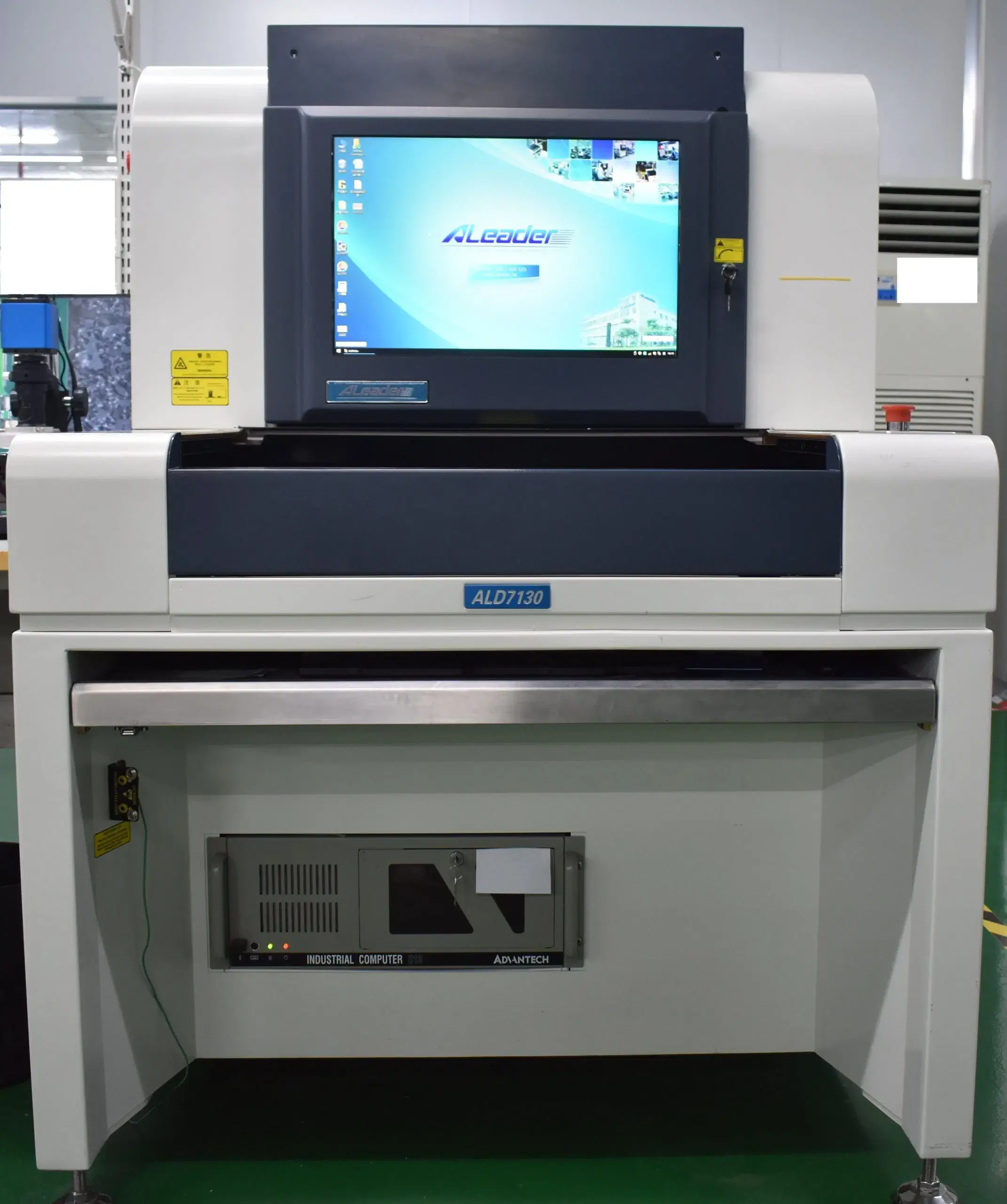
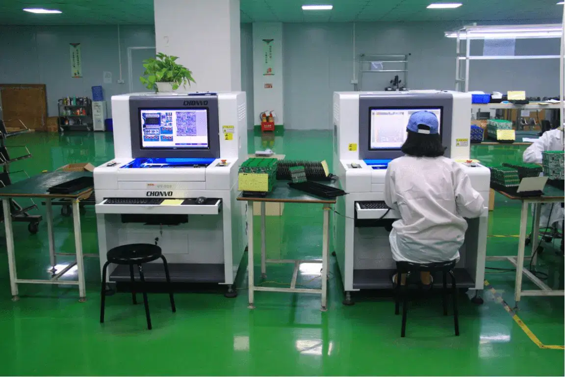
| 3D AOI | Component alignment, polarity, visible solder geometry. | Dense SMT and fine-pitch medical boards. | AOI provides fast geometry evidence but cannot see every hidden joint. |
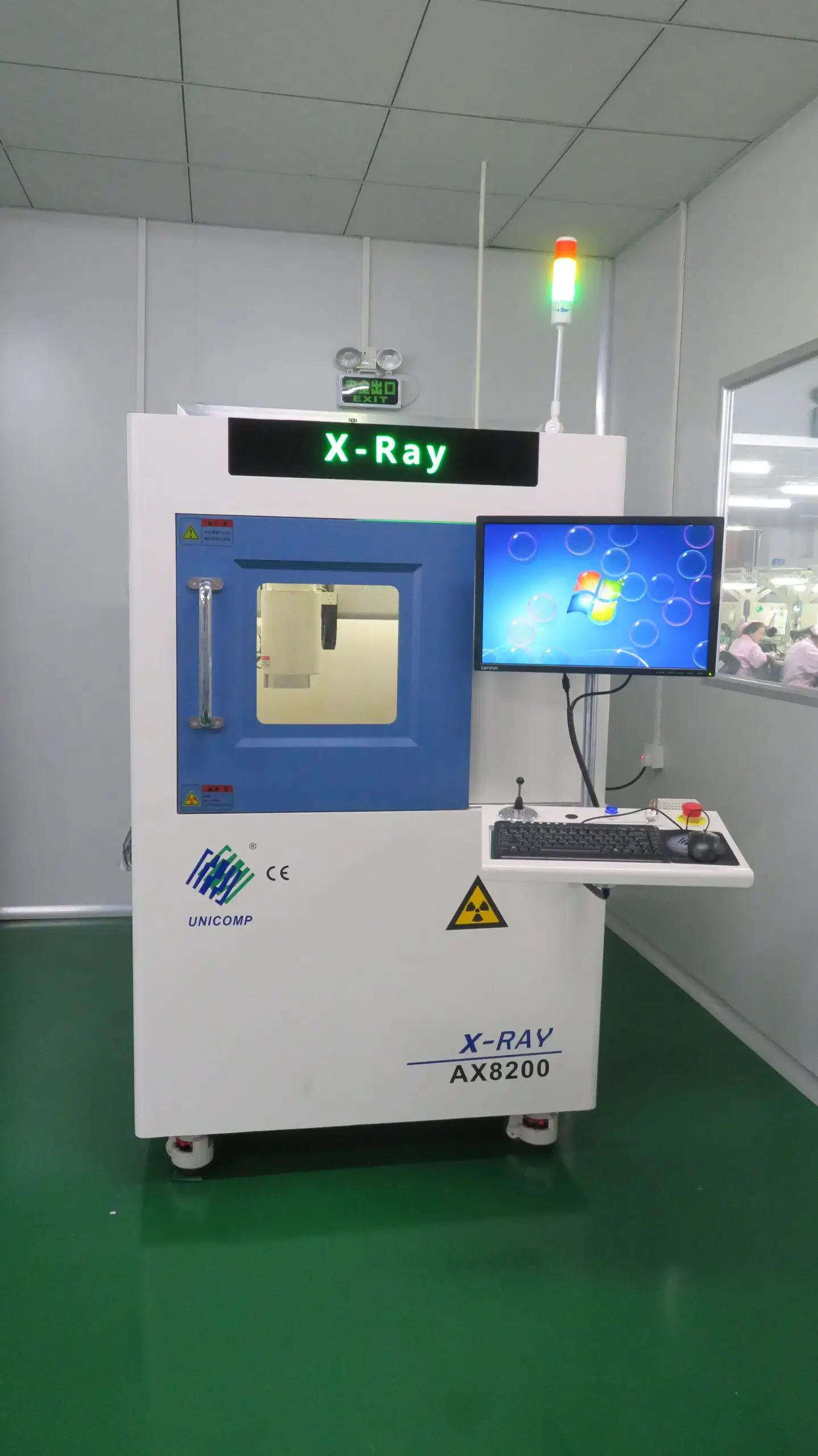
| X-Ray / AXI for BGA/QFN | Hidden solder joints under BGA, QFN, and leadless components. | Boards with hidden or bottom-terminated packages. | Use it where package geometry blocks direct visual inspection. |
| Flying probe or fixture-based testing | Continuity, isolation, and electrical assembly faults. | Prototype and low-volume validation builds. | The result supports verification; it is not a device certification. |
| ICT and TDR probes | Test access and impedance-related verification. | Boards designed with exposed test points and controlled paths. | These methods depend on access designed into the board. |
| ROSE / ionic contamination testing | Residue-driven dendritic growth and long-term reliability risk. | Cleanliness-sensitive medical assemblies. | Data is reported as NaCl equivalent; it flags ionic load, not the specific contaminant. |
| Defect mapping and logs | Repeat defects, assembly drift, and batch-level quality questions. | Prototype, pilot, and production-transfer batches. | Logs give engineering and quality teams a record of recurrence and change. |
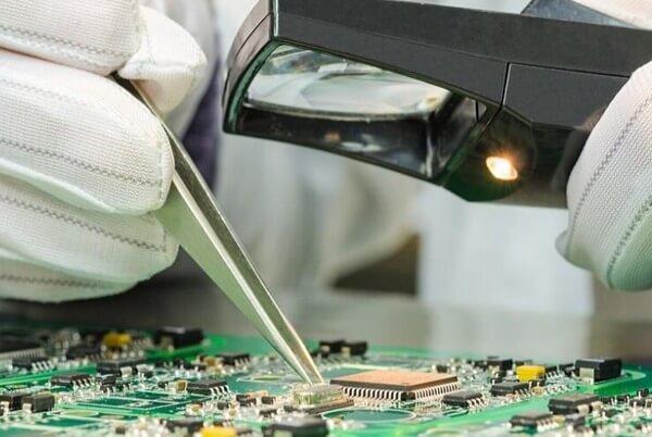
Which Inspection Method Answers Each Risk?
AOI cannot validate the integrity of unexposed BGA joints, and X-Ray will not validate an electrical continuity check.
Assembly Defects That Matter
The PCBA assembly defects that are frequently encountered during medical validation include incorrect polarity, placement that does not match the PCB design, inadequate visible solder geometry, hidden voids or opens within BGA or QFN packages, continuity or isolation faults, and ionic residue. Missing traceability is a different issue: while a PCB may operate as designed, it may not contain the evidence necessary to connect back to it in the future.
Cleanliness Verification
Residue can cause leakage, electrolytic corrosion, dendritic growth, or corrosion around a fine-pitch gap before eventually failing during use. The risk is rarely visible at first power-on; dendritic growth generally needs enough time and moisture to bridge a fine-pitch gap. A PCB that passed functional testing on day one can fail later due to a cleanliness defect that could not be detected because there was insufficient time for the issue to evolve.
Medical Device PCB Applications
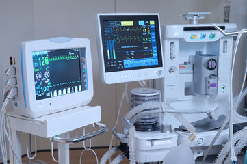
Medical device PCBs must consider the functions performed by the medical device and the implications of a failure if a component of the medical device fails. Imaging, monitoring, therapy, ventilation, infusion, surgical tools, laboratory analysis, and miniaturized devices represent different requirements placed upon placement, signals, connectors, cleanliness, inspection access, and traceability of the PCBs that make up a medical device. Matching the application to the PCB is an engineering question.
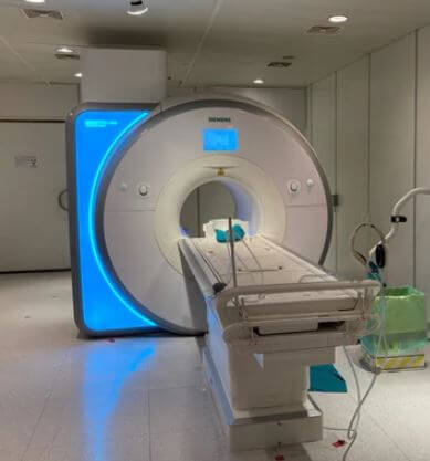
Diagnostic Imaging Equipment PCBs
PCBs in imaging medical equipment are responsible for image capture, power interface control, communication among boards, and signal processing functions within X-ray machines and diagnostic instrumentation. Marginal solder joints or connectors subjected to repeated duty-cycle flexing can introduce intermittent noise into the PCB, manifested as a faint artifact in the image rather than as a hard failure of the PCB. Marginal solder joints or connectors are very difficult to detect in the manufacturing process compared with live scan testing, so connector retention testing and 3D AOI inspection should be used more frequently in the design and assembly of PCBs for diagnostic imaging than on PCBs of similar density that are subjected to a static duty cycle.
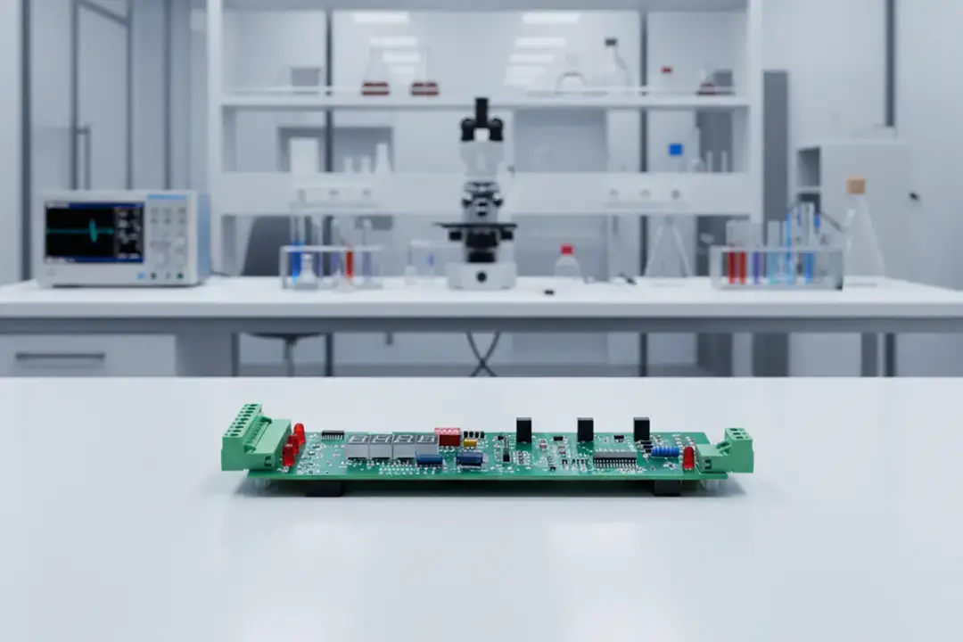
Laboratory Diagnostic Equipment PCBs
PCBs in laboratory diagnostic equipment perform signal acquisition, sample-control electronics, interfaces between analytical equipment, and data processing. For analytical equipment, measurement repeatability relies on stable hardware from batch to batch; in addition to basic function, the assembly of the PCB must be clean and the components consistent with one another. The greatest risk associated with laboratory diagnostic equipment is flux or cleaning residue that may migrate to the optical sensing paths or electrochemical sensors of the PCB. What would be considered cosmetic ionic contamination on a control PCB could be enough to cause instrument drift on a laboratory diagnostic PCB. AOI inspection records, electrical test results, cleanliness test data when required, and batch record data provide insight to the laboratory product team as to whether an instrument problem was introduced during instrument assembly.
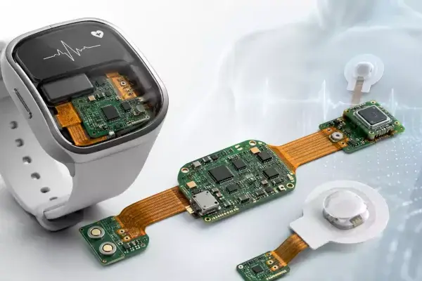
Wearable Medical Device PCBs
Wearable and consumer health care PCBs integrate compact sensing capability, patient monitoring, communication, and battery control functionality. Wearable medical device PCB assemblies generally incorporate flexible interconnects or HDI, which create challenges in board handling and placing extremely small components during PCB assembly. One design flaw concerns the way that electrodes connect to a circuit board or how a battery connector is soldered to a circuit board. When a device flexes, if the flex area is very close to the battery connector, this can create stress on the connector during repeated bending. This is known as a stress crack and is not something that can be detected in a single cycle of bench testing. The device’s design and manufacturing review must also include cyclic flex testing.

Patient Signal Monitoring PCBs
ECG and EEG boards are used for collecting low-level signals from patients via electrodes and connectors, filtering, controlling, and transmitting the low-level signals to the physician. For these PCBs, assembly risk also includes connector location, connector orientation, connector cleanliness, and low-noise pathways. Due to the electrical isolation barrier found on most of these PCBs, the most critical risk associated with the assembly of these PCBs is creepage or clearance around the isolation barrier; for example, a solder bridge created by excess solder or contaminated flux on the isolation barrier could be critical and would cause a dangerous situation for a patient using the medical device, while a solder bridge elsewhere on the PCB may be a minor defect. Beyond connector cleanliness, AOI systems can assist with determining whether connectors are oriented correctly, and isolation barrier verification needs to be included in inspection plans.

Ventilator and Respiratory System PCBs
The design and manufacture of a PCB for a medical ventilator consists of many functions such as monitoring and controlling respiratory parameters, monitoring pressure signals, managing airflow, managing alarms, interfacing with sensors, interfacing with an equipment controller, and sending and receiving information signals to and from other equipment. Since there could be catastrophic results if there are problems with the control board design and its components, assembly inspectors need to view the alarm circuit as a separate inspection area from the main control circuit. Alarm circuits are designed to work through a different circuit path than the main circuit to prevent one solder or component defect from silencing the alarm at the same time it disables control. Inspection records need to be detailed in such a manner that reviewers will be able to verify that both circuits were inspected as separate areas.
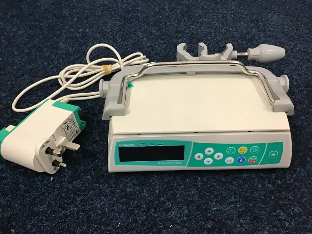
Infusion and Drug Delivery PCBs
For drug delivery, infusion PCBs have a number of elements that need to work together: motor or pump control, sensor feedback, alarm signals, and user interface. For example, a cold solder joint may not cause the motor driver or current-sense circuit to fail, but it may change the amount of delivered volume under load, thus affecting dosing accuracy. Also test the polarity of the motor driver and current-path continuity through dedicated electrical test points.

Surgical Tool Control PCBs
Surgical tools use PCBs for motion control, feedback from the tool, connector routing, and compact control electronics. Hidden-joint inspections and connector durability are challenged by the use of dense SMT and moving harness interfaces. Sterilizable connector interfaces are particularly challenging in this application — the repeated use of autoclave or gas sterilization can loosen a connector or degrade the seal; cycle-tested connector selection and revision traceability have become more important than for a board that has been sterilized once and never reprocessed.
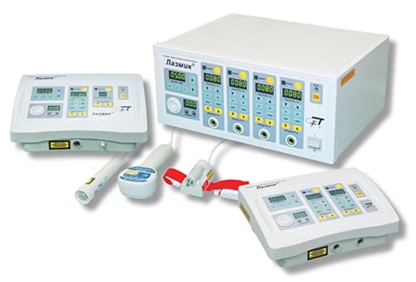
Laser Therapy Control Boards
Laser therapy control boards are responsible for managing the delivery of energy, operating parameters, safety interfaces, and the associated power or control paths. Thermal behavior is the largest design pressure for this application; as heat-sensitive components are close to the optical or power path, they can experience calibration drift with increasing temperature before outright component failure. A thermal-path DFM check of this type of board needs to cover peak temperature and determine the temperature stability across the full treatment cycle of the specific device’s use. Solder-joint inspection, thermal-path DFM notes, electrical checks, and build traceability will provide the engineering team with evidence that the control board was assembled per its expected operating conditions for power and safety interface.
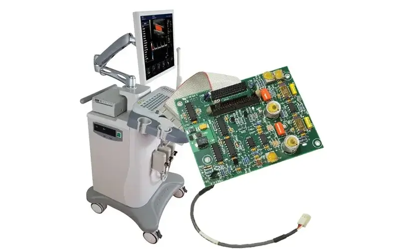
Ultrasound Therapy Control Boards
Ultrasound therapy boards can generate high-frequency signals, control operating parameters for the product, support the transducer interface, and process device feedback; all of these characteristics differ depending on the application. Repeatable performance can be affected by precision control of the paths and placement of components. The transducer interface is the designated pressure point for this type of application; while an impedance mismatch at the transducer connection does not generally lead to an outright fault, it results in a significant reduction in energy transfer efficiency. The routing of the impedance-sensitive components of this board can use the same controlled-impedance stack-up discipline as RF boards, with the design reviewed against the rated impedance for the specific transducer rather than against a generic target.
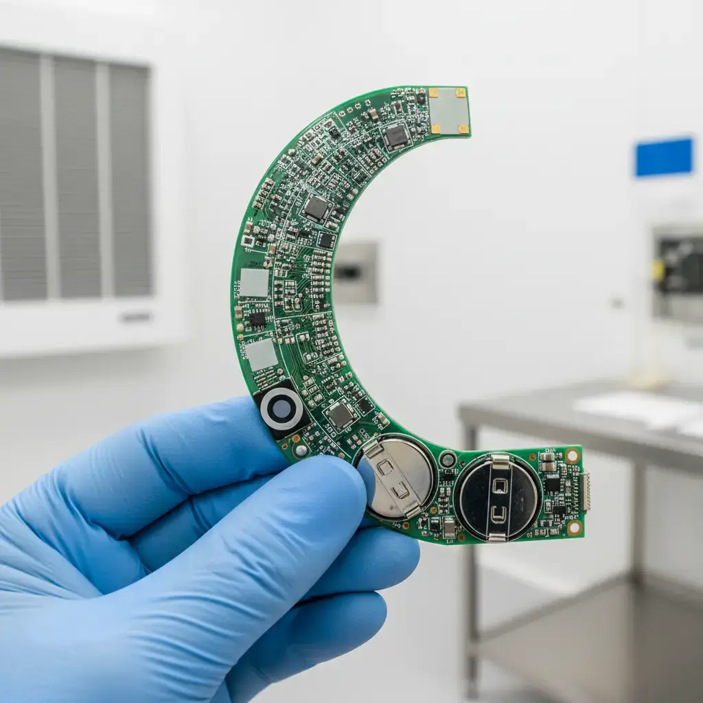
Miniaturized Medical PCBs
The design pressures of implantable-type and miniaturized medical PCBs converge compact sensing or control with very fine-pitch placement, high-density routing, and tightly constrained interconnects, and the design margin of error decreases proportionally. The X-Ray method provides a means for inspecting hidden joint connections; ionic data and material notes can be used where needed to provide assembly evidence. However, as the inspection plan has to be designed in conjunction with the layout, a standard AOI check does not always provide clear sight lines to use for component placement on a tightly constrained assembly.
PCB Types for Medical Devices
Medical device PCBs can be made in rigid, flexible, rigid-flex, HDI, or metal-core constructions that address different constraints of space, motion, thermal load, signal density, inspection requirements, and applicable printed board standards. The total number of layers is only one part of the board selection.
| PCB type | Capability | Device use | Controls | Condition |
|---|---|---|---|---|
| Rigid PCB | 1-64 layers; IPC-6012F requirement; applicable medical addendum requirements when specified for high-reliability medical rigid boards. | Control boards, imaging electronics, laboratory equipment, larger fixed medical devices. | Stack-up stability, connector reliability, inspection access, traceability marking. | A medical board does not need a high layer count unless the circuit density, signal routing, or mechanical design requires it. |
| Flexible PCB | 1-10 layers; IPC-6013E requirement; IPC-6013EM when specified. | Wearables, sensor links, compact patient monitoring, motion-sensitive assemblies. | Bend-zone protection, component placement away from flex stress, clean handling. | Flex construction needs to follow the real bend radius, motion cycle, space limit, and component placement condition. |
| Rigid-Flex PCB | 2-30 layers; rigid, flex, and rigid-flex assemblies; IPC-6013E / IPC-6013EM requirement when specified. | Portable, miniaturized, and space-limited devices that need reliable interconnects. | Controlled transition areas, fine-pitch placement, X-Ray where hidden joints exist. | Device examples show construction choice; they do not imply regulated approval. |
| HDI / microvia | 1+n+1 to 8+n+8; 1.8 mil / 1.8 mil trace and space; blind/buried/via-in-pad/stacked vias; high-aspect-ratio via capability where stackup supports it. | Dense sensor boards, imaging boards, miniaturized medical boards. | Microvia quality, controlled trace/space, via-in-pad planning, inspection strategy. | Microvia diameter and via structure must be confirmed against the actual stackup and via method. |
| Controlled path / lamination | ±5 Ω for single-ended ≤50 Ω; dielectric thickness tolerance ±10%. | Signal-sensitive diagnostic, monitoring, and therapy electronics. | Stack-up stability, impedance-sensitive routing evidence, controlled lamination notes. | An impedance target is meaningful only when tied to the stackup, coupon design, and measurement result. |
| Metal or high-Tg material | FR4 Tg 140/170/180°C; copper core; aluminum core. | Thermal or power-heavy equipment boards. | Thermal path design, solder profile selection, material compatibility. | Cleaning, sterilization, and coating exposure need a separate material review under the actual use condition. |
| Surface finishes and RoHS | HASL, lead-free HASL, immersion tin, immersion silver, ENIG; RoHS-compliant options. | Device-specific finish and compliance needs. | Solderability, storage control, process compatibility, component finish matching. | Finish selection depends on sterilization exposure, shelf-storage condition, solderability window, and component finish. |
| Fine-pitch and BGA assembly | Fine Pitch, BGA and Micro BGA, with 0.3 mm CSP-class pitch and 01005 passive placement within typical process capability. | Compact devices with high pin-count components. | AOI/X-Ray planning, stencil control, solder joint risk management. | Inspection coverage depends on package geometry and joint visibility, not pitch alone. |
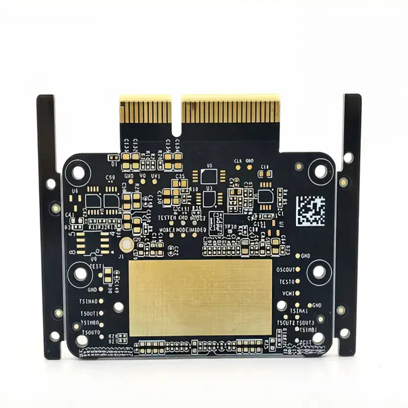
HDI Medical PCB
In the medical field, HDI PCBs are often used in devices where space or interconnect density limits the layout of traditional PCB designs. In these cases, blind vias, buried vias, via-in-pad, and stacked via structures can be combined with dense components; however, each of these via options introduces different risks during the fabrication and assembly. When reviewing the use of microvias created using laser drilling technology, consider the actual stackup. A generic diameter cannot be used to determine compatibility with microvias in a given application; microvia size needs to be contingent on stackup, microvia type, and fabrication control. High-aspect-ratio via capability also depends on the via type, board thickness, stackup, and fabrication control.
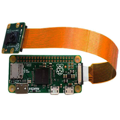
Rigid-Flex Medical PCB
A medical rigid-flex PCB includes component-carrying areas that are rigid, with flexible interconnects that reduce the need for separate connectors in a portable or mechanically constrained assembly. Controlled handling of transition areas, bend areas, and component placement areas is required when assembling rigid-flex PCBs across a flex region. Rigid-flex PCBs only offer packaging advantages to the extent that the mechanical packaging design incorporates an understanding of the rigid-flex construction.
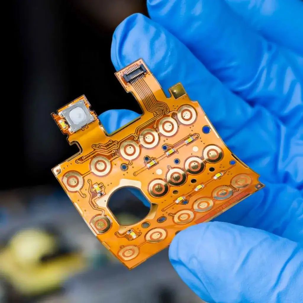
Flexible Medical PCB
A flexible PCB for medical devices is the best solution when designing for wearable or sensor-linked monitoring designs where movement and minimal physical space dictate the interconnect option. When assembling flexible medical PCB assemblies, keep active bend areas clear of any components, protect the flex during assembly, and maintain clean areas around any exposed or fine surface features to avoid contamination.
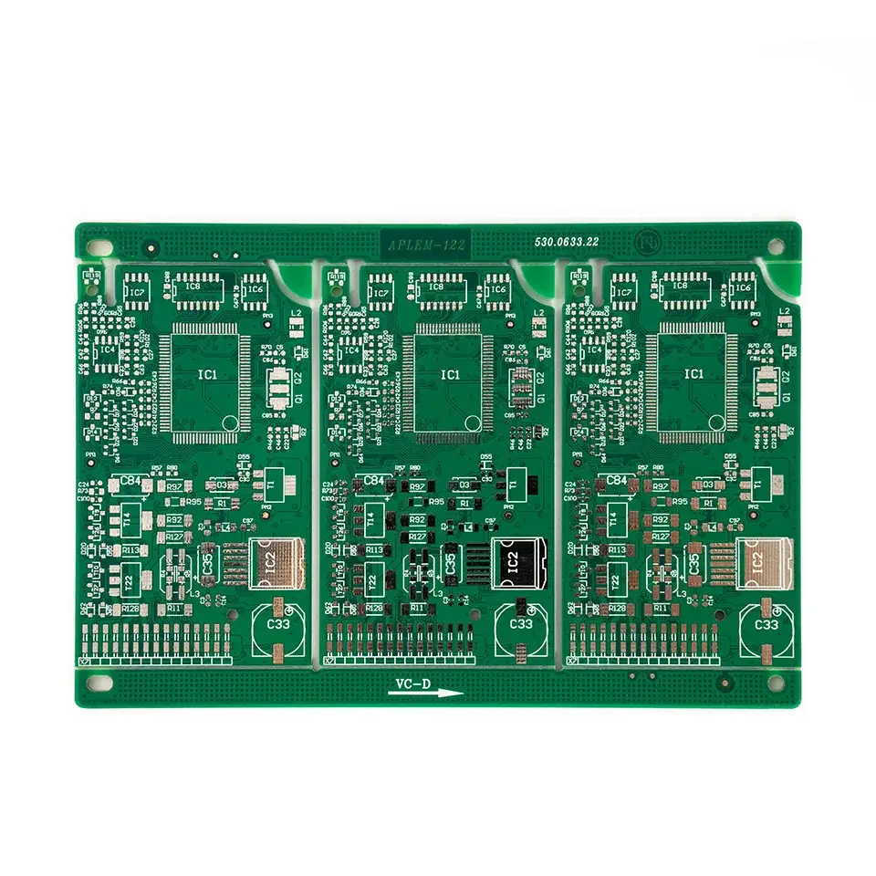
Rigid Medical PCB
Medical rigid PCBs provide the baseline for imaging controls, laboratory equipment, and larger fixed systems. While more extensive connector density, inspection access, stackup stability, and many other factors can make rigid medical PCB assemblies challenging even with a low layer count, these standards are established for the PCB itself, not for the assembly acceptance and soldering practices, which need confirmation through the project specifications.
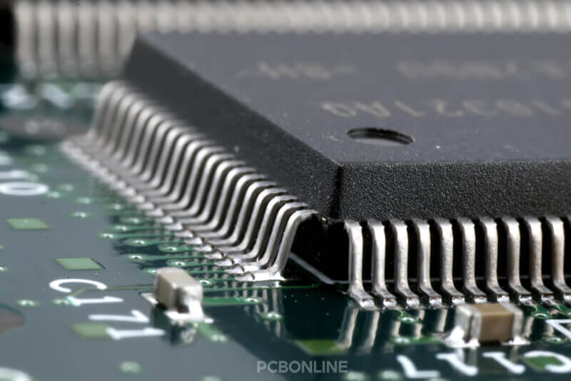
Fine-Pitch Package Assembly
Fine Pitch, BGA, and Micro BGA packages create greater connection density in less space on a PCB. Stencil design, placement accuracy, soldering behavior of the package assembly, and the underlying pad or via-in-pad structures need alignment before the package is inspected. As with any small geometry, small geometric dimensions have less room for process variation.
Design Risks in Medical PCB Assembly
DFM risks in medical PCB assembly start with spacing between components, heat generated, sterilization-compatible materials, access to test points, coating materials, via-in-pad structures, traceability marking, and protection against humidity or ionic contamination. These decisions affect what assembly can control, and what inspection can later confirm.
| DFM item | Medical value | Missed risk | Consequence |
|---|---|---|---|
| Component spacing | ≥0.25 mm spacing for 0.5 mm pitch devices | AOI or X-Ray access may be limited around dense parts. | Use the value as a concrete inspection-access example. |
| Thermal management | thermal vias and 2 to 3 oz copper | High-power medical boards may create local heat stress. | Thermal paths must match the device load and soldering profile. |
| Sterilization-compatible materials | 121°C steam, EtO, gamma; polyimide, PTFE, RO4350B | Material choice may fail the intended cleaning or sterilization environment. | Repeated cycles, not a single exposure, are usually what exposes a marginal material choice. |
| Test access | exposed test points, fiducials, BGA escape routes for ICT/TDR probes | Some defects cannot be checked if access is missing. | Testability must be designed before production, not added after layout is frozen. |
| Coatings | parylene or silicone conformal coatings | Coating selection may affect moisture-sensitive or implantable-type use. | A coating option does not imply regulatory or biocompatibility approval. |
| Via-in-pad structures | plug, cap, and planarize vias in pad | Poor via treatment can cause voids under CSP/QFN devices. | Pad planarity and fill quality affect fine-pitch solder joints. |
| Traceability features | silkscreen fields, lot codes, barcode tracking linked to QMS logs | Identification can fail later quality tracing. | Marking space is part of the design, not an after-build record task. |
| Moisture and ionic protection | dry-pack, coating, and ionic contamination data reported as NaCl equivalent where required | Residue and moisture can create long-term reliability risk. | A dry-pack date without a matching coating or cleanliness record does not confirm the board is protected at first power-on. |
Component Spacing Risk
Spacing between components affects soldering profile control and the capacity for inspecting compact locations. If an object in the vicinity obstructs the sight line of a solder joint, this will hinder access to AOI and X-Ray. The spacing number is a marker for risk but does not represent the only layout rule. The limiting factors for placement of components on a circuit board include package height, pad shape, and density of other components near an area. Design reviews must identify locations where the density of components surrounding a joint will prevent effective validation of a solder joint through established AOI or X-Ray methods. High-power components may use thermal vias and 2 to 3 oz copper to move heat away from the components; the copper thermal mass and distribution for those areas will also influence the solder profile, and assembly must define where local heat control will occur before the final design is confirmed.
Sterilization-Compatible Materials
Material compatibility must be dictated by the appropriate cleaning or sterilization method, and the associated risk will typically be apparent after more than one cycle of cleaning or sterilization. For example, a steam cycle at 121°C generates repeated cycles of thermal and moisture stress to the laminate and solder mask materials; exposure to EtO results in the potential for absorption or off-gassing of chemicals in the laminate, solder mask, and flexible component structures, which have increased exposed surface area; and gamma exposure with accumulated dose during the life of a device can embrittle some polymers or coatings used on or in the device. Polyimide, PTFE, and RO4350B are available material choices, but no single material will provide a complete solution for every device’s reprocessing history. Material validation testing must validate to the number of reprocessing cycles expected for the device.
Test Access Before Production
All planned electrical tests and inspection methods will require a corresponding physical feature to be built into the PCB before assembly; these features cannot be added after the PCB has been manufactured.
Exposed test points let probes used for electrical testing connect to the circuit. Fiducials allow for accurate placement and inspection of the assembly, and BGA escape routes provide access and routing around component packages that are not directly visible.
One failure pattern is a PCB that lists ICT or flying probe testing as part of the test plan, and yet when it was laid out, the corresponding test points were not designed in. This gap in the PCB design is typically found at the NPI and not at the design review because the test points are difficult to see on the schematic but are very evident when the fixture for testing is first built. It is much more costly to close the gap after tooling has been built than it is to catch the error during DFM.
How Cleaning Affects Coating Risk
Coatings will not clean a PCB; they will seal in the cleanliness issues. If ionic residues below the conformal coating were not removed prior to the application of the coating, the ionic residue can create a delay in detecting failures: the accumulation of moisture under a pinhole or the separation of an unbonded edge will create a hidden reservoir where dendritic growth can continue without ever being seen by routine inspection. Cleaning and coating procedures need validation together, not separately.
Via-in-pad structures present a different but related risk. Insufficiently filled or poorly planarized via-in-pad structures can cause solder to escape during assembly, but due to the lack of visibility of the void during inspection, the issue may not be discovered until the electrical tests are performed. Traceability markings also need to be designed with the cleaned and coated PCBs in the same design run.
Prototype to Production Transfer
The medical PCBA build moves through prototype PCBA, validation evidence, pilot-batch feedback, and controlled production transfer. Commercial order steps alone do not prove readiness; the transition to a production-ready PCB requires controls that can reproduce the approved result.
What Should Prototype Assembly Prove?
The prototype assembly demonstrates proper data correlation, correct component placement, proper solder bonding, accessibility for visual inspection, and documentation. A quick-turn medical PCBA will still require the same risk-matched evidence as any other type of quick-turn production; when the design requires AOI, X-Ray, electrical data, or cleanliness data, these data will not be replaced with quick-turn practices.
The pilot-batch production will identify issues with the first boards prior to the first commercial order. Issues include inspection blockages due to package geometry, unavailable component substitutions, unstable handling, or revisions that do not match each other. Rapid prototyping becomes validation of design instead of rushing to ship a sample.

NPI Batch Transfer
NPI turns learning from prototypes into usable repeatable assembly methods. The pilot needs to demonstrate which controls hold steady despite changes to volume, tooling, and line conditions.
When Is Production Transfer Ready?
An assembly method, inspection criteria, revision, and traceability records must be established and maintained before production transfer can begin. Expectations for batches must be defined clearly so that operators, engineering, and quality can review the same released condition.
How to Choose a Medical PCB Manufacturer
When comparing medical PCB manufacturers, base your decision on manufacturing standards, traceability, inspection evidence, capability for board type, application correspondence, production transfer, supply chain capability, and ability to document manufacturing capacity. Marketing statements are weak substantiation of the supplier’s ability unless the supplier connects the marketing statement to a board, assembly record, or inspection record.
Which Supplier Evidence Matters?
In selecting a medical device PCB assembly manufacturer, the manufacturer must provide evidence demonstrating how ISO 13485:2016 controls are applied to the assembly record for that medical device. If the project specifies high-reliability requirements, the manufacturer shall also connect IPC-A-610J Class 3 acceptance to IPC J-STD-001J soldering controls. The focus is whether the records produced conform with the risk of the project.
The inspection evidence must be matched against the board risk and include 3D AOI, X-Ray/AXI, flying probe, ICT/TDR, and ROSE or ionic contamination data when applicable to the build. The construction of a PCB is a good indication of whether a supplier has the capabilities required to build the product being designed, but the supplier can still be missing some of the necessary handling or fabrication controls required to create a working PCB for the device being manufactured. Compare the actual built PCB with the layer count, layer thickness, trace spacing, and PCB type listed in the comparison table rather than a general supplier equipment list.
Also consider the supply chain behind the assembly line, and understand how deep the PCB supplier’s supply chain goes, because component support is easily promised to a customer, but when a component is out of stock, it can be very difficult for a PCB supplier to provide replacement components or requalify alternate parts when it is 2 weeks away from pilot build. PCB suppliers that are able to build a product from bare board fabrication through component qualification to assembly and box build typically have much greater flexibility when faced with component shortages, and normally can replace or requalify alternate sources for parts without having to go outside their own accountable supply chain.
Red Flags Before Selection
Lists of test equipment that are not related to visible joints, hidden joints, electrical faults, or risk of residue are also weak. Look for the lack of a board type match against the prototype learning through the production transfer, along with any claims regarding speed, which cannot be verified through assembly records. Customer reviews and claims by global brands can add context to claims of quality, but they are not sufficient for documentation of manufacturing quality. When evaluating a medical device PCB manufacturer, the claims of quality need testable quality through documentation of inspection outputs and capabilities specific to construction.
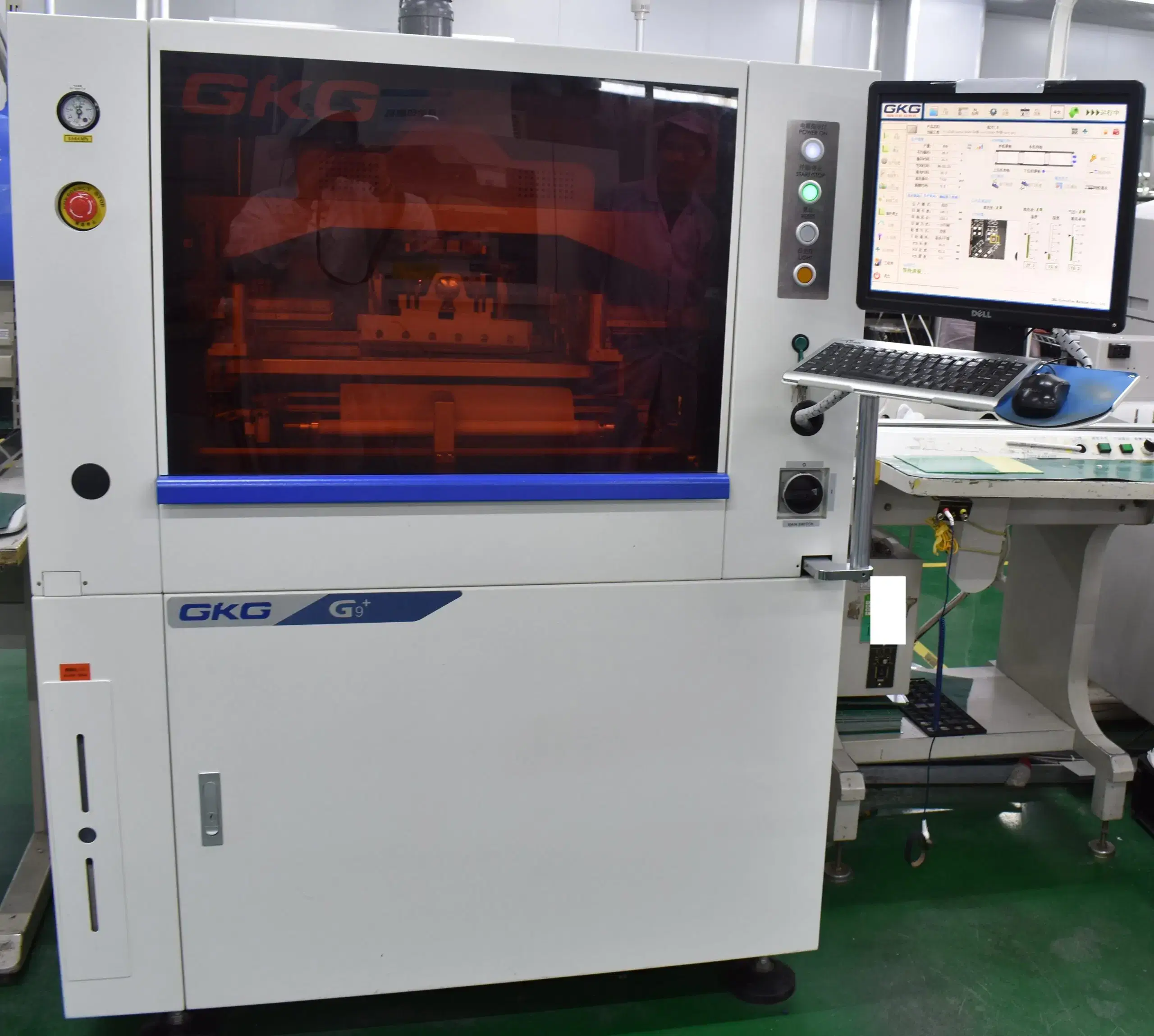
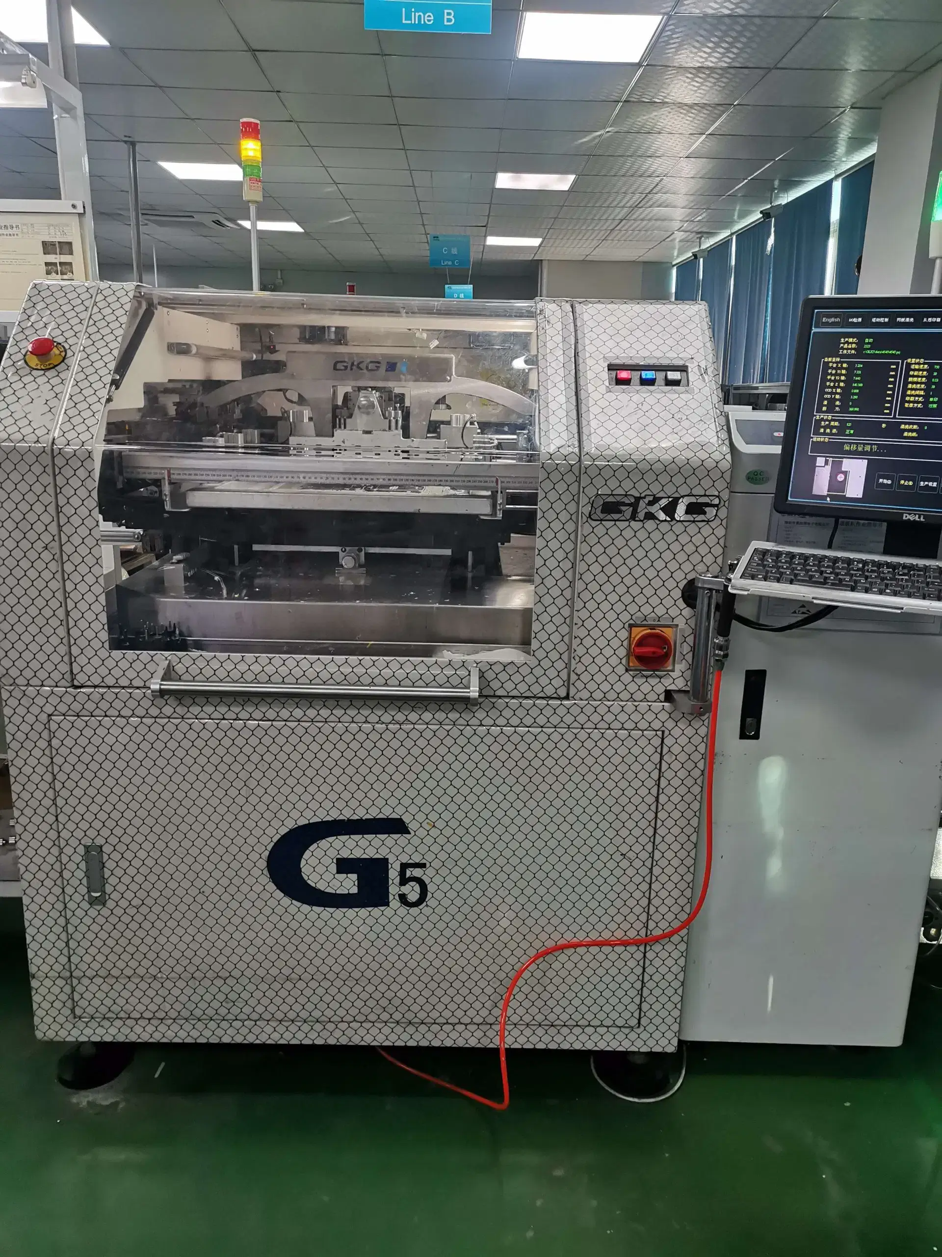
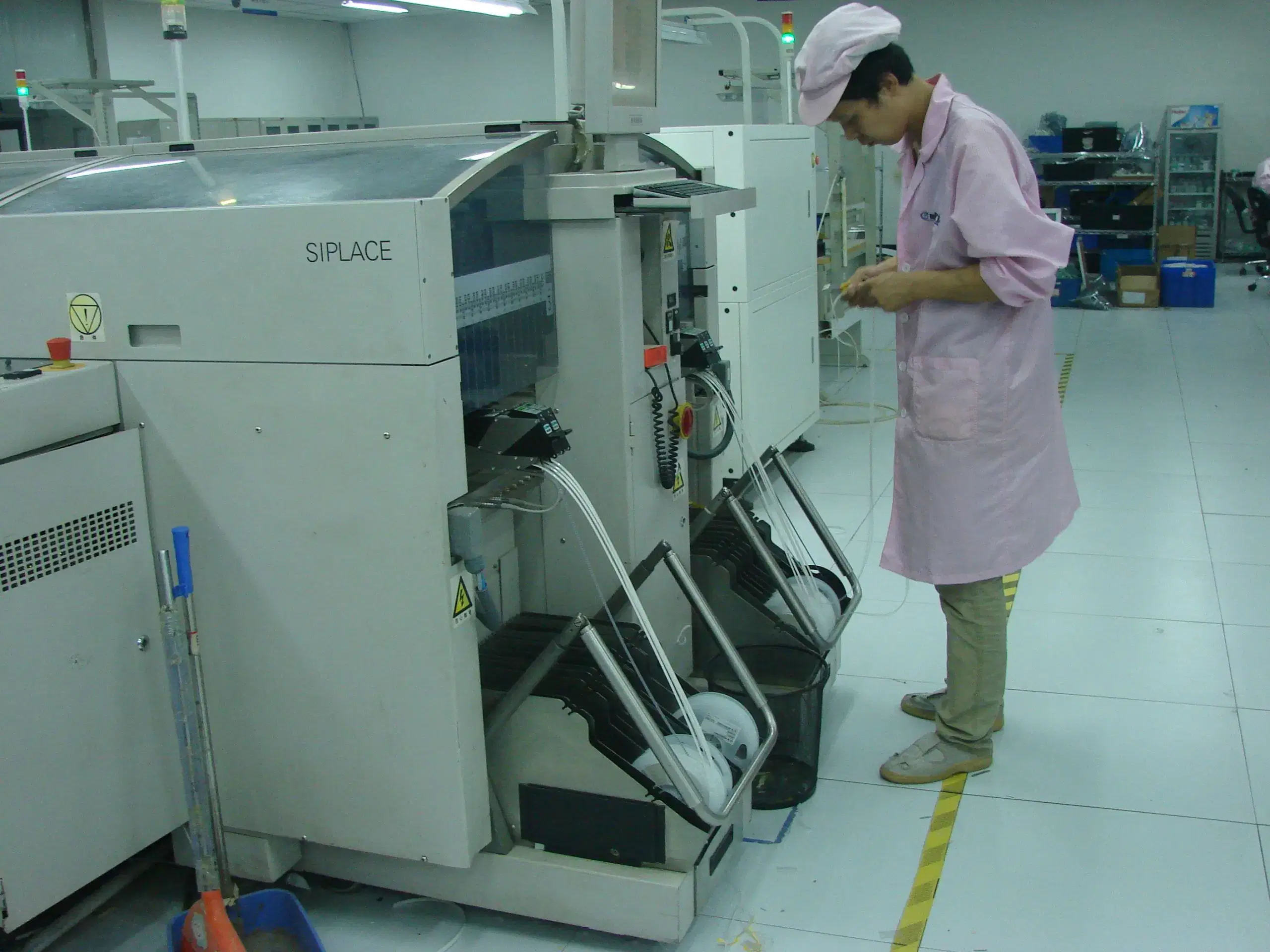
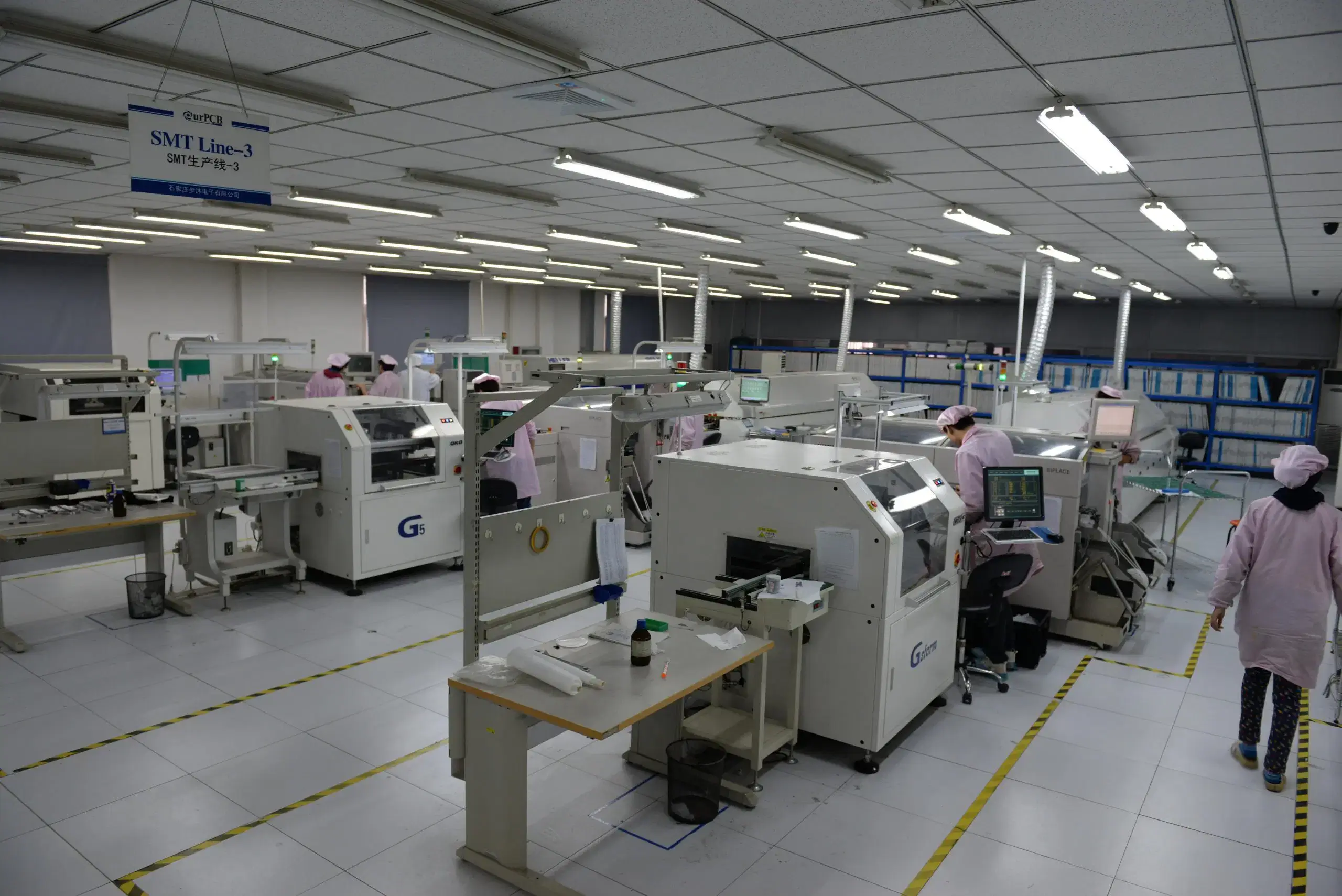
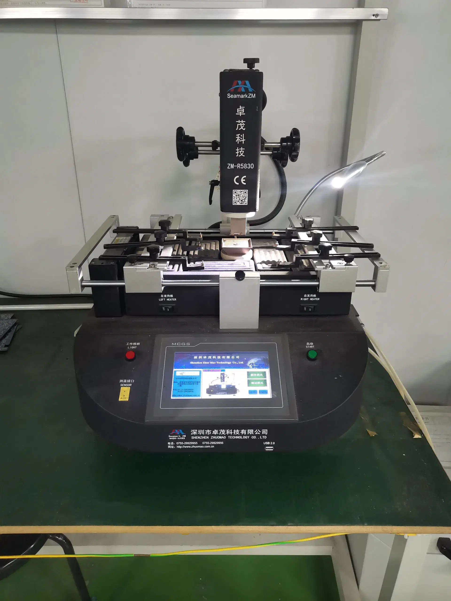
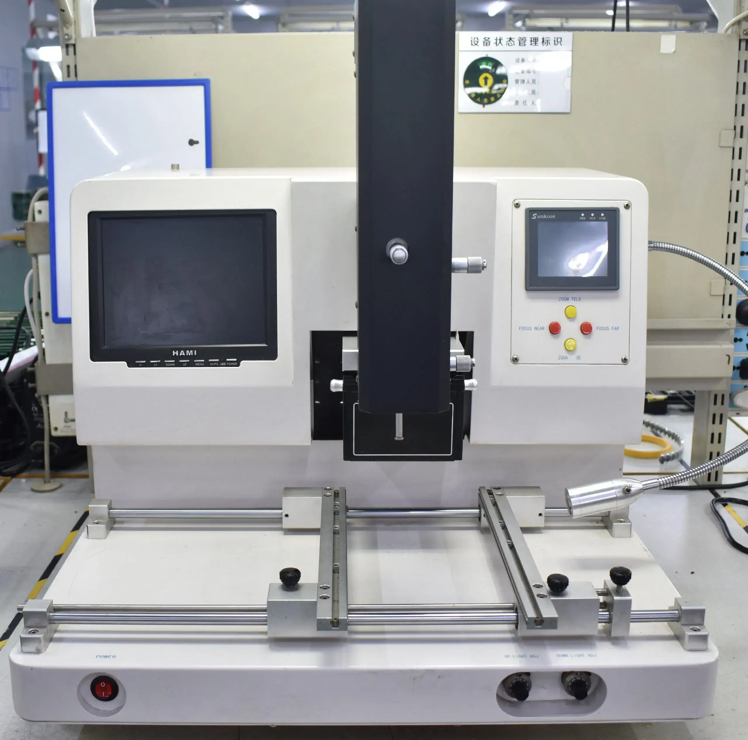
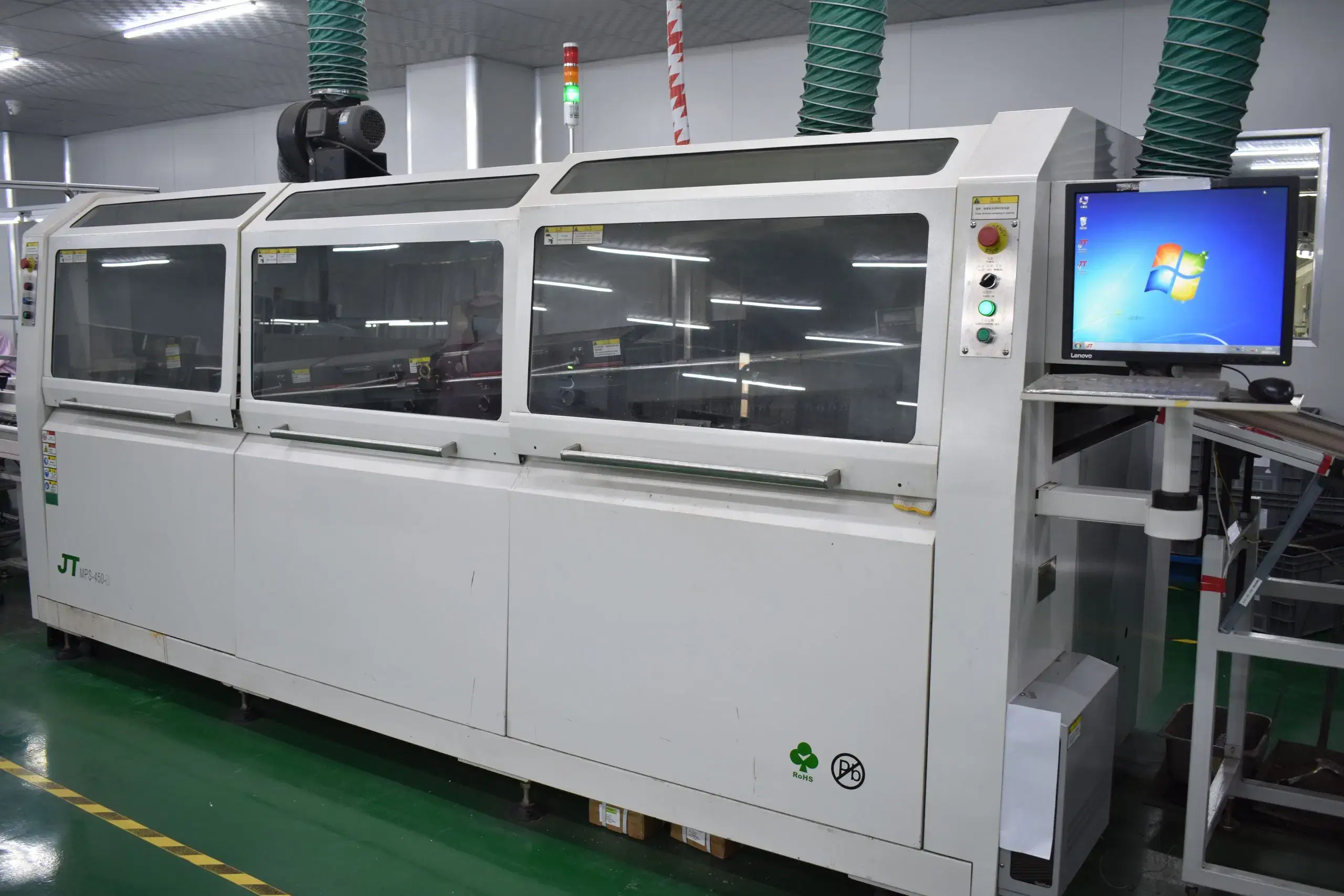
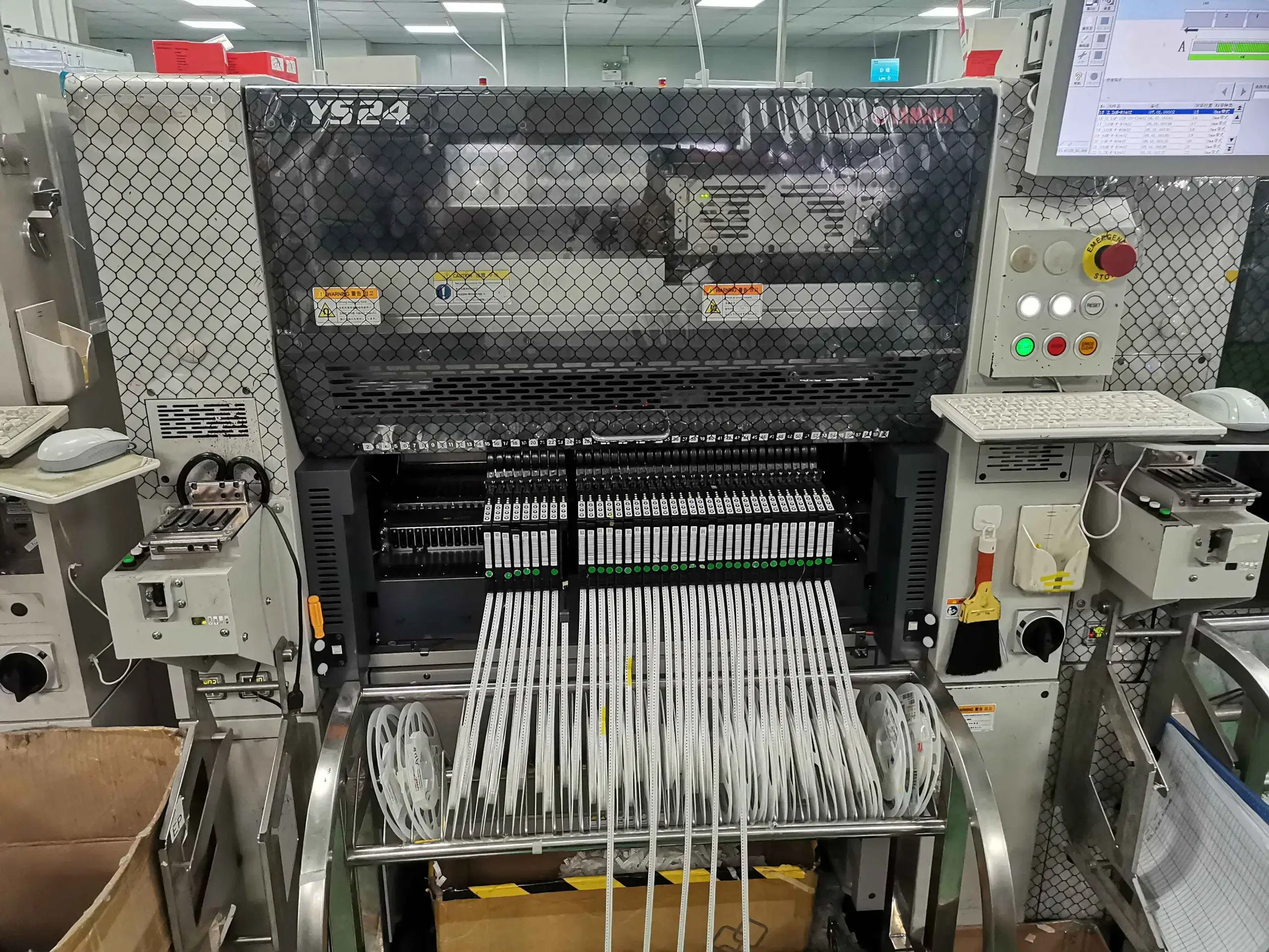
Our PCB Factory Gallery



Frequently Asked Questions
PCB manufacturing is the process of producing a bare printed board, while PCB assembly is the process of placing, soldering, inspecting, and documenting components onto the bare PCB. For most medical device projects, customers will coordinate the two, although decisions concerning the assembly will primarily be based upon the populated board and specifications for assembling it.
The primary standard for medical device quality systems is ISO 13485:2016, while IPC-A-610J Class 3 and IPC J-STD-001J may define acceptance of assembled boards and soldering controls when specified by the customer. IPC-6012F with applicable medical addendum requirements and IPC-6013E/IPC-6013EM set rigid or flex board requirements where applicable.
IPC-A-610J Class 3 will typically be used when building high-reliability assemblies that require stricter acceptance criteria due to the risk of device failure or customer requirements, but the level of risk associated with the device and the customer requirements will determine which class is applicable.
Traceability enables the physical connection of the component lot and serial number to the board batch, build revision, assembly record, and inspection output for that board. The quality team needs to verify that the documentation and records associated with the production window of a physical board correspond to the final build of the PCB.
Medical PCB assemblies can support both prototypes and production batches when prototype inspection, documentation, and results from piloting are all part of one controlled transfer to production. If a customer orders 1 PCB, the same controls may also need to transfer to 10,000 PCBs. In this case, there is no MOQ based on structural considerations of a PCB that would dictate the price of an individual PCB or the length of time to produce it.
To determine which medical PCB manufacturer provides the best services, buyers should compare ISO 13485 evidence, applicable IPC specifications, inspection coverage, board type matches, traceability, supply chain depth, and the prototype-to-production transfer. Although factors such as facilities, experience, and capability to produce multiple product families can be helpful in making comparisons, the best evidence comes from documentation of assembly and inspection records for multiple product families produced by the same manufacturer.
MOQ is determined based upon PCB complexity, component availability, inspection requirements, and whether the build in question is a prototype, pilot, or production batch. A useful planning question for customers is whether the chosen controls and documentation can be applied across all volumes ordered.