Upload BOM & Gerber
-
Mobile: +86 13312967631
-
Email: sales@sugaintl.com

What Is Embedded Components PCB?
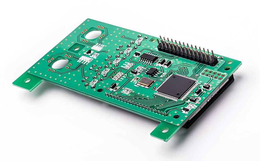
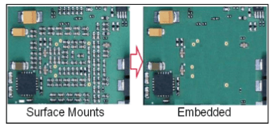
An embedded components PCB combines selected passive or active components within the layers, cavities, and materials of the PCB, in contrast to soldering components to the surface of the PCB. When a design's performance requirements include a reduced surface area footprint, a shorter distance between interconnects, improvements to PDN behavior, improvement in SI, mechanical protection for a passive device, or a more controlled path for heat dissipation, then it may be appropriate to create an embedded PCB rather than using a traditional surface-mount PCB.
Embedded Components PCB Meaning
The term "embedded" refers to the insertion of electrical or thermal functions inside the body of the PCB. Embedded resistors, capacitors, and inductors can be produced with existing materials or manufactured as tiny discrete components. Active devices can be placed within the cavities of the PCB laminate or within laminate-type substrates, where the need to decrease height, increase routing density, or protect the module drives the design of the embedded PCB.
HDI PCBs, cavity PCBs, and copper coin PDN PCBs can support the production of embedded component PCBs, but they are not the same as embedded component PCBs. HDI is used to increase the routing density of a given PCB or to access microvia-type contacts. Cavity-type PCBs create space for the body of the embedded device, and copper coin technology transfers thermal energy from the PCB to the cooling source. The term "embedded component" refers to the electrical or thermal function located within the laminate of the PCB.
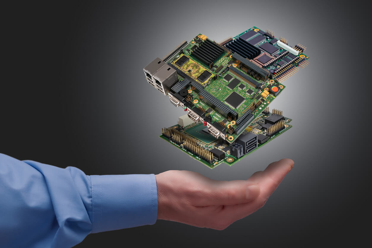
The most important question involves determining what electrical or thermal function will be placed or formed inside the PCB laminate before lamination of the PCB.
Embedded PCB vs Surface-Mount PCB
Surface-mount PCBs are designed to provide a means to access the components mounted on the surface of the PCB. This mounting method is less complicated than using embedded PCBs, because surface-mount component mounting involves soldering the components to the surface of the PCB rather than placing selected functions inside the stack. Surface-mount PCBs are still a valid option for many BOM designs as long as the component placement will not change, or if standard resistor, capacitor, and inductor placement will be sufficient.
Embedded PCBs allow selected functions to be placed within the stack. This can free surface area, reduce the length of local interconnections, protect the passive network, reduce parasitic effects, and create a more robust thermal path between layers of PCBs. By placing dense R/C networks into the stack, the physical footprint on the surface will be reduced, but how much depends on various factors such as layer count, component types, and how many of those networks have real potential for embedding when referencing the percentage. If none of that applies to the design of the PCB, then SMT provides a cleaner solution — therefore the board-level problem should determine the best decision regarding embedded components on PCBs, rather than purely an interest in implementing more advanced manufacturing processes.
| Term | Meaning | Trigger |
|---|---|---|
| Embedded components PCB | Passive or active parts are placed or formed inside PCB layers, cavities, or material stacks. | Surface area, short interconnect, PDN, SI, protection, or thermal path is the design driver. |
| Embedded passive components | Resistors, capacitors, and inductors are formed or placed inside the PCB. | Dense R/C networks, PDN decoupling, RF matching, embedded resistor foils, or spiral inductors. |
| Embedded active components | ICs, bare dies, or packaged parts are mounted in cavities, substrates, or microvia-supported structures. | Compact modules, sensor dies, SiP-like structures, high-density active integration. |
| Copper coin / copper slug | Copper mass is buried or embedded to spread heat. | Compact high-current or high-power heat paths need more than thermal vias alone. |
| HDI with embedded components | HDI stackup, blind/buried vias, fine lines, and embedded structures work together. | Routing density around hidden components becomes the constraint. |
Embedded Passive And Active Components
The PCB components embedded in a PCB may contain many types of components; passive components are typically the most common, with active devices also being present in some PCBs. The various types of passive devices and their corresponding embedding methods are different from those for active devices, as the failure modes differ between the formed resistor layer, the 0201 or 01005 small discrete resistors, the cavity-mounted active device, and the capacitance plane.
Embedded Passive Components
The physical properties of each of these devices will determine what the embedded passive component looks like. The physical configuration for formed and placed passive components is different; formed passive components can contain polymer thick film materials, resistive foil, dielectric layers, etched spirals, or filled materials to create electrical value. Placed passive components require placement control, lamination spacing, and laminate thickness. Resistor networks formed from foil will require a sheet-resistance plan to ensure proper value and a tolerance target for the value.
Embedded Active Components
Embedded active components include ICs, bare dies, sensor dies, or packaged parts placed into cavities or substrate-like designs. In these designs you may use a conductive adhesive, microvia embedding, molding, or flip-chip Au connection depending on the type of device used and the interconnect requirement. The method of active embedding provides a tighter mechanical window. The following parameters of the active device must be established: package height, die attach method, thermal path, pad access, and inspection method before lamination. Do not assume that every IC package can be placed inside a PCB by lamination. Because of access, replacement, or an easier thermal path, some devices will have to stay on the surface of the PCB.
| Type | Examples | Method | Impact | Condition | Evidence |
|---|---|---|---|---|---|
| Formed resistors | Resistor networks, termination resistors | Resistive foil, PTF, ceramic thick film, NiP plating, inkjet PTF | Resistor material layer added to inner core | Best when repeated resistor values justify the material/process layer | Sheet resistance, tolerance target, trimming plan, COA |
| Embedded capacitors | Planar decoupling, capacitance planes, PDN capacitors | Thin dielectric, PTF, CTF, BaTiO3-filled dielectric, 3M ECM | Dielectric thickness and Dk drive capacitance | Best when local PDN or plane capacitance is more valuable than simple SMT replacement | Dk, thickness, capacitance density, voltage stress |
| Embedded inductors | Spiral coils, RF matching, antenna elements | Etched copper spiral, multilayer spiral, ferromagnetic core | Spiral geometry consumes inner-layer area | Geometry and Q factor limit feasibility; not all inductor values are practical | Geometry, line width/spacing, target inductance, simulation model |
| Discrete embedded passives | 0201 / 01005 R/C | Inner-core placement or cavity placement | Component height and lamination clearance must fit inner stack | Good for very small repeatable R/C parts; orientation and clearance must be controlled | Placement accuracy, orientation rules, lamination clearance, X-Ray plan |
| Embedded active devices | ICs, bare dies, sensor dies | Cavity placement, substrate molding, microvia embedding, flip-chip Au connection | Cavity depth and pad connection must be controlled | Requires stronger height, thermal, and test planning | Die attach method, thermal path, X-Ray and electrical test |
| Component molding | Die / wafer-level embedded structure | Dielectric layers and molding | Dielectric layers and molding define the package | Works for die/wafer-level structures when material compatibility allows it | Dielectric system, lamination or molding cycle |
| Thermal inserts (copper coin) | Copper coin, copper slug, heat spreader | Buried copper coin, embedded copper coin, thermal via path | Copper insert changes stackup and heat path | Used when heat path, not electrical value, drives the structure | Coin position, cross-section, thermal simulation, lamination registration |
Embedding Methods And Stackup Choices
Based on several factors, the stackup will depend on which techniques are chosen. For example, the methods of embedding will impact the stackup depending on whether the component is formed, placed, cavity-mounted, or embedded as a buried copper coin.
Inner-Core Component Placement
Whatever location a component will be placed within the final constructed part, it will have an effect on its height, orientation, and clearance, and these attributes are set when the component is placed. Even a small horizontal misalignment will likely only be seen as a hidden defect once the board is assembled and the component cannot be repaired. Minor variances in placement can affect the final product.
Formed Embedded Elements
The stack-up of a formed embedded element is determined by sheet resistance, Dk, thickness of the dielectric, and geometry. The value will be established prior to the manufacturing of the formed embedded element, rather than being determined after production is finished. Materials or processes can change, and once changes are made, the final value may no longer meet the original specifications.
Cavity And Molding Structures
Cavity manufacturing requires a compatible dielectric system, interconnection plan, and lamination window, and these requirements are moved earlier in the production process. Component molding moves closer to substrate-style packaging, where material compatibility and warpage become key questions rather than fit alone.
When Copper Coins Improve The Heat Path
A copper coin embedded or buried in a compact PCB allows for the transfer of heat through internal copper mass. If thermal vias or copper pours cannot create a viable vertical heat path, a copper coin can reduce the length of the heat path between the heated element and the larger heat-spreading area.
Embedded Copper Coin PCB
An embedded copper coin PCB contains a mass of copper located within the structure of the PCB or just below the surface. These types of boards are appropriate for small high-current or high-power areas, where the local heat generated is unable to be distributed via standard copper planes.
Copper coin dimensions, copper coin registration, copper coin lamination fit, void risk level, thermal interface, and electrical isolation must all be thoroughly reviewed. A misaligned copper coin will add complexity to the manufacturing process without providing the expected thermal path.
Buried Copper Coin vs. Embedded Copper Coin
Buried copper coins and embedded copper coins are not interchangeable. There are three main factors that should determine which of the copper coin types to use: where the heat originates from, where the heat will go to, and how much PCB thickness or planarity you can afford to give up in your final product.
Thermal Path Verification
To verify thermal path design, you must conduct thermal simulation, copper insert drawing, via path analysis, coin-to-component alignment review, cross-section verification, void control review, and lamination verification. These checks will ensure that a copper coin does not become a cosmetic feature.
| Structure | Use | Validate | Risk |
|---|---|---|---|
| Buried copper coin | Heat from outer layer moves through vias into internal copper mass | Coin position, via connection, cross-section, voids | Heat path may be indirect if via and coin alignment are weak |
| Embedded copper coin | Copper mass sits inside or under the PCB surface for stronger local heat spreading | Coin dimensions, registration, lamination fit, thermal interface | High copper mass may create lamination or planarity risk |
| Thermal vias | Moderate heat transfer from component pad to inner planes | Via count, via fill, plane connection | Not enough for compact high-current areas |
| Solid copper / copper pour-in | Broad area heat spreading | Copper area, thickness, clearance | Consumes routing area and may not solve vertical heat transfer |
| Heat sink or thermal pad | External or surface-level heat extraction | Mechanical interface, assembly height | May not fit low-profile embedded modules |
Design Rules Before Fabrication
Embedded component checks should occur earlier than standard SMT checks. Once a board has been laminated, it is typically impossible to perform a second set of design checks. These checks have to be completed by the time the stackup is frozen.
DFM Inputs For Embedded PCB
The BOM separates formed embedded components from placed embedded components and surface-mounted components prior to design review; this is essential because mixing together material-formed values, buried bodies, and serviceable surface parts can lead to stackup decisions based upon inaccurate information.
Thermal And Mechanical Simulation
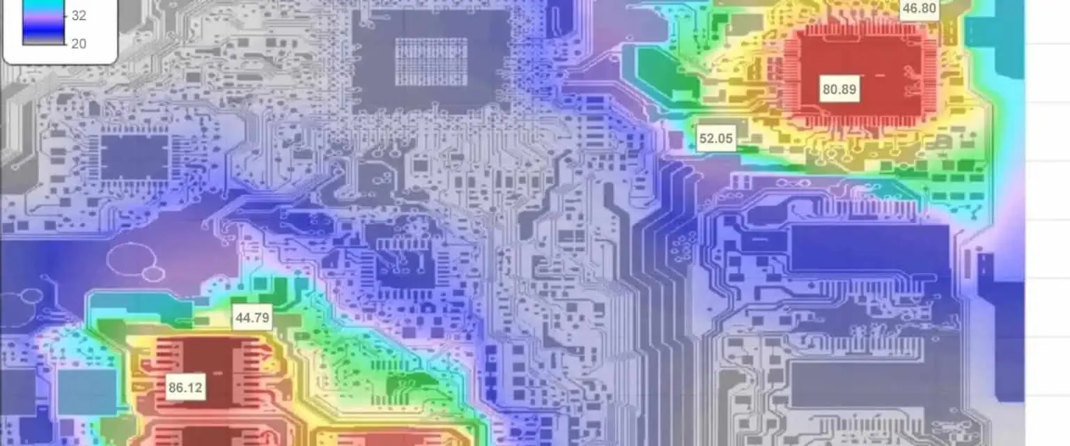
Simulation predicts potential heat paths for copper coins, magnetic components, thin cavities, and warpage-sensitive stackups; basically anywhere a buried structure may move or have no margin to support itself, which will not show up until the lamination process is completed.
Testability And No-Rework Limits
It is essential to design in the necessary value checks, test pads, and X-Ray access for embedded terminals before the board has been laminated, since these items will not be accessible once the board has been produced.
Applications
Embedded passive PCBs provide added value at the PCB level where space, noise, PDN performance, heat transfer performance, reliability, or module height is the constraint.
Wearable Health Monitor PCB
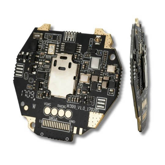
Embedded passives may be employed in a Wearable Health Monitor PCB to reduce the thickness of the module, protect any R/C networks that have been packaged in a repeatable manner, and reduce local paths around sensors, wireless components, or power rails. The mechanical window will depend on the placement of 01005 or 0201 parts and the areas of lamination. Mechanical flexing will put mechanical stress on embedded capacitors and resistors that surface-mounted capacitors and resistors do not encounter in the same way. The bend radius for the product should be verified with the location of the inner cores and their clearance against the board before completing the stackup.
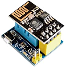
IoT Wireless Sensor Module
The integration of embedded resistors, capacitors, or inductors into the PCB provides an opportunity to shorten the distance of the signal path around the RF front end and matching networks. One of the potential pitfalls of this technology is that a Q-factor change from one batch to another will affect how the matching network resonates but may be undetectable through electrical testing at the board level. Often, the mismatch will be detected once the module is placed into service during integration and not during incoming inspection.
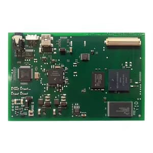
Smartphone Sensor Module PCB
Smartphone camera, biometric, and small sensor modules located on a PCB have very limited surface area for components. The use of embedded passives frees up board area, shortens the distance of local paths, and protects repeated networks inside the small outline of the module. The main limitation of these types of modules is interference between the cavity or embedded passive area and surrounding dense SMT routing, rather than just the cavity's thin stackup space. Design verification must also check the height of the cavity, the placement of 01005 or 0201 components, and the pressure required to laminate against the surrounding dense SMT routing before finalizing the design.
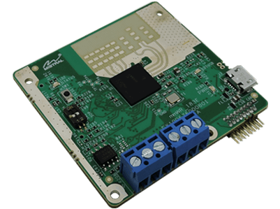
Automotive ADAS Radar Module
An ADAS radar module may utilize embedded passives, controlled RF routing, and HDI interconnects to minimize parasitic paths while maintaining a compact design. The level of dielectric-thickness variance that is acceptable for low-frequency applications will not work in this case: a local variation in the thickness of an embedded capacitor dielectric that is considered a rounding error for audio or digital frequency will become an impedance discontinuity when using millimeter-wave frequency signals. The same component that functions well on a power board may not function correctly when used in a radar stackup, even though there is no defect in the component.
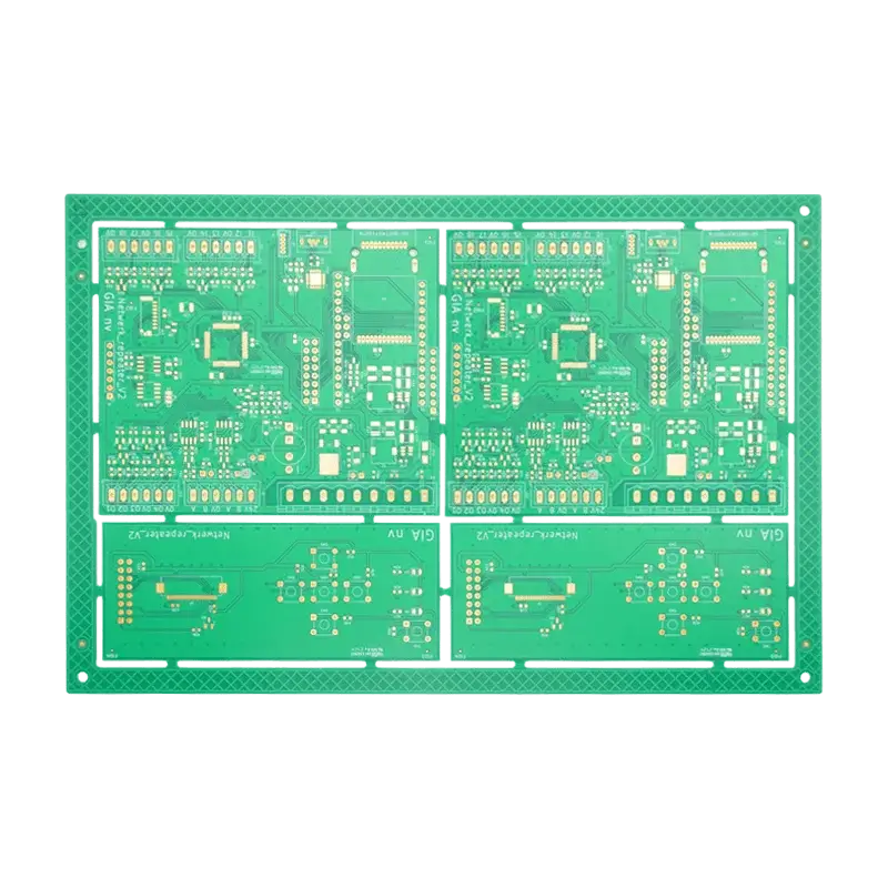
Industrial Control Module
A compact PLC, robot, or industrial instrument may utilize embedded passive components due to vibration resistance, board density, and stable interconnects. The most important consideration for durability is vibration: repeated cyclic loading can damage the formed foil of resistors or loosen 0201/01005 components within the cavity over time. The thermal-mechanical simulation and cross-section sampling methods that have been developed for verification of copper coins and cavity designs should also be suitable to verify the vibration profile of the component.
Medical Diagnostic Sensor Module
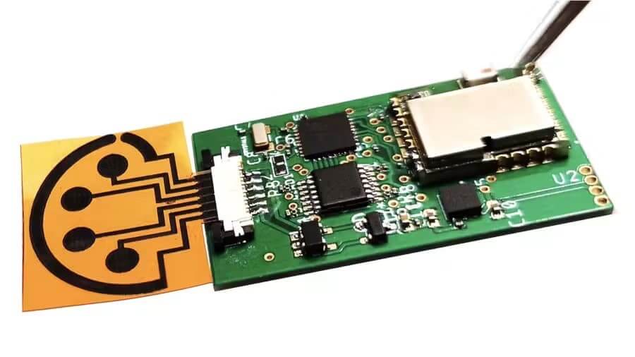
Medical diagnostic sensor modules can utilize embedded components to help protect small passive networks, reduce the size of the module, and keep sensitive signal traces to a minimum. The biggest constraint that is often missed here is recall exposure: when a resistor or capacitor is embedded, it can no longer be removed for retesting as a surface-mounted component can. If in the future there is a concern about the quality of a material lot, the traceability plan must be able to identify affected boards by lot rather than by physically re-inspecting the passive.

Aerospace Control Electronics
Aerospace control electronics may justify embedded structures based on weight savings, the need for compact routing, stable interconnects, and environmental reliability versus ease of rework. The aerospace-specific risk is related to the coefficient of thermal expansion mismatch between the embedded resistor, capacitor plane, or copper coin and the surrounding material stack. Due to thermal cycling, it is possible to develop fine-line delamination around the embedded structure long before it becomes evident by inspection on the outer layers, which is why thermal-mechanical simulation and cross-section sampling are more important in this application than in a ground-based design.
Defense Radar Electronics
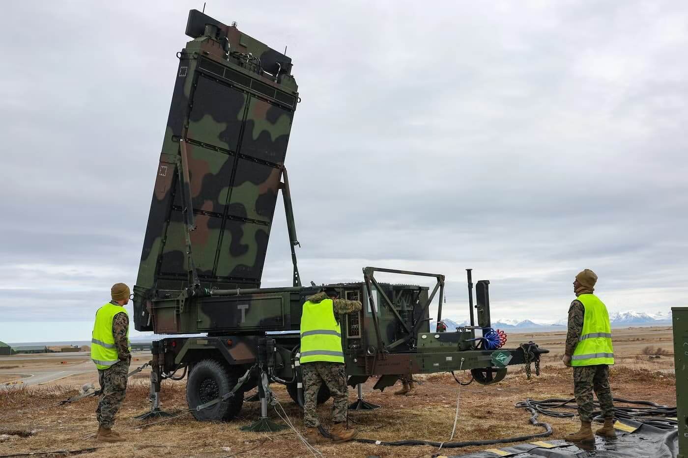
The use of embedded passive devices, fine lines, and RF substrates allows for control of the matching, decreased interconnection length, and compact phased-array layouts. Example structures may involve 12L ROGERS 4003C + Ticer + ECM2012, a 14-layer radar board, 40 µm mSAP, and COA.
5G Beamforming Board
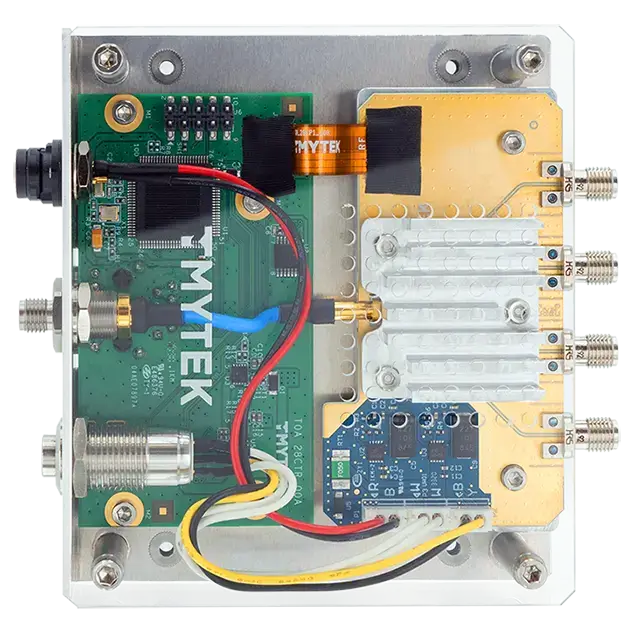
5G beamforming boards employ embedded passives and fine-line RF routing to create a smaller footprint of the matching network and reduce parasitic discontinuities. As the channel count increases, so does the cost of the board; hence, the relevant question is not whether embedding is feasible, but whether the dielectric selection, impedance control, line/space, and passive tolerance can meet the required frequency and cost-per-channel goals.

LEO Satellite Phased Array Module
LEO satellite phased-array modules may use embedded passive structures along with HDI routing to create a compact design that repeats antenna channels. Examples of layouts include 16×16, 8×8, 4×4, and 10×10 phased-array patterns, all requiring similar control over materials, passive tolerance, and fine-line routing. Launch-environment reliability and long-term stability are usually more important to OEMs than unit price.
High-Speed Computing VRM Board
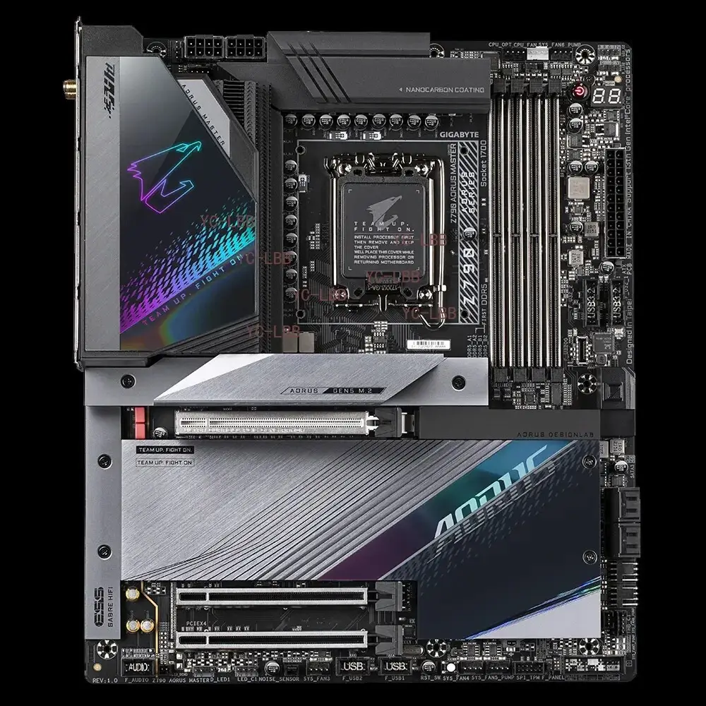
The server VRM or DDR power delivery area employs embedded capacitance planes or embedded passives to achieve low loop inductance and local PDN behavior. The gain from using embedded planes occurs if the embedded plane is electrically placed as close as possible to the switching node. If an embedded capacitance plane is buried under an incorrect layer, then excessive via length between the plane and load can cause most of the inductance reduction previously intended by embedding the capacitance to be lost; therefore, the placement of all planes should be verified against actual current paths and should not just be referenced from a stackup diagram.
Compact Power Supply Control Board
For compact power supply control boards or gate-driver boards, when they have constraints in loop inductance, heat build-up, and board area, this may be addressed by using embedded passives or copper thermal pathways. If an embedded passive is situated adjacent to a copper coin within a high di/dt switching pathway, the coin's return current can couple noise into an adjacent formed inductor or capacitor plane; hence, the proximity of both parts and the reference-plane routing should be evaluated in relation to one another as opposed to treating each as two independent decisions. The methods of thermal simulation, copper coin or copper pour selection, and magnetic component heat limiting will determine if hidden power architecture is viable.
Choose An Embedded PCB Manufacturer
When evaluating an embedded components PCB manufacturer, check material access, types of embedded components, HDI/cavity/copper coin requirements, passive tolerances, inspection methods used, IPC standards applicable, volume fit, and documentation control.
Manufacturer Capability Checklist
Prior to production, SUGA will confirm the embedded component type, material set, tolerance target, HDI/cavity/copper coin requirements, and inspection plan.
Evidence That Reduces Supplier Risk
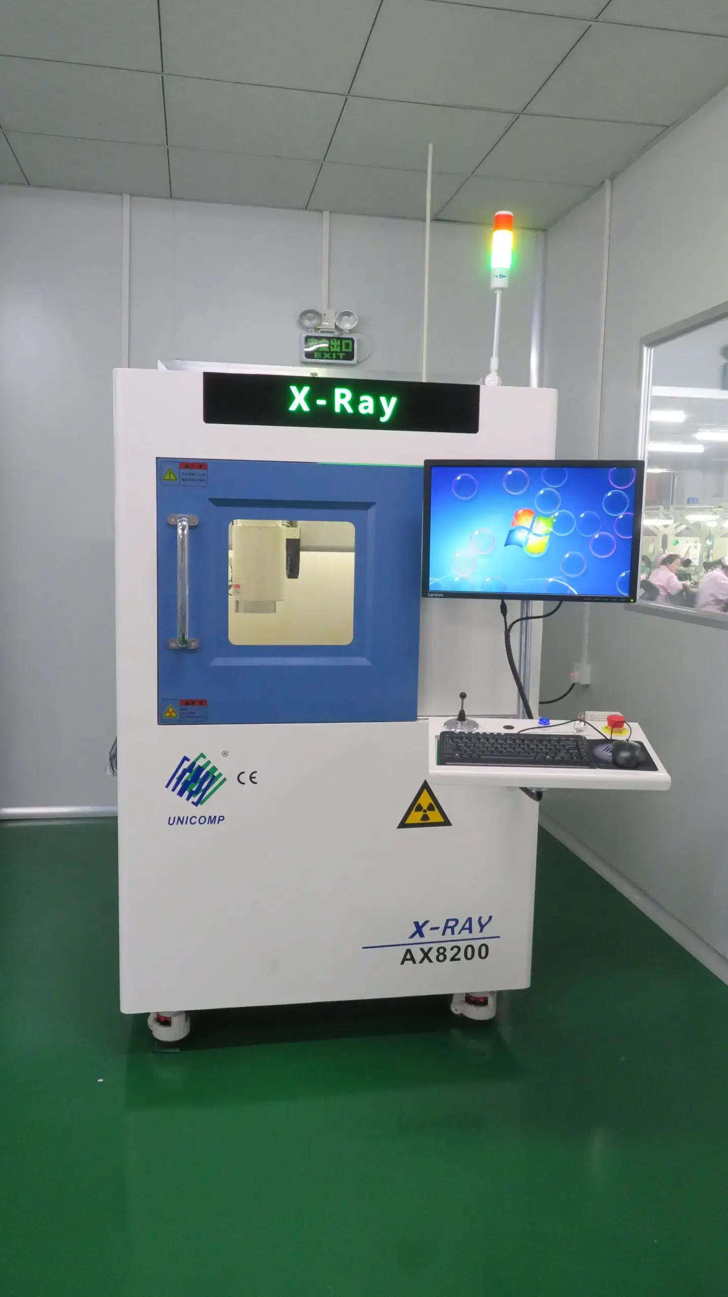
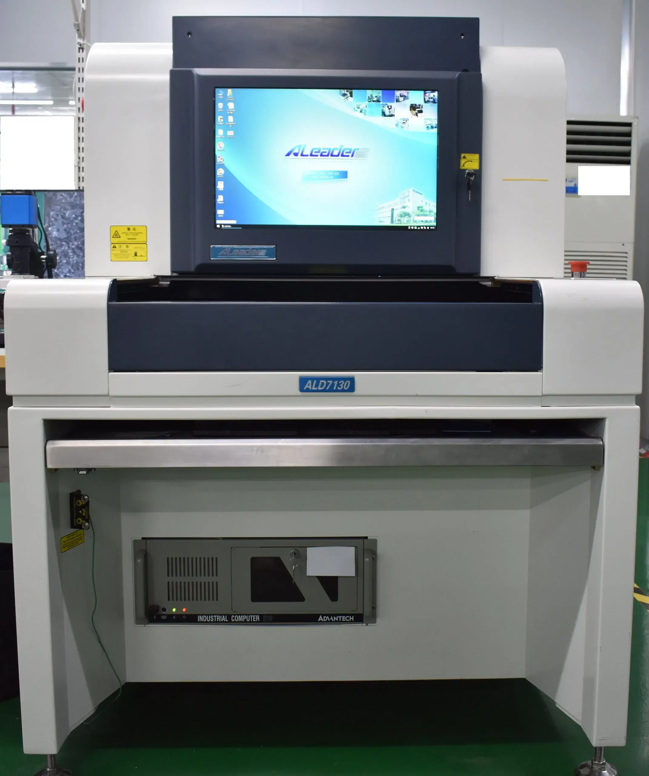
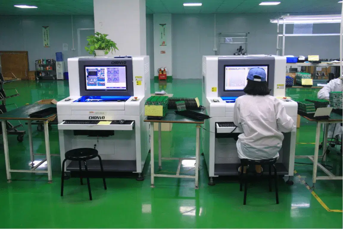
Any risk concerning the material options listed above is reduced when a COA is utilized as verification instead of only a datasheet. IPC-4811 applies to embedded resistor materials, and IPC-4821 applies to embedded capacitor materials. Hidden structure risks can be mitigated through the use of AOI, X-Ray, cross-sectioning, E-test, flying probe, custom test jigs, and 100% electrical testing. This testing will be performed at whatever level of production is necessary for product quality.
IPC-A-600M, IPC-6012F, IPC-6017A, and IPC-7092A define acceptance and implementation requirements. An order of one part or low volume may be technically supported; however, the advantage of a repeatable design and the additional value of formed passives and laser trimming are more economical on a per-part basis.
Manufacturing Control Requirements
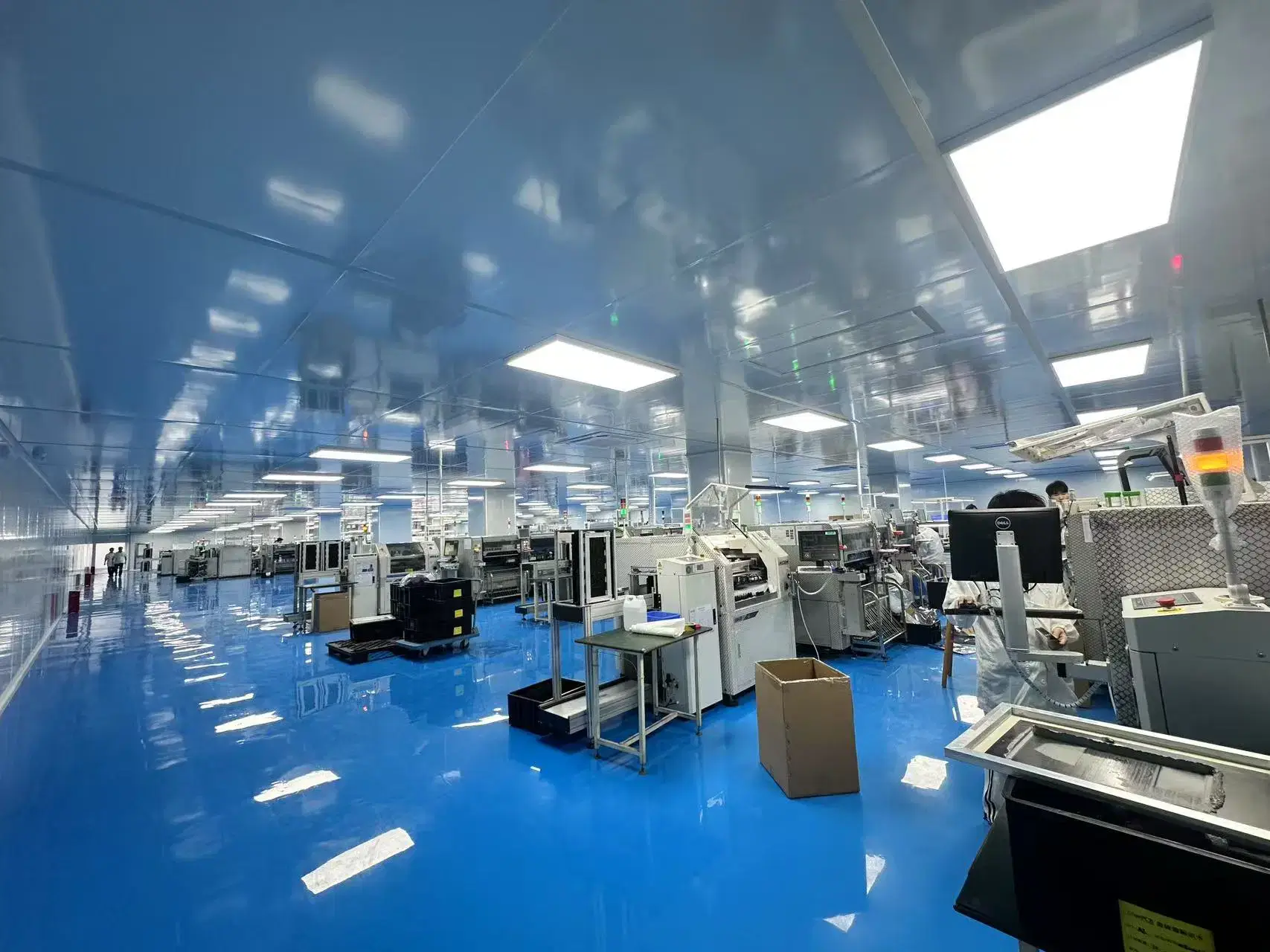
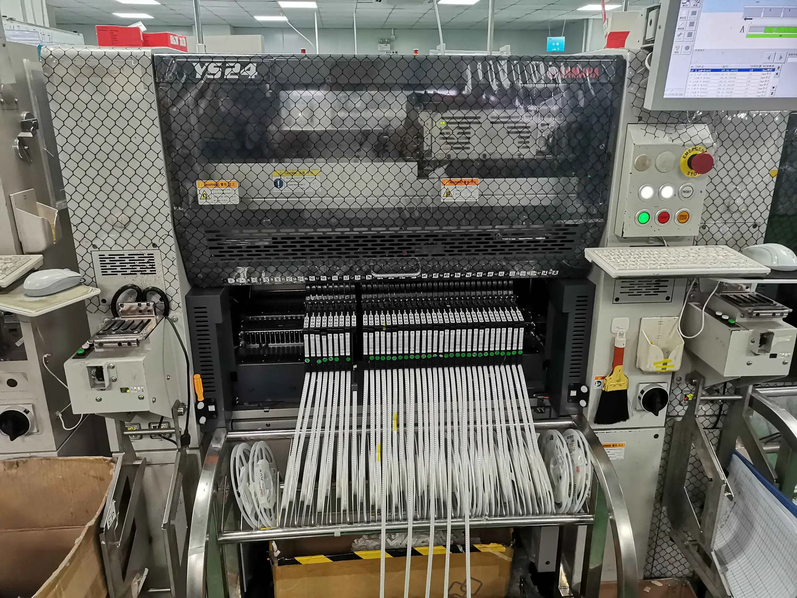
For embedded component PCBs that require specialty materials, mSAP, cavity, copper coin, HDI, X-Ray, or adjacent PCBA capabilities, manufacturing, inspection, and assembly requirements should be aligned before production.
| Criterion | Evidence | Why | Approach |
|---|---|---|---|
| Embedded component type | Formed R/C/L, placed 0201 / 01005, active die, copper coin | Different component types require different process flows and tests | We review formed and placed embedded component PCB requirements before stackup freeze |
| Material support | FR4, High Tg FR4, Reinforced FR4, PTFE, Rogers, Arlon, Taconic, Ticer, FaradFlex, OhmegaPly, 3M ECM | Material substitution can damage SI, PDN, RF, or passive value performance | We confirm material availability and can provide COA when the project requires named materials |
| HDI, cavity, and copper coin | HDI 2/3/4 steps, cavity process, blind/buried vias, copper insert drawing | These decide whether the stackup is manufacturable | We check stackup, cavity, copper coin, and via path before production |
| Passive tolerance | ±10–20%, ±10%, ±5%–±8%, ±5%, ±1% with laser trimming | Tolerance drives cost, process method, and inspection depth | We define achievable tolerance after material and geometry checks |
| Inspection | AOI, E-test, X-Ray, 100% electrical testing, flying probe, custom test jig | Embedded defects are hidden after lamination | We match inspection method to prototype or mass production stage |
| Standards and acceptance | ISO9001, UL, RoHS, IPC-A-600M, IPC-6012F, IPC-6017A, IPC-7092A | Standard alignment reduces your uncertainty | We match documentation and inspection level to the project requirement |
| Volume fit | Low to mid volume, 1 piece, prototype-to-mass-production support | Some embedded passive structures are technically possible but economically weak at low quantity | We explain when embedded passives make sense and when SMT remains better; for early prototypes we often recommend placed 0201/01005 passives as a lower-cost bridge before committing to formed embedded passives at volume |
| Project continuity | Direct factory control, adjacent PCBA capability, and inspection capability | Specialty processes require stable material, inspection, and assembly planning | We align manufacturing, inspection, and PCBA requirements before production |
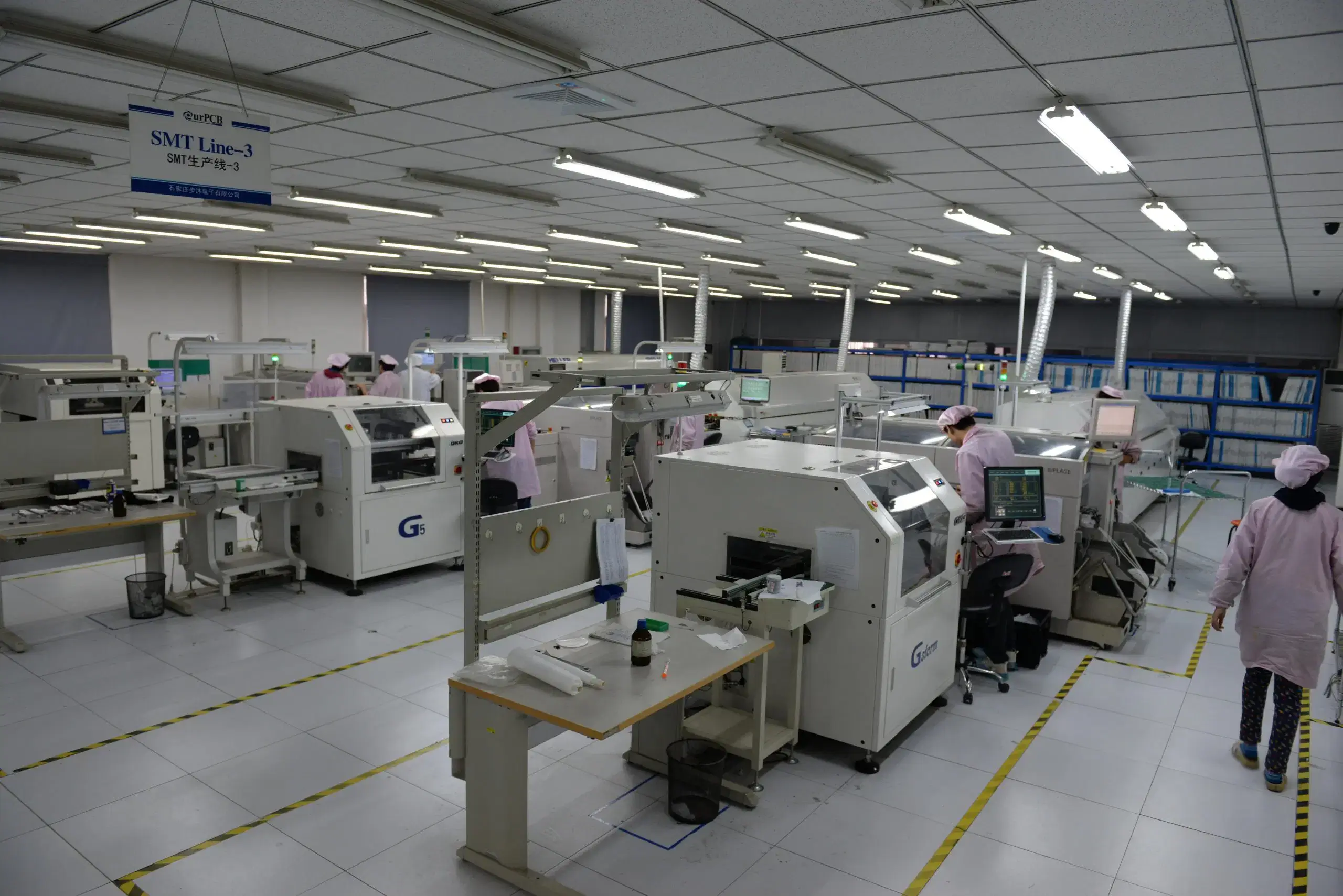
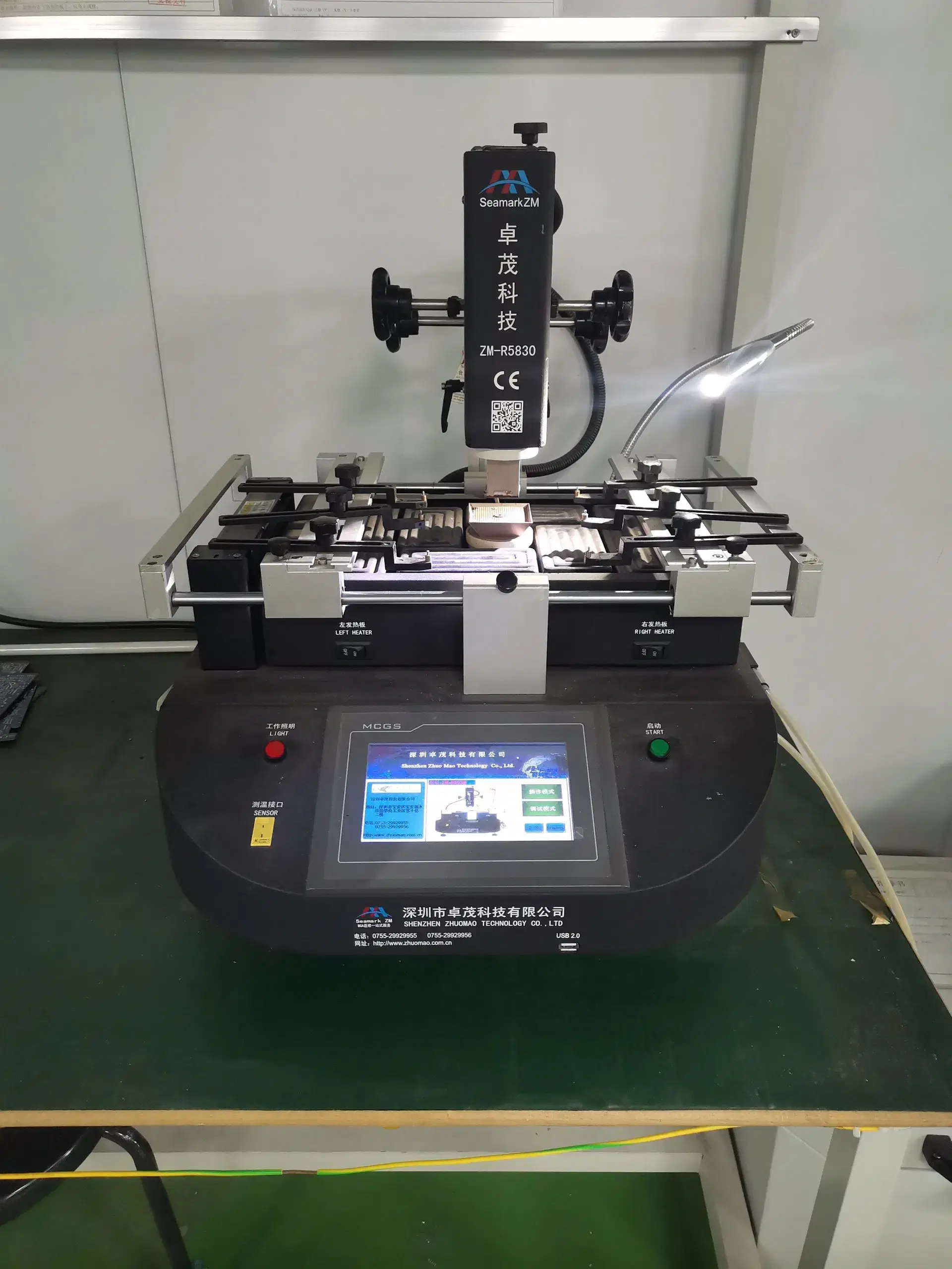
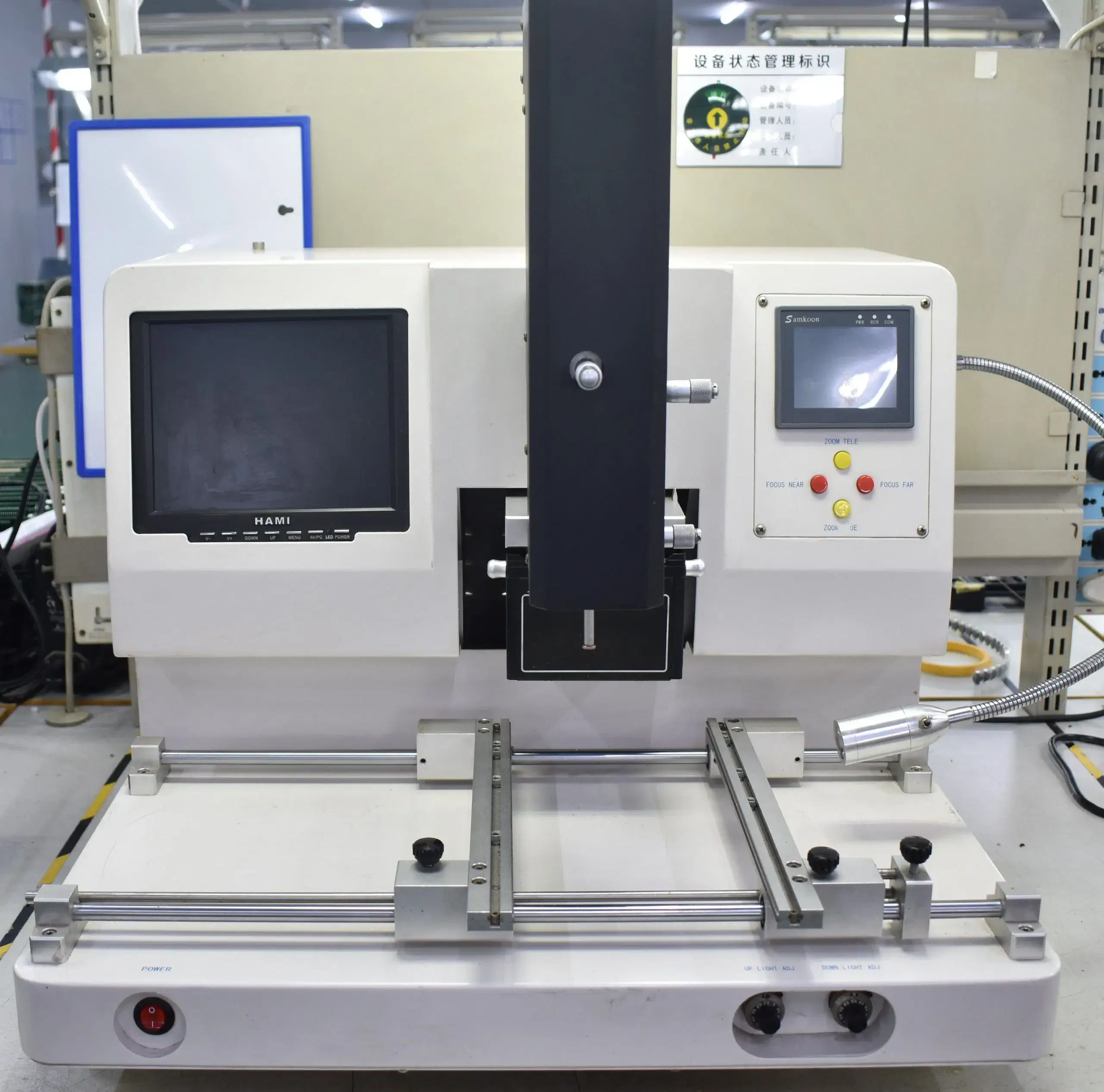
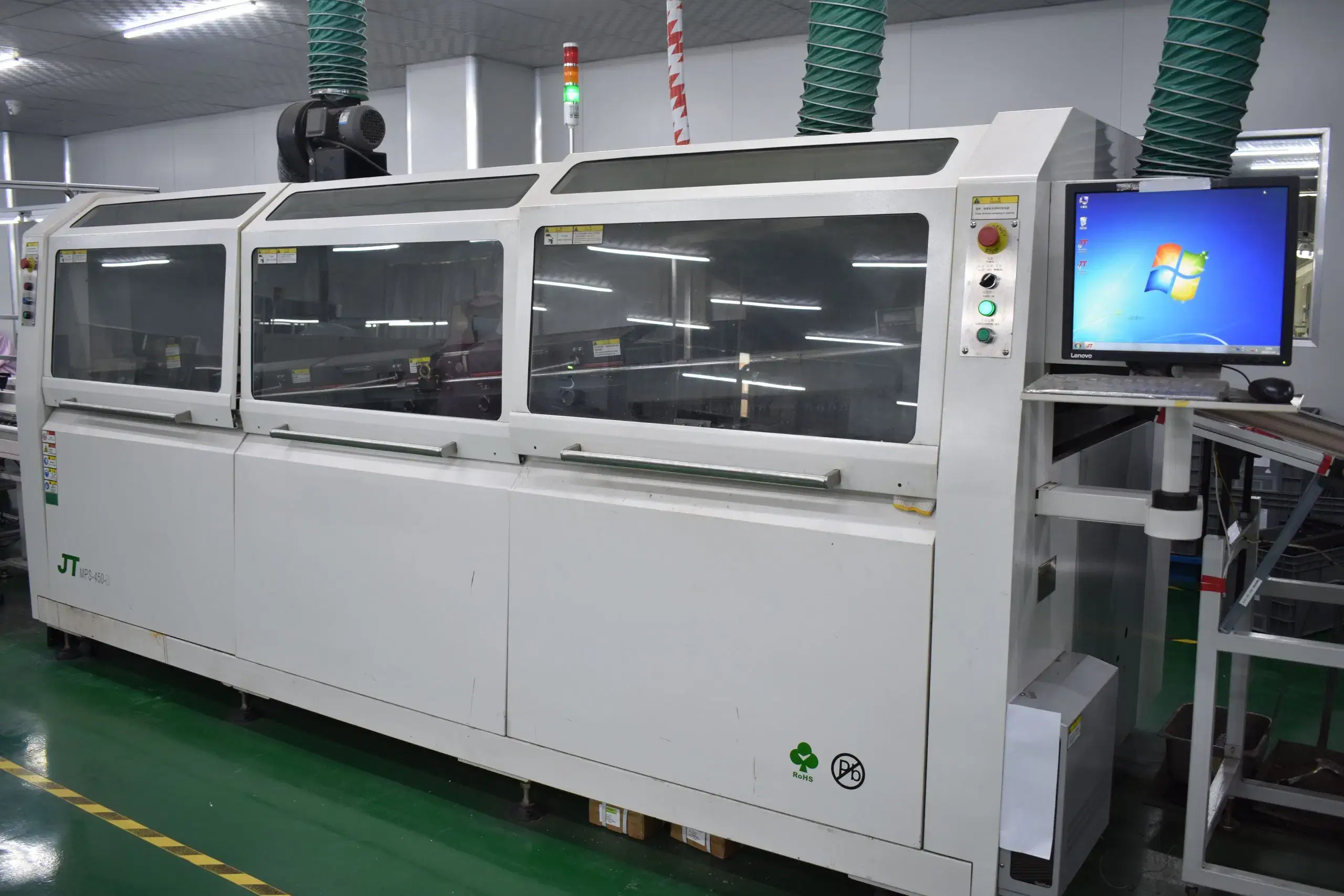
Our PCB Factory Gallery