Upload BOM & Gerber
-
Mobile: +86 13312967631
-
Email: sales@sugaintl.com

Manufacturing Defect Analyzer Testing Services
MDA Testing for Early Manufacturing Defect Control
From CAD and netlist alignment through fixture engineering, production screening, fault localization, corrective action, and documented retest.
7 Defect Categories
Unpowered Structural Screening
Revision-Controlled Test Programs
IPC-A-610J & J-STD-001J Acceptance References
What Is MDA Testing?
MDA Testing for Assembled PCBAs
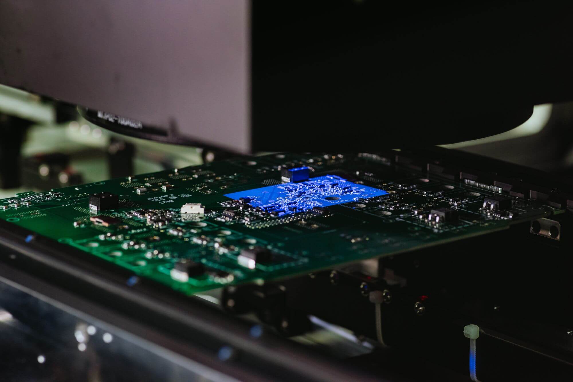
MDA testing of an assembled PCBA is an initial assessment before more rigorous powered electrical testing of the assembly. The MDA process begins without power applied to the entire assembly. MDA confirms continuity, isolation, and selected component signatures through comparisons against programmed limits. MDA is designed to detect opens, shorts, incorrect or missing components, incorrect polarity, and other assembly faults defined in the released test program.
MDA may refer to Manufacturing Defect Analyzer, Manufacturing Defect Analyser, or Manufacturing Defects Analyzer. Each vendor has slightly different terminology for this process; however, the term is generally accepted as an unpowered ICT technique focused on assembly defects. Some test platforms consider MDA a reduced-capability ICT configuration rather than an entirely different architecture. The MDA process is designed specifically for an assembled PCBA and is not intended to test a bare printed circuit board.
MDA Compared with Other Electrical Tests
Electrical testing of a bare PCB confirms continuity and isolation before components are installed. The process of assembling a PCB may alter the expected electrical structure of the completed assembly and typically requires retesting to ensure that its electrical characteristics conform to design requirements. A typical ICT platform adds broader component, analog, digital, and optional powered measurements. FCT powers the PCBA and verifies specified operation under defined loads, interfaces, firmware, and acceptance limits.
Standards Relevant to MDA Testing
While IPC-A-610J and J-STD-001J support assembly-acceptance and post-rework decisions, neither IPC-A-610J nor J-STD-001J defines a universal MDA testing method or a minimum percentage of assembly coverage during the MDA testing process. IPC-9252B addresses the electrical testing of bare printed circuit boards, not assembled-PCBA MDA testing. The electrical coverage of the MDA process is defined by the combination of the test program, revision linkage, limit set documentation, and coverage record that define which electrical tests were performed.
What Defects Can MDA Testing Detect?
The amount of MDA coverage may vary based on the combination of design data, physical access to nodes, programmed limits, circuit topology, fixture contact, and tester capabilities.
| Fault Mode | Electrical Signature | Access Condition | MDA Diagnostic | Next Confirmation Step |
|---|---|---|---|---|
| Open circuit | No continuity on the programmed net | Direct node access or supported indirect method | Failed net, node, connector pin, termination, or trace region | Inspect solder joints, terminations, connectors, and the affected trace region. |
| Short circuit or solder bridge | Low resistance between isolated nets | Access to both programmed networks | Shorted network pair matched to design data | Inspect the mapped network pair for solder bridging, insulation damage, or trace defects. |
| High-resistance or intermittent connection | Resistance above limit or variable across repeated contact | Repeatable contact and defined resistance limit | Board defect versus fixture-contact instability | Repeat under stable loading; inspect solder, cracking, contamination, and termination damage if the failure remains. |
| Missing or incorrectly connected component | Missing signature or network-pattern mismatch | Access to the component network | Signature comparison against BOM, netlist, and limits | Verify placement, seating, connector insertion, and part identity against assembly data. |
| Wrong passive value | R/C/L response outside programmed tolerance | Measurable or compensable circuit path | Failed component network under topology-aware limits | Use isolated component measurement, ICT, or FCT evidence where parallel paths mask the value. |
| Reversed diode or supported polarized component | Forward/reverse junction mismatch or validated orientation signature | Measurable polarity-sensitive path or supported orientation method | Direction or orientation response outside the programmed expectation | Confirm markings, placement direction, and the actual component type. |
| Vectorless IC, BGA, or connector open | Abnormal sensor signature without direct pin probing | Compatible fixture, sensor, geometry, and program | Supported vectorless open-pin diagnostic | Use X-ray, boundary scan, ICT, or targeted trace analysis to confirm package attachment and the affected pin path. |
Component Signature Testing
The test program compares measured signatures with the BOM, netlist, component data, circuit topology, and released test limits. Through this comparison, the tester can reveal discrepancies in the component’s expected electrical characteristics in terms of resistance, capacitance, and inductance values, component presence, diode polarity, and overall network patterns. MDA can identify these types of discrepancies where a measurable component signature exists.
Circuit components may not always be completely isolated. The presence of multiple circuit paths (parallel), circuit protection devices (fuses, surge protectors, etc.), allowable component tolerances, residual charge (on capacitors, etc.), and the overall measurement range can create variations in what appears to be the same component signature. Therefore, MDA must take valid circuit paths into consideration or transfer verification to another method, such as ICT, isolated component testing, programming verification, or FCT.
Vectorless Open-Pin Detection
An MDA system that has a validated vectorless sensing capability can extend the test coverage of circuit integrity, along with passive testing of open pins on selected compatible ICs, BGAs, fine-pitch leads, and SMT connectors, without needing to probe each open pin directly. The amount of test coverage will depend on sensor accessibility, fixture design and fabrication methods, device construction and shape, adjoining circuits, and corresponding correlation data.
Vectorless open-pin test results do not equate to a complete functional evaluation of the board. If a direct probe or valid indirect sensing does not provide repeatable results, the open pin or node will need to be documented as excluded from vectorless testing and reassigned for verification through boundary scan, X-ray inspection, ICT, targeted trace analysis, or FCT.
MDA Test Procedure
- Align design and revision data. All relevant CAD files, board outline information, netlist, bill of materials and manufacturer part numbers, component values, component polarity information, panel map, and revision history records must be consistent with each other to facilitate accurate testing of the physical assembly.
- Generate connectivity and component tests. The engineering staff is responsible for converting the design documentation into expected design-net connections and expected component-signature results. The test program is associated with the target board and BOM revisions.
- Define limits and topology handling. Component tolerances and circuit topology determine the limits of the test program. The engineer compensates for supported parallel paths, and unsuitable measurements are moved to a different method.
- Correlate the program with the fixture. Fixture and program correlation ensures that all programmed nodes are mapped correctly to the fixture probes, tester channels, support positions, and panel units.
- Establish contact repeatability. Target PCBAs and characterized samples, when available, establish land access, board support, stable contact resistance, and repeatable measurements.
- Run production tests and record the result. The fixture and test program will generate measured values, identify failure locations, and provide a pass or fail result.
Design Data Alignment
SUGA develops an MDA strategy using the current CAD data for the board, the netlist, BOM, component data, and PCB revision. The engineer creates checks, limits, probe mappings, fixture requirements, result interpretation, and retest logic for the fixture.
To support MDA development, a single electrical and mechanical definition must exist for the assembly. Variations in test-point, component-value, or panel data can lead to the wrong probe target, expected signature, or limit.
The data that forms the basis of core development includes:
- CAD data for the PCB
- The board outline
- Netlist with reference designators
- BOM/MPN with component values and tolerances
- Polarity and orientation
- Test-point coordinates and probe-side access
- Panelization, tooling, and support
- Revisions to the board, BOM, and assembly
- A known-good or characterized correlation sample, if available
- Existing limits, failure history, and downstream ICT or FCT requirements
MDA Test Limit Setup
CAD and netlist data will assist engineers with automating the initial test program development. However, engineers are responsible for establishing limits, handling circuit topology, applying guarding or compensation where supported, and moving unsuitable measurements to a different defined method.
The released test program should link the board revision, BOM revision, fixture revision, and approved limit set. This prevents a program validated for one revision from being used to test a different physical assembly.
From Fixture Correlation to Production Testing
Fixture correlation uses probe mapping, tester channels, support, and loading to establish expected measurements compared with a characterized sample. Production testing will begin once both contact resistance and measurement repeatability are stable.
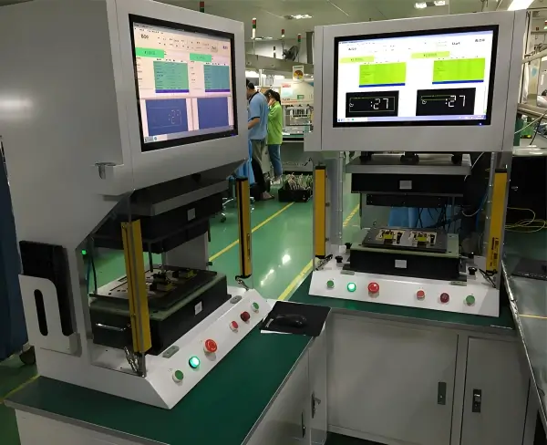
Line integration and board loading are independent decisions. The station may run in an offline or inline configuration; loading may be manual, semi-automated, or automated. Inline systems may coordinate board movement, fixture actuation, and tester result feedback.
Does MDA Testing Require a Fixture?
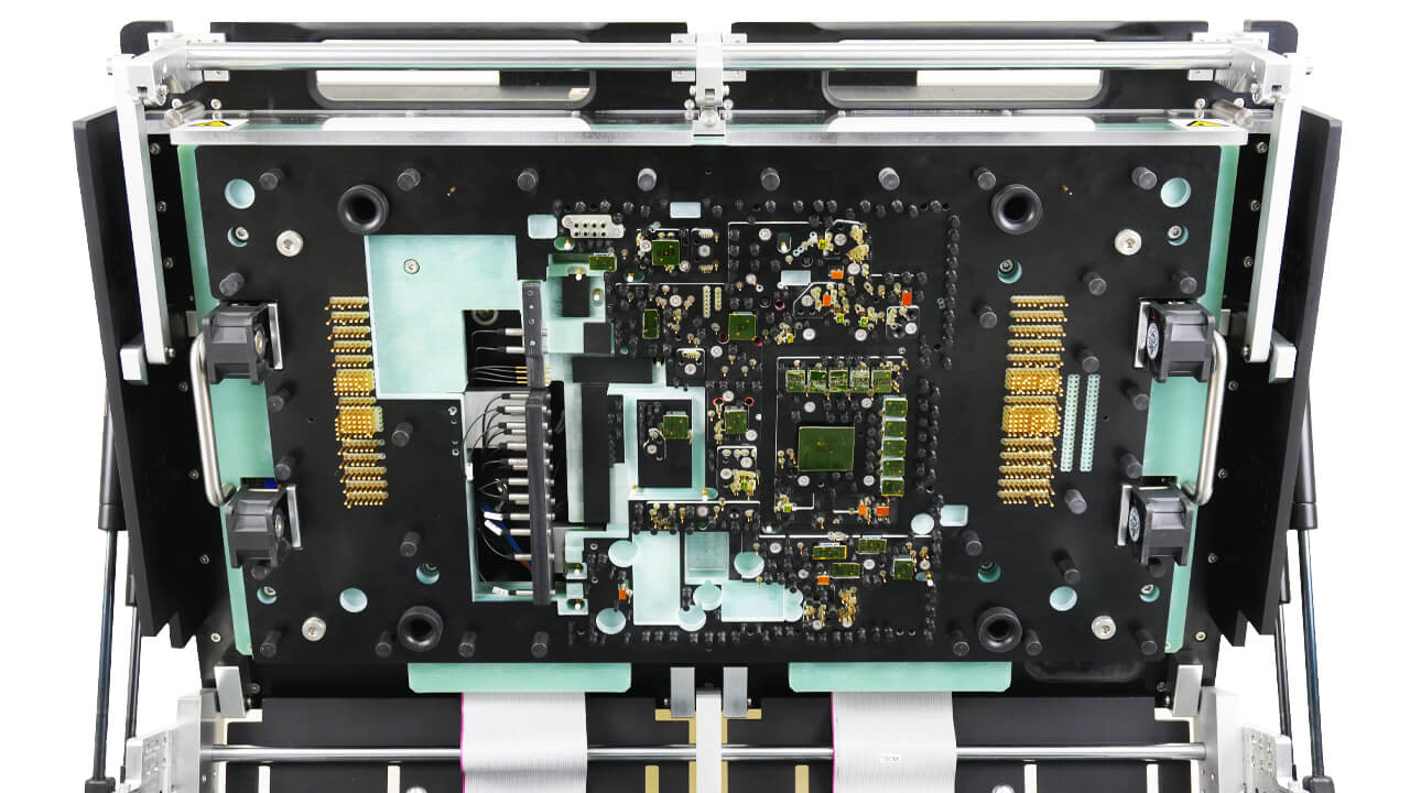
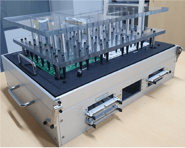
Yes, PCB MDA testing typically requires the use of a board-specific bed-of-nails fixture or a similar fixture. The fixture should provide access to the planned electrical nodes and hold the PCBA flat and stable.
| Fixture Design Factor | Design or Production Input | Test Impact | Fixture Configuration |
|---|---|---|---|
| Board mechanics | Outline, tooling holes, panel rails, support areas, revision | Fixture mismatch or unstable loading | Configure or modify the fixture to match board mechanics |
| Test-land access | Pads, vias, connector contacts, or dedicated test points | Reduced direct coverage | Direct probe, supported indirect method, or alternate test |
| Probe contact geometry | Land size, finish, flatness, clearance, and probe approach | False opens or variable resistance | Probe type, force, support, cleaning, and maintenance |
| Fine-pitch access | Small lands, BGA nets, dense connectors, tall parts, underside congestion, and keep-outs | Probe or fixture-hardware interference | Specialized probes, validated indirect sensing, segmented access, or complementary test |
| Large-board support | Length, mass, stiffness, copper, cut-outs, connectors, and component height | Deflection or unstable multi-probe contact | Support pins, pressure distribution, segmented fields, and vacuum or pneumatic actuation |
| Actuation | Board size, probe count, panel format, loading method, and throughput requirement | Nonuniform contact force | Match actuation to board size, probe count, throughput, and mechanical risk |
| Tester interface | Tester connection, analog resources, probe map, sensor, and software interface | Fixture-program-platform mismatch | Compatible channel and software interface |
Fixture Actuation Options
The bed-of-nails is the mechanism by which the contact structure is defined; vacuum or pneumatic actuation provides controlled pressure to support the probing requirements when the number of probes, the size of the board, or the support requirements exceed those of a simple manual press. Vacuum provides distributed clamping pressure around the sealed fixture area, while the pneumatic mechanism provides controlled force through the press structure. The selected method must provide stable contact without bending or deforming the PCBA, contacting tall components, or otherwise creating pressure-sensitive changes in contact resistance.
Board Access and Mechanical Support
Fine-pitch assemblies do not automatically make good candidates for MDA testing. Small lands, densely packed connectors, BGA-related nets, tall components, underside congestion, and keep-out zones all restrict the ability to perform direct probing. SUGA establishes which nodes can be accessed and subsequently validates either indirect testing or a complementary test for the remaining gaps.
A large PCBA has a different mechanical challenge than a fine-pitch PCBA. The PCBA’s mass, cut-outs, inconsistent component and connector heights, connector loading, copper distribution, and other factors can cause the assembly to bend under the broad probe field. Support pin locations should be under mechanically safe and repeatable areas, not under components or unsupported cut-outs. Correlation should also determine whether failure results change based on the board position or actuation pressure. If the results depend on the board position, the support or alignment may be unstable, and the result may not represent a true assembly defect.
The coverage record lists all direct, indirect, excluded, and complementary checks.
| Coverage Category | Recorded Content |
|---|---|
| Planned networks | Nets and component signatures in the defined test strategy |
| Direct probe coverage | Nodes contacted by fixture probes |
| Indirect or validated vectorless coverage | Pins or signatures measured without direct access to every pin on compatible platforms |
| Programmed component checks | R/C/L, diode direction, presence, and validated polarity-sensitive checks |
| Excluded nodes | Nodes limited by topology, access, or test method |
| Complementary tests | ICT, FCT, boundary scan, AOI, X-ray, flying probe, or other defined methods |
| Revision traceability | Board, BOM, program, fixture, and coverage-record revisions |
MDA coverage should not have a single percentage assigned to it without an explanation. The percentage of nodes directly covered, the percentage of nodes covered through programmed component checks, the percentage of nodes validated through indirect checks, and the percentage of excluded nodes should have separate denominators and should be listed separately in the report.
Fixture Reuse After PCB Changes
- BOM value or tolerance changes: Where there is no change to board mechanics or probe targets, the current fixture can typically remain. The affected limits must be changed, and the measurements must be correlated with known-good samples.
- Test-point or land changes: Changing the location or size of an existing test point or test land will require updates to the probe position or contact method, node mapping, and contact correlation.
- Netlist or polarity changes: Ensure that existing probes are reaching the intended nodes, update the affected tests, and correlate any electrical checks that have changed.
- Mechanical or panel changes: Changes to the board outline, tooling, support points, panel format, or component height may require fixture modification or replacement, followed by renewed mechanical, contact, and electrical correlation.
What Drives MDA Test Cost?
MDA costs separate one-time fixture and program engineering costs from recurring board-test cycles. The main factors affecting MDA test costs are probe count, accessible-node coverage, board support, panel format, tester interface, correlation effort, anticipated fixture reuse, and design revision frequency. Recurring PCBA batches, long downstream FCT, or expensive escaped defects improve the business case for implementing a quick structural screen with MDA. A low-volume lot may still justify MDA testing when fault localization and downstream test time are costly, while a high-volume lot may not benefit from MDA testing if the board changes frequently or does not have adequate direct coverage.
MDA Test Results
An MDA result confirms whether the programmed, accessible continuity and component-signature checks have been completed within the established limits for the current fixture, test program, and board revision.
Connectivity and component-signature results should be compared against the coverage record, measured values, established limits, and the contact condition of the probe tips at the test points. If a result is flagged as a failure, it indicates an electrical mismatch but does not prove that there is a physical defect.
Follow-up inspection or complementary testing will be required to verify whether the cause of the failure is related to solder, component identity or orientation, a damaged trace, a poorly seated connector, inaccessible active circuitry, or a program or contact issue.
An overall MDA pass means that every released check assigned to MDA passed on the recorded PCBA revision. It does not ensure that the firmware operates properly, that the assembly performs correctly under load, or that environmental reliability requirements are met. It also does not cover nodes assigned to another test method.
From Electrical Fault to Physical Cause
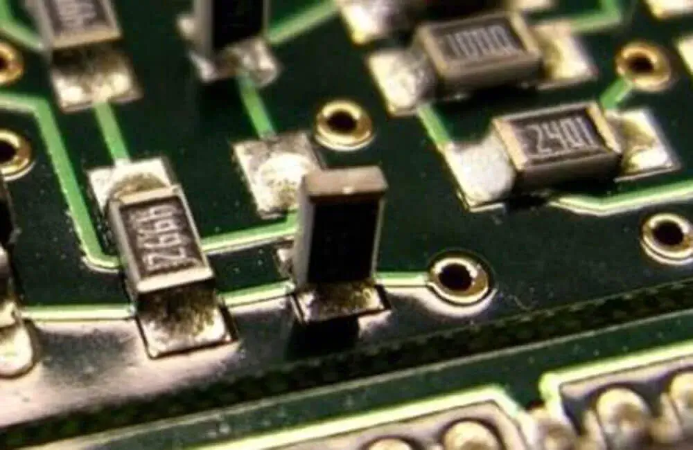
With MDA, the electrical fault can be identified and traced back to a specific net, node, reference designator, connector pin, or suspected area. The search for the physical cause no longer begins without a target.
MDA does not provide the physical root cause of the electrical fault. Confirmation of the root cause is performed using AOI, X-ray inspection, microscopy, mechanical inspection, isolated component measurement, or failure analysis to determine whether the cause is a bridge, cracked joint, damaged trace, wrong part, connector damage, contamination, or another defect.
MDA, ICT or FCT?
The test type chosen depends on what must be proven: whether the structural assembly is intact, whether the electrical behavior at the component level is correct, or whether the product functions when powered.
| Test Type | Primary Coverage | Power State | Access Architecture | Diagnostic Output |
|---|---|---|---|---|
| MDA | Structural manufacturing defects: continuity, isolation, selected component signatures, direction, presence, and validated open-pin checks | Normally unpowered | Board-specific fixture with direct probes and optional validated indirect sensors | Localized manufacturing-defect result |
| ICT | Components, networks, voltages, currents, digital functions, and selected powered parameters | Primarily unpowered, with optional powered measurements on equipped platforms | Higher node and channel demand, guarding, analog/digital resources, and optional powered stimulus | Deeper component and network diagnosis |
| FCT | Specified operation under input, load, firmware, interface, output, and safety conditions | Powered | FCT fixture, supplies, loads, interfaces, instruments, and software | FCT measurements, fault codes, and pass/fail under programmed operating conditions |
When ICT Adds More Diagnostic Depth
Similar to MDA, ICT uses CAD data, netlists, fixtures, and revision-control systems. The key difference when adding ICT to MDA is the addition of diagnostic tools that provide measurement capabilities for active devices, voltages, currents, digital signals, and selected powered parameters.
Select MDA when the primary objective is fast structural screening for accessible manufacturing faults. Select ICT as the primary diagnostic tool when more in-depth component-level diagnosis or a broader range of analog and digital measurements is required. FCT shows how the PCBA operates under powered conditions with an electronic load and programmed firmware.

What FCT Adds
FCT answers the question left by structural screening: whether the assembled PCBA will perform correctly under power, firmware, and load as a complete system instead of simply measuring isolated electrical signatures. Even though a component may measure correctly under isolated conditions, it can fail due to logic behavior, timing, or thermal variation once powered because of its interaction with other components in the circuit.
SUGA can combine MDA, ICT, and FCT into a single test strategy. However, FCT applies only to the programmed operating conditions and acceptance limits.
How Are MDA Failures Diagnosed and Retested?
Diagnosing an MDA failure requires separating a repeatable PCBA failure from false failures caused by probe contact, fixture mechanism issues, program limits, or revision mismatches.
| Failure Source | Diagnostic Signal | Corrective Response |
|---|---|---|
| PCBA manufacturing defect | Repeatable failure after stable contact is established | Localize, physically confirm, repair or disposition, and retest |
| Probe/contact issue | Result changes with cleaning, loading, or contact repeatability | Correct contact condition and repeat correlation |
| Fixture alignment/support issue | Failure follows board position, deflection, clamping, or support | Correct fixture mechanics and repeat correlation |
| Program/limit issue | Design data and measured behavior disagree | Correct program, record revision, and correlate affected tests |
| Revision/data mismatch | Board, BOM, netlist, panel, or test data mismatch | Stop testing until the data set and physical assembly align |
MDA Failure Localization
High, variable, or increasing resistance from successive tests requires the same repeatability and contact-dependency criteria. If cleaning or loading removes the resistance, the cause of the failure is the contact between the probes and test points, not the component itself. The measured values and design data then indicate the failure location—whether a net, node, reference designator, connector, or area—through the relationship between the design data and the measured value from the failed board. After identifying the failure location for the confirmed failure, the known-good or characterized sample may also serve to validate the results. The known-good or characterized sample provides a physical reference for the expected signature of a properly assembled PCB. Therefore, an atypical but accepted measurement will not be interpreted as an issue, and a marginally failing measurement will not be treated as noise.
Retest After Correction
Confirmed defects on a board are either repaired or dispositioned at the solder joint, component, trace, or connector level, followed by retesting with the released program. If there is a problem or fault with either the fixture or the program, corrective action should occur, and correlation must be re-established. The limits established for testing must reflect the target design and must not be widened simply to give a failed board the appearance of a pass.
Traceable MDA Test Records
An MDA report should provide a record of both passes and failures. The report must also include the board identifier, such as the serial number, production lot, position in the production panel, revision level of the board and BOM, revision level of the program and fixture used, coverage revision, test date, and identification of the test station or setup. The list of failures should include identification of the net, node, reference designator, or suspected failure area for each entry, along with the measured value, limit, classification, corrective action, and retest result.
SPC and trend analysis allow differentiation between issues resulting from process drift and those stemming from fixture degradation. Repeated failures at the same reference designator, panel position, connection point, or passive network indicate potential issues with placement, printing, reflow, or board handling. If results change with probe age, use frequency, cleaning interval, board position, or loading pressure, the contact system or fixture may require maintenance.
MDA Testing Applications
PCB MDA testing helps identify accessible structural failures before longer powered tests are performed.

High-Volume PCBA Screening
There is greater value in MDA testing when the same fixture, program, and program revision are used for multiple PCBA lots. A key risk of MDA testing is result drift. When probes are worn, contact resistance can increase throughout the test run and cause some PCBAs to be flagged as failures that appear to result from a process change. Cleaning the probes may clear these false failures.
For each result, the panel position, cleaning interval, and program changes should be documented to prevent false opens from being mistaken for a defect trend. Parallel testing decreases cycle time but increases the number of probes used, which increases the demand for failure identification.
Automotive Lighting Modules
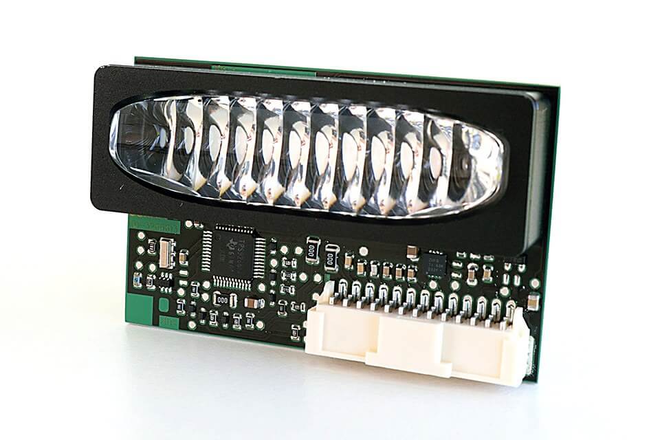
Automotive lighting modules typically contain high-current connectors, protection diodes, current-sense resistors, multiple parallel LED branches, and substantial copper areas used as heat sinks. A single shorted LED branch can pass structural screening. When an LED branch shorts, current redistribution can occur through the other branches. The defect may not become visible until dimming or thermal behavior is checked under power.
MDA can test accessible connector paths, determine whether there are local shorts, and verify diode direction and presence before the circuit is activated. LED regulation, dimming, communication, and performance under load still require FCT.
Industrial I/O Controllers
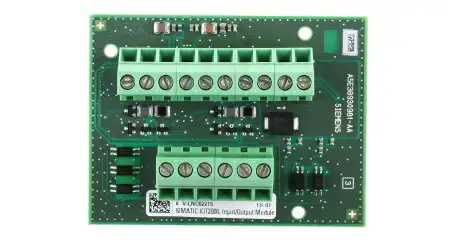
Industrial I/O and PLC circuit boards feature tall terminal blocks and include relays, optocouplers, TVS, filters, and analog circuits. A reversed optocoupler can still provide continuity on its I/O leads even though its signal transfer fails. Simply performing continuity checks will not detect this type of polarity defect.
MDA can test accessible terminal paths, local short circuits, and diode direction before applying power to the product. However, isolation withstand, relay operation, and connected field-load response require ICT, hipot testing, or FCT.
Power Supplies and LED Drivers
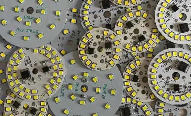
Power supplies and LED drivers contain large bulk capacitors, magnetics, MOSFETs, rectifier components, feedback networks, and high-current connectors. If the previous board has a significant amount of residual charge in its bulk capacitor, this charge can affect the next board’s reading, leading to an apparent intermittent defect when the cause is an incomplete discharge cycle.
MDA can perform structural short, continuity, and diode-direction tests on circuit boards before applying power to the product. Startup, regulation, ripple, and protection require controlled discharge and load testing.
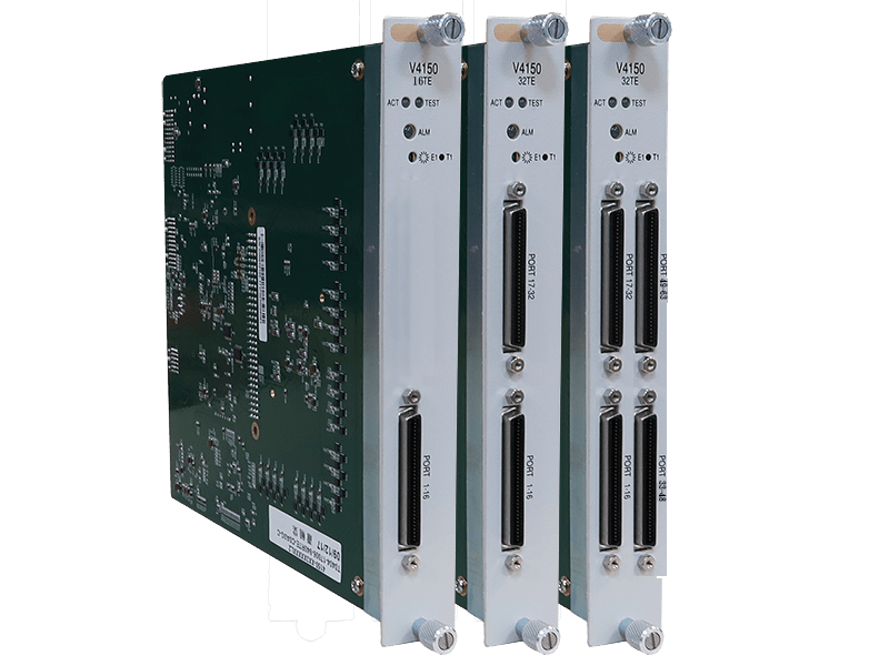
Telecom Interface Boards
Telecom interface boards include high-pin-count connectors, magnetics, protection devices, processors, and complex BGA routing. A reversed differential pair can pass net-level continuity because both traces remain connected, but the polarity reversal will not be evident until a link or signal-integrity test is performed.
MDA can check accessible paths and local shorts on telecom interface boards. However, dense device routing and limited access can make it difficult for MDA to cover these defects. A structural pass will not verify differential impedance or bit-error rate; boundary scan and communication tests cover those paths.
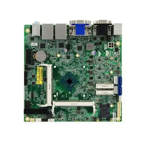
Embedded Appliance Controllers
Embedded appliance controllers typically have a mixture of relays, sensors, connectors, heater or motor interfaces, polarized devices, and low-voltage and high-voltage regions. A heater relay wired to an incorrect contact bank can still pass continuity and presence checks while causing a live-neutral crossover when power is applied to the circuit.
MDA can identify accessible connection, orientation, and passive-network defects before simulating appliance operation. Insulation withstand, relay or motor switching, and control-sequence tests require safety testing and FCT.
Our PCBA Production Lines
















MDA Testing FAQs
MDA can only flag a component as being incorrect if the installed component changes a measurable value, polarity response, presence signature, or network pattern. A same-value substitute, an active component with no differentiating unpowered signature, or a component hidden by parallel paths may pass MDA checks and require AOI, component identification, ICT, programming verification, or FCT.
Most false failures are a result of contamination, probe wear or misalignment, insufficient board support, varying probe contact force, residual charge, unstable limits, or revision-data mismatch. To classify the result as a PCBA defect, the measurement should be repeated under similar controlled loading conditions while comparing the performance of the probe, the board position and panel unit, the cleaning interval, and characterized samples.
Yes, MDA can test assemblies with limited access to test points; however, the coverage record must differentiate between directly probed nodes, validated indirect checks, nodes that are excluded from testing, and the complementary method assigned to each gap. Depending on the specific design of the assembly, compatible vectorless sensing may test selected package or connector opens; however, dense BGAs, high-speed BGA networks, and shielded networks may still require boundary scan, X-ray inspection, ICT, flying probe, or FCT.
MDA testing is usually performed before device programming because MDA testing is designed to identify and correct structural assembly defects that do not require firmware. However, if the next test step requires boundary scan, device configuration, or a product-specific sequence, programming may be done before MDA testing. The released process should define the programming sequence and maintain traceability of the programming status by board serial number or lot.
MDA confirms only the released structural and component-signature checks. Firmware execution, link establishment, communication timing, loaded outputs, safety behavior, and programmed control sequences require FCT evidence, boundary-scan test evidence, or other powered test evidence.