Upload BOM & Gerber
-
Mobile: +86 13312967631
-
Email: sales@sugaintl.com

Free PCB DFM DFA Check Before Manufacturing
Connect PCB Design, Assembly Engineering and Volume Production
Using DFM and DFA reviews to check PCB fabrication data, component placement, soldering access, inspection points, and test conditions is an essential step before any design goes into repeatable PCB fabrication and PCBA assembly.
0.2 mm minimum BGA pitch0.15 mm minimum QFP lead width±30 µm placement accuracy at 3σ
Flying ProbeFixtureImpedanceSolderabilityThermal ShockHole ResistanceMicrosection
01005 packages60,000 CPH placement capacityNitrogen reflow50 × 50 mm to 610 × 508 mm board size
What Is DFM/DFA?
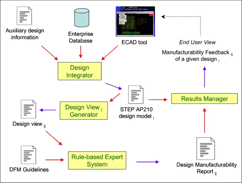
DFM/DFA means checking to see whether a PCB design can be fabricated and assembled repeatably before making final production decisions. DFM examines the board’s fabrication capability. DFA examines component placement, soldering, inspection, access, orientation, and rework procedures. DFMA connects DFM and DFA when a design choice affects the board fabrication process and the assembly process at the same time.
| Discipline | Design object | Outcome | PCB example |
|---|---|---|---|
| DFM | Board fabrication data, material, geometry, and process match | Board can be fabricated repeatedly within process capability | Copper-to-edge clearance; drill allowance; finish suitability |
| DFA | Component placement, soldering, orientation, access, and rework | PCBA can be placed, soldered, inspected, and repaired consistently | BOM/package match; polarity; centroid rotation; inspection access |
| DFMA | Interaction between fabrication and assembly decisions | One design change is checked against both fabrication and assembly impact | Fine-pitch package; pad geometry; finish; paste; thermal connection |
Design for Manufacturing
To design a PCB for consistent production, an engineer must ensure that the stack-up, copper thickness, drill size, and surface finish of the PCB allow it to be produced consistently. DFM gives engineers parameters to evaluate how a PCB will be produced based on the materials and tooling available to the manufacturer and helps them make an informed decision about whether the PCB can be produced consistently.
Design for Assembly
DFA gives engineers parameters to determine whether parts can be placed and soldered on the assembly line without ambiguity and whether they can be inspected and repaired. Engineers also must assess the BOM, reference designators, centroid files, orientation, polarity, and access areas of the assembly.
DFA helps ensure that machines, operators, and inspectors have the same reading of the board, which helps prevent discrepancies caused by different interpretations of the intended assembly.
How DFMA Connects Both Disciplines
DFMA allows engineers to combine the benefits of both DFM and DFA when considering how changing one aspect of a design will affect another aspect of the design. For example, changing a pad width for a fine-pitch part may affect soldering and inspection; thermal reliefs must still be considered when designing a PCB.
DFMA does not erase the two owners. Fabrication still owns board capability. Assembly still owns placement and soldering.
DFM vs. DFA in PCB Engineering
DFMA engineering is needed when a design object, such as a pad, finish, thermal relief, or fixture constraint, can affect both the fabrication capabilities of the manufacturer and the assembly capabilities of the assembler.
| Question | DFM focus | DFA focus | Joint decision |
|---|---|---|---|
| What can fail? | Imaging, etching, drilling, plating, profiling, or finish | Placement, soldering, insertion, inspection, or rework | Package-to-pad match and thermal behavior |
| What changes? | Board geometry, stack-up, material, holes, copper, or finish | Component, land pattern, polarity, orientation, or access | Pad, paste, finish, thermal connection, or panel access |
| Who decides? | PCB fabrication engineering | Assembly and process engineering | Design, fabrication, and assembly engineering together |
| What proves it? | Fabrication data matches a demonstrated process | Assembly data supports repeatable placement and soldering | Both processes accept the same design condition |
Which Risks Belong to DFM?
DFM is concerned with the PCB fabrication process. PCB DFM risk begins with the bare PCB, including geometry, material selection, stack-up, copper distribution, hole design, surface finish, and edge profile. If the PCB manufacturer cannot define and repeat the construction based on the released data, the risk belongs to DFM.
A good example is copper-to-edge geometry. A component may be correct, but the routing path or exposed-copper condition can still make fabrication difficult. Drill-to-lead allowance is similar; the finished hole must provide clearance for plating and insertion before assembly can depend on it.

Which Risks Belong to DFA?
DFA risk begins with placing components on the PCB and verifying that they survive soldering, inspection, and service. The main concerns for DFA include package consistency, polarity, switch state, connector direction, solder access, and rework space.
There are multiple DFA checks for the same component. The land pattern must match the package. The paste must support the solder joint. The rotation in the placement data must match the package drawing and visible markings. The inspector must have adequate visibility to verify the result.
When Should DFM and DFA Work Together?
When DFM and DFA impacts share a common decision, it is necessary to jointly review the impact on both processes. For example, while a particular finish might be acceptable for many pads, a fine-pitch assembly may show that it should be reviewed for a specific package.
Thermal connections can help improve electrical performance, but they can also pull heat away from the joint during soldering. A panel format can make fabrication easier, but it may limit fixture access during assembly.
The same design decision can create different consequences for each process. The question is whether fabrication and assembly can both accept the same condition.

PCB DFM Guidelines
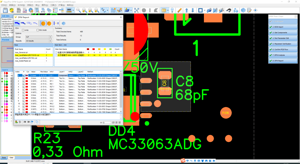
PCB DFM guidelines should be organized around complete and consistent fabrication data, then geometry, finish, drill-to-lead allowance, thermal connection design, package-to-pad compatibility, and process-dependent edge clearance. The table below identifies the numeric trigger and level of severity for each guideline; the following sections explain how each trigger affects the real build.
| Rule | Level | Impact | Use |
|---|---|---|---|
| Components smaller than 0402 or pitch below 0.5 mm | High | Surface finish and pad flatness need review | Check package geometry, soldering method, and storage; review package and process together, not in isolation |
| QFP below 0.5 mm pitch or BGA below 1.27 mm pitch | High | Finish flatness can reduce soldering margin | Use as a finish review trigger tied to fine-pitch geometry, not a universal rule for every finish |
| BGA pad below 10 mil / 0.25 mm | High | Small pads make finish selection more critical | Treat pad size, finish, soldering, stencil, and inspection as one decision |
| Gerber parameters agree across material, Tg, thickness, finish, stack-up, mask, silkscreen, copper, and impedance | High | Conflicting data can define different boards | Confirm one controlled board condition and resolve conflicts before release |
| Thermal relief matches component, pad purpose, copper area, current, and soldering process | High | Poor thermal choice can affect soldering or heat transfer | Judge the electrical need and the soldering behavior together, not the electrical need alone |
| Package geometry matches solder-paste design | High | Land-pattern or paste-volume mismatch can create solder defects | Check package, pad, mask, stencil, and assembly process as a single condition |
| Drill and finished hole match lead and plating requirements | High | Wrong allowance can cause insertion or solder-fill problems | Check the final plated size, not only the drill callout, against the soldering process |
| Copper-to-edge, slot, and profiling conditions match the selected process | High | Edge damage or exposed copper risk increases | Tie clearance to the actual process and confirm against the selected profiling method before release |
| Mask, silkscreen, paste mask, via tenting, and panel choices are readable for production | Review | Markings, mask assumptions, or panel handling can drift | Treat these as manufacturing data controls; confirm the operator can read and build the board |
When standards are part of the project, use them as engineering language: IPC-2221C for generic board design, IPC-7351B for land patterns, IPC-4552B for ENIG requirements, IPC-A-600M for bare board acceptability, IPC-6012F or IPC-6013E for board performance, IPC-A-610J for assembly acceptability, J-STD-001J for soldering requirements, and IPC-7711/21D when rework or repair requirements are defined. Apply them when specified, where required, or per the customer-defined acceptance class.
Board Fabrication Rules
Fabrication rules should be followed in a hierarchy, with the order more important than any single fabrication rule. First, every design file must represent the same circuit board. If a Gerber file calls for one finish while the drawing calls for another finish, this is not a small typo. It leaves fabrication without a confirmed condition to build to.
Only after data consistency is confirmed does physical geometry become useful for review. A routing profile, V-cut, or plated slot can change the edge condition enough that a rule which appears safe on paper may fail once the selected process is used.
Surface Finish Decisions
The rows labeled "Finish" in this table are not restrictions against employing any of the different types of finishes; however, they do provide enough information to allow for a collective examination of package pitch, pad size, soldering method, storage condition, stencil design, and supplier process capability; e.g., a finish that is acceptable on a 0.65 mm pitch package may provide virtually no margin of safety on either a 0402-sized component or a fine-pitch BGA.
One failure mode that occurs with some degree of regularity is when a project specifies a finish early on, based on cost and shelf life of most of the components, and then later adds fine-pitch BGAs during the design phase of a project. Without re-evaluation of the finish specification for the new part, fabricating the board may pass through the DFM process with no issue, but the assembled board may display marginal solder joints under the BGA balls. This problem typically cannot be detected by an AOI system and typically requires either X-ray inspection or a field return to establish the issue.

Fine-Pitch Assembly Constraints
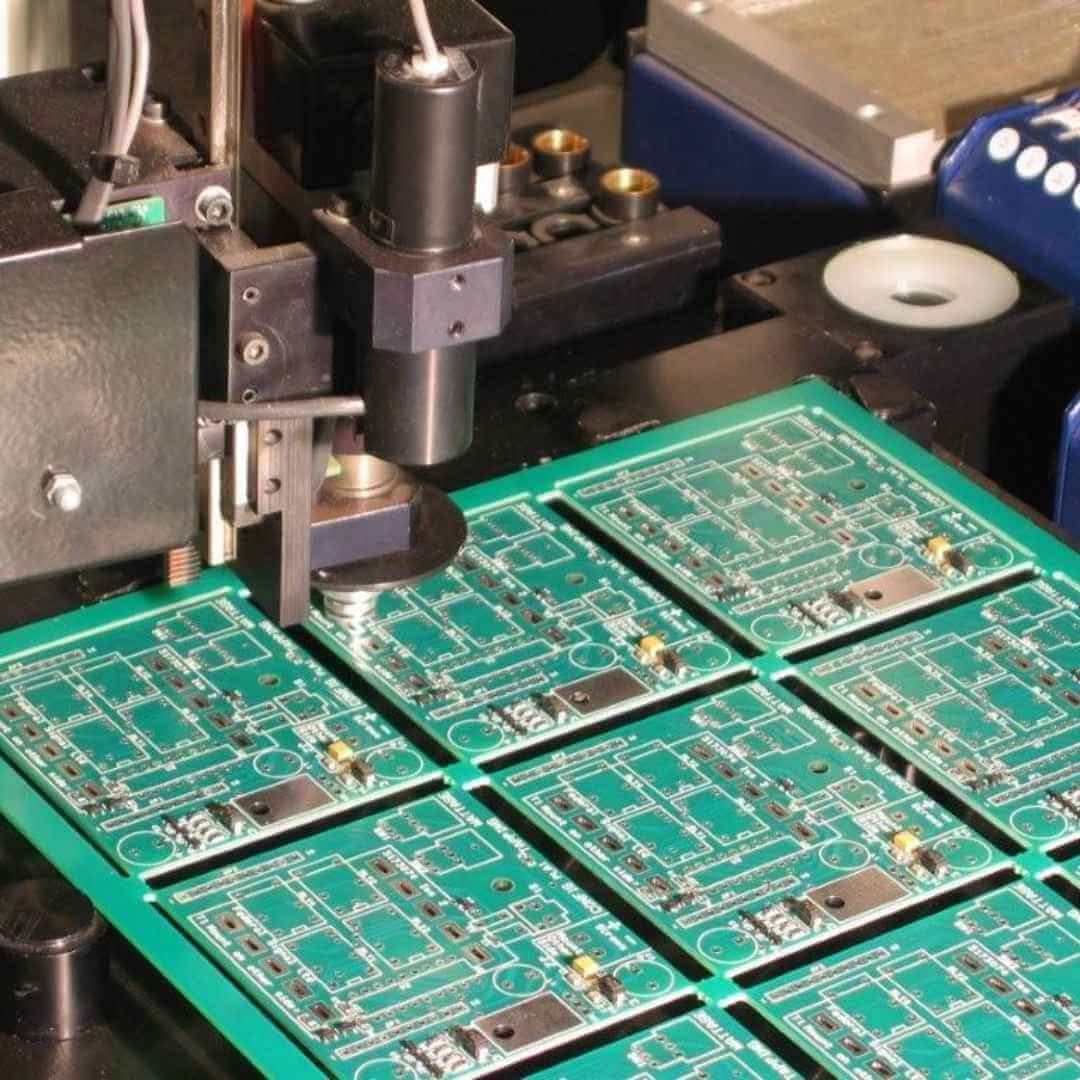
The use of fine-pitch and BGA assembly creates very little room for making assumptions. Factors such as pad flatness, stencil selection, paste volume, reflow behavior, and inspection method must all be considered together more closely on fine-pitch and BGA assemblies than they will on other types of PCB assemblies.
While a BGA assembly conceals most joints from view when visual inspection is performed, a dense QFP will yield visibility of the joint; however, the paste deposit and lead geometry can provide limited tolerance for mismatch.
Therefore, it is important to maintain two separate sets of figures on this item; i.e., the finish-review triggers for the 1.27 mm pitch BGA and the 10 mil / 0.25 mm pad sizes; and the 0.2 mm minimum BGA pitch and the 0.15 mm minimum QFP lead width used to identify what the placement line itself can handle. Therefore, even though a board is comfortably within the limits of the placement capability for a given line, that same board can still trigger a finish review because the two separate figures provide answers to two different questions, i.e., equipment reach vs. solder-joint risk.

Board Markings Affect Production Consistency
The information contained in the mask, silkscreen, paste-mask data, via tenting, and panel choices may appear to be unimportant and only appear to provide cosmetic information to the board until production begins reading and reproducing these items on a repeated basis. The information provided to operators shows them where to locate various openings, how silkscreen markings should be read, and how the board should be handled and separated throughout production.
If a silkscreen marking cannot be located after component placement is completed, it serves no purpose to the manufacturer. A panel design that allows for manufacturing but does not allow fixture access will create a later conflict during assembly. All of these items should be treated as manufacturing controls; the cosmetic aspects are secondary.
PCB DFM/DFA Checklist for Assembly
A PCB DFM checklist for assembly serves to demonstrate that the released data provides information to carry out placement, soldering, inspection, testing, and rework. Confirm BOM-to-designator consistency, package-to-pad compatibility, placement coordinates and orientation, polarity and pin-one identification, solder access, through-hole allowance, inspection access, and rework clearance.
| Check item | Proof | Risk | Level |
|---|---|---|---|
| Silkscreen includes reference designators with correct orientation | Assembly marks are clear and consistent across board, drawing, and CPL | Ambiguous or reversed placement | High |
| Placement data includes X/Y coordinates, rotation, and orientation | Machine placement data is unambiguous and matches package and board view | Wrong placement from correct machine execution | High |
| BOM part number, quantity, type, value, and references agree | Part identity is controlled across one released BOM version | Wrong part, wrong value, or wrong quantity | High |
| Component package matches solder-paste design | Paste volume matches land pattern and process | Bridging, opens, tombstoning, or rework risk | High |
| Through-hole lead and finished hole match the soldering process | Lead insertion and solder-fill clearance are confirmed against the selected soldering process | Lead fit or barrel-fill risk | High |
| Pin 1 or orientation is visible on asymmetrical connectors and sockets | Installation direction can be verified after placement | Reversed installation | High |
| Switch ON position or pin positions are marked | Assembly state is visible before test and matches FCT expectation | Wrong switch state | High |
| Soldering, inspection, test, disassembly, and rework access are available | Assembly can be verified and serviced as part of the design, not an afterthought | Placeable but unserviceable assembly | Engineering priority |

BOM Data Must Match Placement Files
Assembly begins with identity, not geometry. If one file calls R14 a value that the BOM assigns to R41, production has to stop, because the machine cannot resolve the naming conflict on its own. The machine will place whatever the file says, correctly or incorrectly, with the same level of confidence.
The requirement for released-version discipline is greater than for any individual field check. If the BOM is revised one day after the placement file is released, or if a last-minute substitution is done by email instead of through the controlled BOM, it creates the same R14/R41 issue even though the files may look correct independently. The proof column exists to show one released version, not one correct-looking file.
Package Match Controls Soldering Risk
The controls for component soldering risk depend on the soldering method and the connection type. For SMT, the component package, land pattern, mask opening, stencil, paste deposit method, and reflow method must match as one condition. A minor mismatch can lead to bridging, insufficient solder, tombstoning, or repeated rework.
Through-hole parts must be checked separately. The lead diameter, finished-hole size, plating allowance, and soldering method must match the through-hole assembly process. The assembly process sees the final board geometry, not the intended geometry.
Placement Markings Must Be Clear
Placement markings must be clear on the circuit board. Pin-one marks, diode polarity, connector orientation, socket orientation, switch state, and rotation angles must not be open to interpretation. The machine program, operator, and inspector must all have the same answer when looking at the same board.
For asymmetrical connectors and switches, ambiguity is costly. Production may build a product that functions improperly even though the placement is perfectly repeatable. During the assembly stage, a good design for manufacturability check should determine whether the intended orientation can be confirmed after nearby components, coating, enclosure clearance, or fixture access are considered.
Miniature Components Require Named Controls
Due to the size of 01005 parts and the fine pitch of BGA and QFP packages, there must be specific controls in the production process. At this size, paste, placement, reflow, inspection, and rework are not background assumptions; they are specific decisions that must be identified in the process plan.
This becomes especially important when small parts are inspected. AOI can usually verify the placement of a 0201 or larger part, but an 01005 part typically requires a special optical setting or dedicated inspection recipe. Copying the inspection recipe from a larger-package project can produce inaccurate results for an 01005 part.
Access Determines Verification Coverage
Even though a board can be placed, it may be difficult to inspect, fixture, test, disassemble, or repair. Component height, keep-out zones, connector direction, test-point access, and rework clearance all affect the ability to verify a unit after placement.
DFA typically uncovers risks that are overlooked by a pure fabrication review. If a probe cannot reach the point, the optical system cannot see the joint, or a shield prevents rework access, the design has caused a production issue that cannot be flagged during the fabrication check.

How the DFM Review Process Works
The DFM review process starts with the design-data check, issue classification, engineering feedback, and the production decision.
Design Data Check
The design data check starts with reviewing the design files that define the assembly and board. The files include fabrication data, BOM, assembly placement data, drawings, stack-up, finish requirements, constraints, and assembly notes.
DFM software and CAM rule checks can highlight geometry conflicts, missing layers, spacing concerns, and data inconsistencies. Engineers still need to verify package compatibility, review finish selection, and determine whether the identified conditions change production risk. A check shows only pass or fail, while a DFM review connects the flagged issue to the processes required to build the board.
Issue Classification
Issue classification assigns production meaning to every finding. The same decision should not be made for a missing drill file, ambiguous polarity mark, finish mismatch, or blocked fixture access.
Severity classification represents what would happen during production. Some findings can block release because the board definition is unclear. Other findings require engineering review before they can be accepted.
Engineering Feedback
Engineering feedback should identify the issue, rule, consequence, and practical correction path. If the comment is only a warning, the design team will be uncertain of the action to take. A useful comment tells them what process is at risk and what decision could resolve the risk.
For example, a package-to-paste mismatch should identify the component, pad, stencil, paste condition, and potential assembly consequence. A finish issue should connect package geometry with soldering and inspection processes; it is not enough to simply indicate the preferred finish. Engineering feedback could lead to a design change, a corrected drawing, a revised placement file, or an accepted exception, but the next action must be specific.
Closure Decision
The decision allows the company to proceed with release and production once blocking items have been resolved and remaining conditions are understood. Proof may include corrected design files, released drawings, confirmed process settings, inspection access, or an accepted exception. If proof is still unclear, the issue remains open.
PCB DFM Issues That Stop Production
Some of the highest-risk DFM issues for PCB production are often the least complex. Examples include lack of fabrication data, conflicting parameters, unsuitable finish for fine-pitch geometry, package-to-pad mismatch, ambiguous orientation, insufficient edge clearance, wrong hole-to-lead allowance, blocked access, and unclosed exceptions.
| Issue | Team | Severity | Impact | Proof |
|---|---|---|---|---|
| Missing Gerber, drill, or stack-up data | Fabrication | Blocking when the board is not fully defined | Fabrication cannot define the controlled board | Corrected fabrication package and confirmed stack-up, material, and finish |
| Material, Tg, thickness, copper, finish, impedance, mask, or silkscreen conflicts | Fabrication | Blocking when documents define different boards | Wrong construction, finish, or controlled parameter | One released data set with resolved parameter conflicts |
| Fine-pitch QFP/BGA or small BGA pad finish mismatch | Fabrication + assembly | High when pad flatness affects soldering margin | Solder joint, coplanarity, or inspection risk | Finish matched to package geometry and process conditions |
| Package-to-pad or package-to-paste mismatch | Assembly | High when land pattern or paste volume does not match | Bridging, insufficient solder, tombstoning, or rework risk | Package, land pattern, mask, stencil, and paste confirmed |
| Thermal relief mismatch | Fabrication + assembly | High when soldering or heat transfer is compromised | Poor solder fill, heat sinking, or thermal performance risk | Thermal connection confirmed against pad purpose and copper area |
| Finished-hole allowance mismatch | Fabrication + assembly | High when lead insertion or solder fill is uncertain | Lead clearance, barrel fill, or hand-solder risk | Lead size, finished hole, plating, and soldering method confirmed |
| Edge, slot, or profiling risk unresolved | Fabrication | Blocking/high when exposed copper or edge damage risk remains | Edge damage, depaneling risk, exposed copper, or short risk | Edge clearance and profiling process confirmed |
| Orientation, polarity, pin-one, or switch state is ambiguous | Assembly | Blocking when placement cannot be verified | Reversed placement, wrong switch state, or functional failure | Silkscreen, assembly drawing, CPL, or work instruction corrected |
| Inspection, fixture, test, or rework access is blocked | Assembly + test | High when the build cannot be verified or repaired | Escaped defects, fixture difficulty, or rework loss | Access plan, test points, fixture plan, or rework method confirmed |
| Accepted exception lacks responsibility or proof | Engineering | Blocking when residual risk is undocumented | Repeat-build risk | Responsibility, accepted condition, and production record documented |

Data Conflicts Can Stop Fabrication
Data on how to construct a board is not complete when required information associated with that board is missing, nor can it be determined with certainty from conflicting documents, such as two documents with contradictory information. For instance, if a stack-up is revised to account for impedance but the drawing still indicates the old layer count, the manufacturer will not know which one to use.
By and large, most of the conflicts stem from which document was last modified and which was not updated — a revision made to a stack-up after the layer count changed is a typical real-world conflict.
Production must have one data set to produce the board, with corresponding information for material, stack-up, surface finish, dimensions, and drawing intent across all files production will actually use.
Geometry Choices Can Create Assembly Failure
Geometry and finish can create issues between fabrication and assembly. The geometry for fine-pitch QFP/BGA, small BGA pads, mismatch of package-to-paste, and thermal reliefs all look like design details for the board design until soldering is performed.
The flatness of pads can reduce soldering margin. Paste volume can change the shape of the joint, and thermal connection can either pull heat away from the joint or fail to carry the current path that is expected as part of the design.
These represent advanced DFM checks that can be performed on PCB designs. Unlike more simple items, the issue will more likely be apparent through process interaction than through any one single document that contains an error.
Ambiguous Placement Can Block Assembly
There are boards that can be physically made, but are not recommended for release. Ambiguous pin-one markings, connector orientation, polarity, switch state, or rotation can lead to repeatable wrong placement.
Defects may not be visible after placement. Blocked inspection, fixture setup, testing, or rework access can hide defects after placement and result in production problems.
These are DFA issues with production consequences. A machine may place a component according to the design file and still make an incorrect placement. An operator may solder a connector correctly but leave the inspector unable to confirm orientation.
Severity Depends on Proof
The severity of the finding is resolved by proof, not by simply naming a rule. Corrected files, released drawings, confirmed process settings, inspection access, test plans, or documented exceptions can close a finding. An unresolved comment cannot close the same finding.
DFMA from Prototype to Volume Production
Through prototyping, manufacturing and assembly assumptions are identified; through the new product introduction stage, manufacturing and assembly options are converted into confirmed manufacturing and design decisions. Volume production depends on repeatable placement, soldering, inspection, testing, and documented exceptions.
| Capability | Use | Limit |
|---|---|---|
| 01005 package support | Miniature SMT process planning | Link to paste, placement, reflow, inspection, and rework controls |
| 0.2 mm minimum BGA pitch | Fine-pitch placement planning | Separate from the 1.27 mm BGA finish review trigger |
| 0.15 mm minimum QFP lead width | Fine-lead placement planning | Pair with land pattern, finish, paste, and inspection choices |
| ±30 µm placement accuracy at 3σ | Placement precision planning | Tie to actual placement setup and inspection results |
| 60,000 CPH placement capacity | Throughput planning | Use with line setup, BOM mix, and inspection plan |
| Flying Probe, Fixture, Impedance, Solderability, Thermal Shock, Hole Resistance, Microsection testing | Inspection and testing planning | Select according to project risk and acceptance requirements |
| Nitrogen reflow capability | Reflow process planning | Apply when the soldering process justifies it |
| Board size 50 × 50 mm to 610 × 508 mm | PCB size planning | Confirm panel constraints before build |
What Prototype Testing Reveals
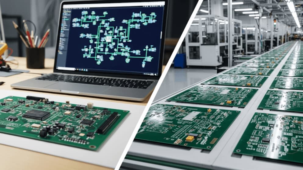
The initial assembly prototype of the PCB validates whether the design assumptions hold true when put into practice during fabrication, placement, soldering, inspection, and test access. It is possible that although a prototype confirms the concept, there may be problems with the PCB finish, pads, orientation, or access to the PCB that need to be corrected before continuing with the next production run.
The information generated is specific to issues that were found. For example, DFM/DFA comments, inspection access notes, or test constraints show the team exactly what needs to be changed before production begins. Conversely, vague approval from a prototype does not provide a means of repeating volume production.
NPI Converts Findings into Released Process Settings
The NPI process provides the basis for how to proceed after the prototype has been made. NPI identifies the change, replacement, or correction of the findings received from prototype testing.
The first article production results, AOI or X-ray records where applicable, test feedback, and observations during production show the team whether the DFM/DFA issues identified in the prototyping stage appear in the actual production of the first article.
The team is now in the position to determine how the PCB can be assembled repeatedly, and what settings, filenames, inspection criteria, substitutions, or exceptions should be established for each production run.
Volume Production Depends on Repeatable Data
Sustained data for volume production requires stable BOM/CPL data, stable process settings, up-to-date inspection plans, test access, and documented exceptions. DFM for PCB assembly does not stop once the prototype works; it continues until the same design and process parameters can be reproduced without rediscovering the same issue.
Inspection and Testing Verify Actual Production Results
Repeat-build stability and inspection test results are two different sources of information. DFM/DFA is a method to confirm that design and manufacturing parameters are controlled before they are released. The data from AOI, X-ray, and functional testing show the actual product of a specific build. When a test escape or first-article defect occurs, it should be documented back to the DFM/DFA record, not merely logged as a production event. It is more important to establish a link to the DFM/DFA record than to create a line between two separate events.
PCB DFM/DFA Application
DFM/DFA uses the same methodology for all electronic products. However, the dominant risk changes with RF layout, power and thermal paths, mechanical stress, coating, traceability, cleanliness, test access, and production history.
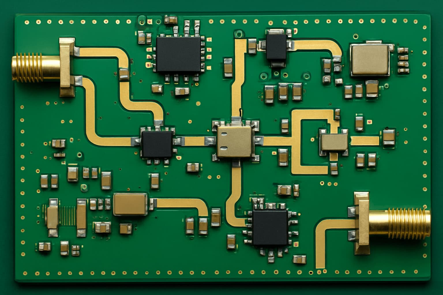
Wireless Boards Require RF-Aware Review
Consumer electronics PCBs and PCBAs typically include low-power operation, compact placement, wireless modules, audio or noise-sensitive areas, charging contact locations, and enclosure clearance. Key checks include component density, finish suitability, antenna and noise keep-out zones, charging interface placement, connector direction, enclosure clearance, and test access.
IoT devices add another layer. Wireless module size, antenna keep-out distance, low-power states, miniature passive components, charging areas, programming header footprints, and serial identity markings all influence the assembly process. Although a PCB may meet the general requirements for placement, it may not meet the product's functional requirements unless antenna clearance and access to measure sleep current are confirmed.
The repeated issue is not where the keep-out zone is located, but who will be responsible for verifying it. A layout tool can determine that no copper is in the keep-out zone, but it cannot determine whether the keep-out zone still matches the most recent reference design from the antenna manufacturer.
Substituting one part with another at a late stage in a project may reduce the actual clearance if nobody redraws what should be kept clear. The only time this situation will become clear is once the keep-out area has been compared against the final bill of materials and not just against the initial design layout.
An additional example is the charging connector. Spring-loaded pogo pins and USB-C receptacles require the electrical connector to fit flush against the mechanical stack-up within an enclosure. If the board thickness or connector-height tolerances pass manufacturing DFM in isolation, the connector may still be recessed or out of position when the enclosure is closed. A bare-board inspection will not detect this issue because it can only appear after the product has been fully assembled.
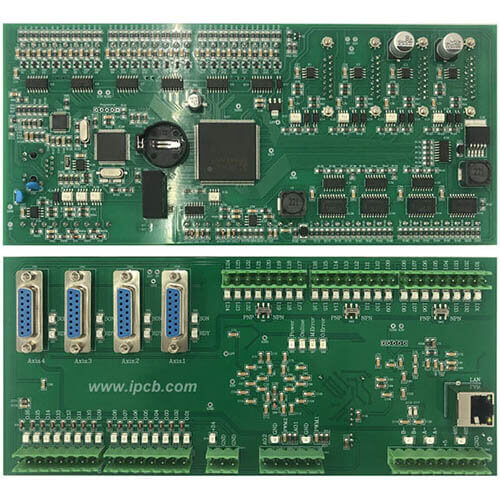
Industrial Boards Require Stress-Aware Review
Industrial automation and control PCBs and PCBAs can include PLC I/Os, sensor modules, motor drivers, interface boards, EMI-exposed areas, connector supports, coating keep-out areas, and operating temperature extremes. These require examination for connector strain support, vibration exposure potential, EMI-sensitive routing areas, high-current paths, conformal coating keep-outs, mounting hole locations, and functional test access.
As for energy and power control PCBs, copper and heat become the predominant items. Copper weight, current path, heat spreading, creepage and clearance values, connector rating, mechanical support, through-hole clearance, conformal coating keep-outs, and load test access will dominate DFM/DFA decisions with those PCBs.
A common connector failure is a connector that passes solder inspection but provides no mechanical support for the strain caused by cable or vibration load on the connector.
If a through-hole connector is fully barrel filled but cracks at the joint months later, then the original design may have relied on the solder joint for retention instead of providing a keep-out for fasteners or strain relief boots. The DFM/DFA record must identify which connectors have mechanical loads and the retention method confirmed for each, not merely that the pads have been soldered correctly.
A second pattern typically occurs in conformal coating processes. A keep-out applied on paper around a connector or test pad may become bridged during production due to the dispensing method being less precise than suggested by the original drawing. The DFM/DFA review must ensure the coating process results in consistent repeatability relative to the keep-out zone, as well as the dimensions specified in the drawing.

High-Reliability Boards Require Stronger Records
When considering high-reliability applications, manufacturers will probably require additional documentation. Medical electronic assemblies must provide means to identify the materials used, cleanliness handling, MSL control, inspection, rework limits, and release once completed.
Automotive electronic assemblies will have higher requirements for vibration, thermal cycling, connector support, polarity, solder-joint inspection, and, if applicable, X-ray/AOI/FCT inspection as well as process documentation.
Telecommunications and communication equipment assemblies will depend more heavily on impedance, RF or communication paths, shielding, connector location, optical and electrical interfaces, thermal path, and test access. When dealing with high-reliability electronics, it is important to provide approved substitutions, traceability, rework limits, environmental exposure limits, and long-term production records. As a result, DFM/DFA should make the records more specific, not inflate the claim.
The most common reason for gaps in traceability on high-reliability boards is that traceability records, both material and process, are kept at too broad a granularity.
In other words, a material and process record that only provides the lot number of the bare board does not suffice for field returns of medical or automotive boards. When performing this kind of investigation, it is important to establish traceability back to the assembly's specific placement run, reflow profile, and inspection results. This only occurs when you confirm what acceptance class granularity your traceability requires before production begins, rather than developing a traceability system after the first field return.
A related pattern with automotive boards is related to solder joints. Solder joints that appear satisfactory during X-ray and AOI inspection of the first article may later fail after several thermal cycles if the joint geometry was optimized for inspection visibility rather than fatigue life. If vibration or thermal cycling are identified as requirements for a product, the DFM/DFA record for the solder joint should reflect that joint's review against those specific requirements rather than just against solderability and inspectability.
Frequently Asked Questions
DFM addresses the possible risks associated with fabrication, including materials, board geometry, stack-up, drilling, copper, finishes, and the capability of the manufacturer to fabricate to strict tolerances. DFA addresses the possible risks associated with assembly, including placement of components, soldering, orientation of parts, access for inspection, and rework. DFMA coordinates both when design choices affect methods for fabricating and assembling the product.
The standard PCB DFM and DFA input files are Gerber, drill files, BOM, CPL/centroid data, stack-up, finish requirements, assembly drawings, and any test notes. These files provide a basis for engineering to determine whether the way in which a PCB will be fabricated and assembled corresponds with the design intent. The end goal of a DFM and DFA review is to create a single board definition across these input files.
No. DFM and DFA reviews determine whether the fabrication and assembly data have been released and whether those data can be produced and placed consistently. Signal integrity, EMC, and thermal simulation are all conducted as separate electrical design reviews and should be completed before conducting a DFM and DFA review. A PCB that passes through the DFM and DFA review process can still fail an electrical design requirement for which it was never evaluated.
Surface finish has an impact on the flatness of the pads used for mounting QFP/BGA devices, their solderability, storage conditions, and the amount of margin that can be tolerated within the assembly when using fine pitch. The choice of surface finish used on QFP/BGA and small-pad designs often needs to be considered in conjunction with the geometry of the package and the soldering method that will be used. The appropriate choice of surface finish will generally depend on the specific design and the process that will be used for that design.
Examples of blocking findings in DFM reviews include missing fabrication data, conflicting finish or stack-up requirements, BOM/CPL mismatches, an unsuitable surface finish, mismatched holes and leads, ambiguous polarity, or blocked access for inspection and testing. Blocking findings in DFM reviews remain open until confirmed data are provided, engineering verifies compliance with the design, or an exception has been documented.
Yes. Prototype reviews provide a better understanding of the assumptions made during the development of the design. The transition of the findings from prototype review into the processes used to manufacture the product in volume production will depend on stable files, DFM/DFA settings, inspection plans, and exception records. This process continues to be repeated as the project grows in complexity: the findings from prototype reviews provide the basis for the manufacturing process settings that will be used in volume production.
No. The purpose of the DFM review is to check if the design is complete and correct regarding fabrication and assembly. AOI, X-ray, ICT, flying probe, and functional testing are used to check actual results from the product in relation to its intended function after or during production. Both DFM/DFA review and production test processes need to be performed, as each process answers different questions regarding product quality.