Upload BOM & Gerber
-
Mobile: +86 13312967631
-
Email: sales@sugaintl.com

How Does Flying Probe Testing Work?
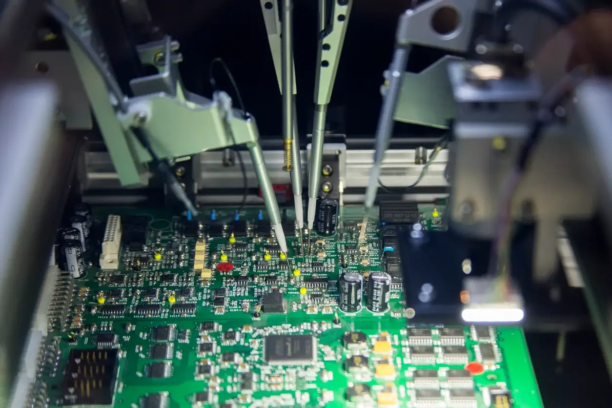
Flying Probe Testing uses software, files, and data from the PCB design. The probes move to reach the pads, vias, and components to be tested. The measured electrical response is compared to its expected value as determined by the PCB design files.
SUGA offers Flying Probe Testing in the same facility as fabrication, assembly, and testing. It is used to test prototypes, high-density designs, low-quantity orders, and complex PCB layouts that may require electrical testing before producing an ICT fixture. The test checks shorts, opens, component polarity, and component network connections. It identifies potential future design-change risks. SUGA can trace defects found on the probe bed to the specific panel, reflow profile, or layer build on the same day the defect is discovered because fabrication, assembly, and testing are closely integrated within the same supply chain.
How Board Data Becomes a Test Result
PCB design files are the basis for generating the test program. The design files contain the required information needed to create the test program. All expected measurement nodes must have physical access for the probe. A five-stage process exists for planning and executing a Flying Probe Test.
| Step | Input | Action | Output | Next Step |
|---|---|---|---|---|
| Design data loading | Gerber, BOM, ECAD, IPC-D-356B, ODB++, IPC-2581C / IPC-DPMX, or native ECAD | Convert design and netlist information into test coordinates and expected values | Testable node list and measurement plan | Confirm pads, vias, and netlist data are usable |
| Test program generation | CAD-based netlist and component data | Build a software test path without a custom bed-of-nails fixture | Flying probe test program | Update the program when the design changes |
| Probe positioning | 2–8 moving probes | Move probes sequentially to accessible pads, vias, or component nodes | Contacted test points | Continue only where geometry supports reliable contact |
| Electrical measurement | Resistance, capacitance, inductance, diode, polarity, continuity signals | Apply electrical stimulus and measure the response | Measured response for each net or component | Compare with expected values |
| Result evaluation | Expected vs. measured response | Flag opens, shorts, wrong values, reversed polarity, or mismatch | Pass/fail and defect-location signal | Route the defect pattern to coverage or risk review |
Turning Design Files Into Probe Paths
This includes Gerber, BOM, ECAD, IPC-D-356B, ODB++, IPC-2581C / IPC-DPMX, and other native ECAD design files used to provide the test data needed to build a node list, select measurement points, and determine the expected results of the electrical tests. As the prototype design changes, the test path can be updated in software in the event of a BOM or PCB layout update. A physical ICT fixture requires a different level of commitment.
Probe Movement and Measurement
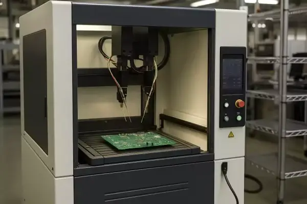
Probes sequentially contact the board one point at a time, contacting pads, vias, and component pins, applying a signal to each point, measuring the signal response, and then moving to the next accessible node.
The downside of sequential probing is that it is more time-consuming than fixtures. However, it provides your company with a viable test solution for prototype designs as well as low-volume manufacturing orders, while high-volume production often shifts away from the slower process of sequential probing in favor of a faster fixture-based process.
Result Evaluation
For the measured values from each probe to generate useful feedback, the tester compares each measurement against the expected value defined for the current measurement.
Whenever a measured electrical response falls outside the threshold defined by the user, the tester generates a defect signal.
What Can a Flying Probe Test Detect?
A Flying Probe test can successfully detect many different types of electrical defects at the board level, but the extent of detection depends on what the component being measured allows the tester to evaluate. The full set of standard checks, as provided by the SUGA Flying Probe test program, includes opens, shorts, continuity, missing or wrong parts, wrong values, polarity, and selected component signatures. Configuration-dependent tests execute once the configuration is adequate, including the equipment, program, and safety standards for executing those tests. If electrical testing requires powered, thermal, or frequency modes, testing then takes on a project-specific scope and must be evaluated on a project basis.
| Defect or Check | Detection Signal | Component or Net | Coverage Note |
|---|---|---|---|
| Missing components | No response at component nodes | Component placement and node response | Confirms electrical absence at the node; not a visual inspection |
| Wrong values | Measured value outside tolerance | Resistance, capacitance, inductance, semiconductor values | Applies to measurable components; tolerance window follows the program and device setup |
| Reversed polarity | Incorrect component characteristics | Diodes, LEDs, polarized parts, regulator signatures | A polarity and signature check, distinct from full functional validation |
| Solder shorts | Low resistance between isolated nodes | Isolated nets and adjacent nodes | Strong standard coverage when the nodes are accessible |
| Solder opens | High resistance or no continuity | Nets, connectors, PCB/PCBA network continuity | Based on design-file and netlist connectivity |
| Wrong parts | Measured characteristics mismatch | Component value or signature mismatch | An electrical mismatch check, not brand-level component authentication |
Opens and Shorts
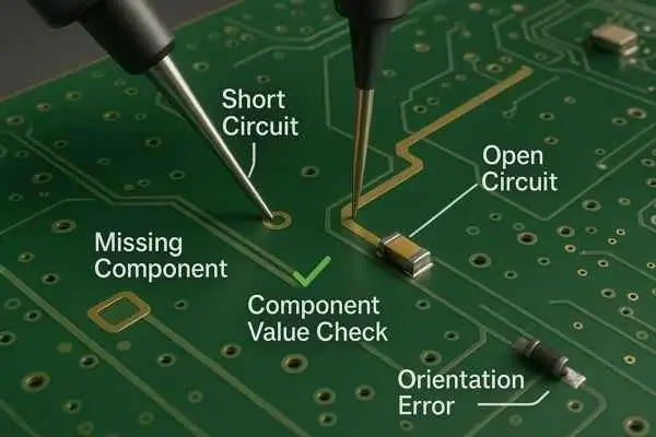
As electrical circuit boards are the base for connectivity, and since electrical conduction occurs through the internal layers or underneath the components of a circuit board, it is not possible to see shorts on a circuit board from the surface. Therefore, any detected shorts must be confirmed by comparing the measured node network against the design netlist.
Network connectivity is achieved with the help of the design file. When the netlist and the board data are in agreement, the tester will use the reachable nodes to verify the electrical network.
Component Value Checks
Value confirmation will work when an electrical component has a measurable value. Examples of measurable values are as follows: resistance, capacitance, inductance, fuse conductance, diode forward voltage, coil impedance, and connector shorts.
Make sure to verify which components you will be using a programmed tolerance window for, specifically for capacitance and inductance checks, as these checks will only be confirmed if your test program includes numerical limits for pass/fail. Board data will not indicate tolerances for these components.
| Test Item | What Is Measured | Coverage Type | Setup Requirement |
|---|---|---|---|
| Resistance | Value | Standard value check | Core measurable component example |
| Capacitance | Capacitance value | Standard value check when programmed | Runs only when tolerance limits are programmed into the test |
| Inductance | Inductance value | Standard value check when programmed | Runs only when tolerance limits are programmed into the test |
| Fuse | Conductivity | Continuity check | Pass/fail conductivity example |
| Diode | Conductance voltage | Polarity / junction behavior | Diode direction and response checks |
| Light Emitting Diode | Forward voltage/polarity; chromaticity, brightness, and saturation when optically equipped | Standard polarity check plus equipment-dependent optical mode | Polarity is standard coverage; brightness/chromaticity validation requires optical setup |
| Voltage Regulator | Forward voltage and reverse breakdown voltage | Component signature check | Powered or signature-style check with a defined setup |
| Photocoupler | Forward voltage and function response | Equipment-dependent function signature | Setup-dependent |
| Transistor (BJT) | PN junction voltage drop and function response | Semiconductor signature | Junction response check; full function depends on program coverage |
| MOSFET | Vds and function response | Semiconductor signature | Equipment-dependent function check |
| Relay | Coil impedance, NO/NC state, and function response | Electromechanical check | Relay nodes must be accessible and the program must support switching |
| Chip (IC) | Soldering, short-circuit, and partial function response | Solder / short / partial function | Not a full IC functional validation |
| Transformer | Coil inductive impedance and function response | Coil / inductive check | Coil impedance example |
| Connector | Short-circuit test | Connectivity / short check | Connector pin short example |
| PCB / PCBA | Full network connectivity per design file | Netlist-based connectivity | Strong core coverage when design data and access points align |
| Voltage converter chip | Output voltage | Powered voltage check | Requires powered setup and safety conditions |
| Frequency test | Output frequency of active crystal oscillator | Frequency mode | Requires frequency-capable setup and program support |
| Power-on test of logic chips | Logic response | Powered logic check | Optional mode outside base FPT coverage |
Polarity and Functional Signatures
Polarity and functional signature checks compare measured device behavior against the expected device response.
This check verifies reversed or mismatched parts when a measurable electrical signature can be produced.
This check is still different from a full functional test. A flying probe test could detect a signature mismatch without proving the circuit functions under operating conditions.
Equipment-Dependent Test Modes
Equipment-dependent test modes are available for advanced flying probe testing, provided the configuration meets the requirements of the project. SUGA can configure the equipment-dependent test modes.
| Mode | What It Supports | Dependency | Coverage Limit |
|---|---|---|---|
| PDM | Device-dependent defect detection | Tester option and program configuration | Advanced mode, not base coverage |
| HVS | High-voltage or specialized stimulus testing | Safety setup and tester capability | Tied to configured equipment |
| Micro-short detection | Detecting very small short-circuit signals | Measurement resolution and program setup | Optional precision mode |
| Capacitive coupling | Non-contact or capacitive behavior checks | Specific probe and measurement setup | Not applicable to every board |
| Thermal imaging | Heat-based defect observation | Thermal sensor integration | Separate from standard electrical probing |
| AOI integration | Combines visual and electrical defect coverage | AOI equipment and process pairing | Complementary mode, not FPT-only coverage |
Flying Probe vs. ICT
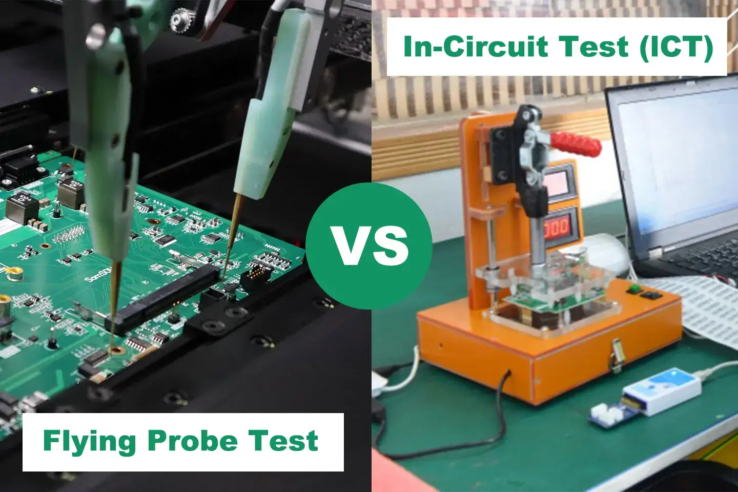
Flying probe testing and ICT solve different production problems. Use flying probe testing when the design is changing, the order is low-volume or high-mix, or the fixture cost is not yet justified. Use ICT when the design is stable enough to support a custom fixture and repeat volume makes faster per-board testing worth the upfront investment.
Because SUGA fabricates, assembles, and tests under one roof, moving from flying probe testing to ICT later does not mean re-explaining your board to a new vendor — the same design data and defect history carry over, which is part of what keeps the fixture ramp on schedule.
| Characteristic | Flying Probe Testing | ICT | Decision Impact |
|---|---|---|---|
| Test method | Point-by-point testing with moving probes | Pre-fixed probes for one-time testing | FPT supports changing designs; ICT rewards stable repeat layouts |
| Test speed | Slower | Faster; 10–100× faster benchmark | Speed advantage matters when repeat volume is high |
| Test coverage | Very high | High | Coverage depends on access, program, and equipment rather than method label alone |
| Upfront cost | Lower, no fixture cost | Higher; $2,000–$50,000+ fixture benchmark | Fixture cost must be spread across expected volume |
| Unit cost | Moderate | Lower | ICT can win after repeat quantity justifies the fixture |
| Flexibility | Excellent, adapted to different designs | Poor, requires specialized fixture design | Program updates are easier than fixture changes during NPI |
| Scenarios | Prototyping, low-volume production | High-volume production | Use FPT first, then move when design and volume stabilize |
Fixture Cost vs. Per-Board Cost
Review the costs associated with the fixture and how cost per board will look. Flying probe testing provides early engineering protection on money spent for early-stage prototyping while, for established production programs, ICT allows for the biggest return on investment due to the ability to amortize the cost of a fixture over many units.
Divide the fixture cost for ICT by the incremental cost saved per board, as calculated in the section "Speed vs Coverage" — the difference between the flying probe test time and the ICT test time. The quotient will yield a quantity of boards needed for the cost of the fixture to be recouped. Below that, flying probe testing will deliver a lower total cost due to the absence of having to recover a fixture investment. After that point, the increase in speed per board from the use of ICT will outweigh the cost of the fixture, especially with stable designs having high repeat demand.
Look at the example of 3,500 test points under the "Benchmark Example" below: on that design, flying probes take approximately 6 minutes to test per board, whereas once the ICT fixture has been built and debugged, it will take approximately 40 seconds to test per board. Therefore, the difference in time taken to complete each board tested is approximately 5 minutes per board; multiply that by your facility's per-minute test rate. Dividing the fixture cost by the cost saved per board will yield the order quantity needed for the ICT fixture to break even for the specific 3,500 test point design selected.
Test Speed vs. Coverage
Coverage planning is not replaced by the speed of a fixture.
While it is possible to achieve high coverage percentages with flying probe testing, it does not guarantee that every node is reachable, especially when dense PCBs have large numbers of nodes underneath BGA packages.
Design Change Flexibility
A flying probe testing program follows design changes easily. In contrast, a fixed ICT fixture will take much longer to reconfigure. For example, when BOMs, netlists, and pad access change during the NPI, it is much easier to implement a software change than to reconfigure the ICT fixture.
Benchmark Example: 3,500 Test Points / 750 Nets
| Method | Pitch | Setup/Learn Time | Test Time per Board | Selection Note |
|---|---|---|---|---|
| Fixture test | 0.020 inch fixture pitch | 30 minutes setup + 10 minutes debug | 40 seconds per board | Faster per board once fixture setup is justified |
| Flying probe test | 0.004 inch flying-probe pitch | 20 minutes learn time | 6 minutes per board | Better for fine pitch and lower-repeat work in this benchmark |
| Example board | 3,500 test points / 750 nets | 15 manufacturing panels example | Not a single test time | Benchmark logic, not a fixed switching rule for every project |
Flying Probe Testing Applications
Flying Probe Testing serves those who require electrical assurance before committing to a fixed fixture. Prototypes and R&D assemblies, low-volume and high-mix production, dense HDI PCBs, flexible and rigid-flex PCBs, multilayer connections, and selected RF and high-speed board evaluations are instances where Flying Probe Testing would apply. Each of these scenarios makes use of SUGA's corporate capabilities for design reviews, fabrication, and assembly; thus, any corrective action taken during testing does not need to leave SUGA's supply chain.
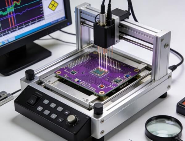
Prototype Electrical Verification
Prototype electrical verification has no fixed procedure. Prototype PCBs and PCBAs often change following the initial testing of the first prototype electrical results. The use of Flying Probe Testing allows the Engineering Team to evaluate the PCB and PCBA prototypes and to ascertain if there are open and short-circuit connections, component value discrepancies, incorrect part connections, and whether they will pass the initial electrical tests prior to spending time and money on the development of a test fixture. The Engineering Team can continue working on the design while the layout and BOM continue to be edited and modified. Common findings from the first article of prototype electrical testing are normally reversed polarity and unexpected open circuits; generally, these findings demonstrate issues with assembly quality or footprints, which means that the team can confirm their findings and repair the circuit, eliminating the need to respin the entire PCB or PCBA.

Low-Volume and High-Mix Production
Low-volume and high-mix orders will benefit from a configurable test program. Variants of boards can use a test program without needing dedicated fixtures for each layout. Switching between different board variations typically involves loading a new program rather than using a new fixture or swapping out hardware. For boards that will be produced in lower quantities, fewer than 500 boards often favors flying probe testing; 500–2,000 boards needs project cost analysis; and more than 2,000 boards often pushes the discussion toward ICT. The ranges mentioned above should be considered as decision logic and not limited to fixed quantities.
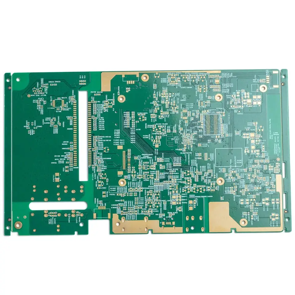
Dense HDI and Microvia Boards
A densified HDI board can use a flying probe test when the initial access point has been established. Things like fine-pitch components, microvias, blind vias, buried vias, and fine contact-pad geometries can create opportunities for probers to find the pin pads. Often, there are no traces of the pins on the inner layers that could be probed directly, which would typically be the case with blind vias or buried vias. As such, if the probe cannot directly access the inner layer, it must use the closest pin pad to it, which is confirmed by reviewing the netlist, not the actual location of the inner layer via. Therefore, netlist alignment is equally important as pad size on densified HDI boards.
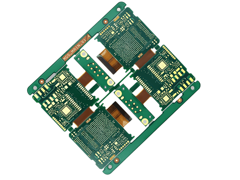
Flex and Rigid-Flex Assemblies
When a flexible and rigid-flex assembly has been constructed, there is a mechanical challenge added to the operational testing procedure. Sensitive areas of the board generally will require either some sort of support or an alternative method of contacting them. The potential risk is often not with the condition of the electrical signal obtained from the probe, but the amount of force applied to the assembly during the test procedure that can affect the integrity of the region. The most effective way to combat this problem is to provide localized support underneath the flexible area during the test process rather than relying only on the borders of the PCB to adequately stabilize the flex.
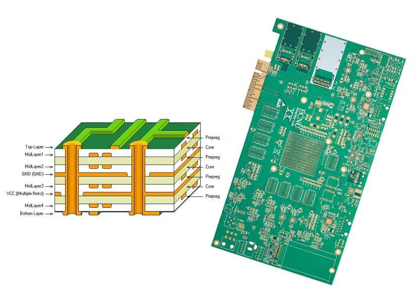
Multilayer Connectivity Checks
Most multilayer PCBs will require the use of a netlist-based connectivity check. The flying probe software will compare the electrical connectivity from the accessible nodes to the design data to identify any differences in connectivity across the PCB's electrical network. Vias will provide access to the inner layers; however, they will not eliminate the requirement of having accurate design data available prior to beginning the test. An outer-layer via will confirm the presence of the inner layer's net and that it is intact without the probe ever contacting the inner copper directly.
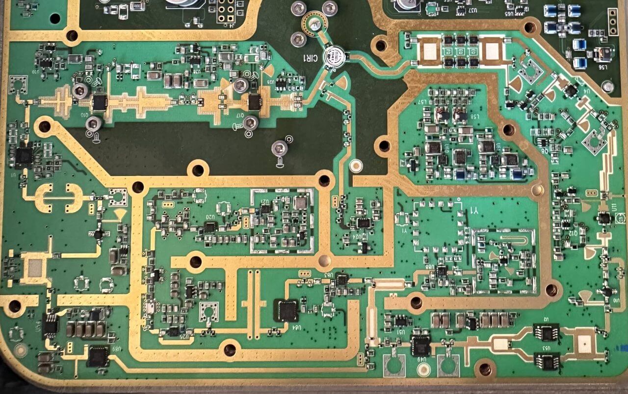
RF or High-Speed Boards With Test Limits
Most high-speed and RF PCBs will continue to use the flying probe method of verifying the board via an electrical check of the PCB's layers. The tests performed via the flying probe testing method will provide the ability to check for shorts, continuity to ground, and opens in the PCB, and to use various probe modes to check for manufacturing faults. The limitation of flying probe testing for PCBs is that it checks whether the PCB electrical net was built correctly; it will not validate RF or high-speed circuit performance, as such test methods will require other methods of verification such as TDR or VNA. However, flying probe testing verifies that a PCB was manufactured correctly, while other methods validate that the PCB functions correctly at its design speed.
Designing Test Access for Dense Boards
A dense PCB may be an acceptable candidate for using flying probe testing as long as the tester is able to reach reliable conductive targets and the program has trust in the design data. The key factors that will affect whether a dense PCB is a viable candidate for using flying probe testing methods include pad, via, supporting structure clearance, component height, and netlist alignment. A dense PCB will need to have sufficient margins so that the correct node can be contacted without damaging or impacting any features adjacent to the targeted pin pads or generating false results.
| Check Item | What It Proves | Data | Access Note |
|---|---|---|---|
| Reachable pads or vias | The probe has a conductive target without damaging nearby features | Exposed pads/vias; 80 µm standard contact pad | Reachability comes before minimum values |
| Pitch and spacing | Adjacent targets support probing without shorting or collision | 0.004 inch / 0.10 mm FPT pitch vs. 0.5 mm ICT pitch | Geometry and equipment conditions |
| Contactable pad limit | The board supports stable probe contact | 30–70 µm fine-pitch rows; 80 µm standard rows | Fine-pitch equipment reaches smaller pads than standard equipment — full comparison below |
| Netlist and design data alignment | Program coordinates and expected electrical values match the board | IPC-D-356B; ODB++ / IPC-2581C / IPC-DPMX; native ECAD | Engineering data alignment, not a request list |
| Component height and board support | Probe path and contact force remain stable | UUT size, device height, flex reel width | Mechanical access affects electrical test reliability |
How Small Can Test Access Be?
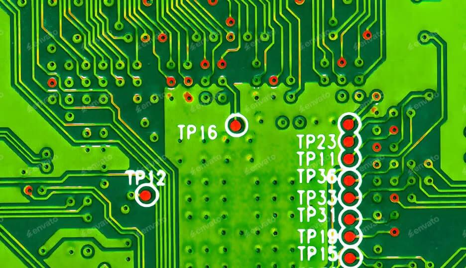
The smallest possible access point does not equal the best access point. Use the following table as a benchmark for your access point capabilities, and allow for additional margin for pad shape, solder mask, nearby components, probe angle, and board support.
Fine-pitch flying-probe systems and ordinary flying-probe systems are two separate pieces of equipment, not two separate numbers for the same machine. A fine-pitch system is capable of accessing contacts on a pad down to 30–70 µm, whereas an ordinary system reaches down to 80 µm. SUGA will only quote for what your design requires in terms of pad geometry.
| Parameter | Benchmark Value | Practical Use | Setup Note |
|---|---|---|---|
| Minimum Continuity Resistance | 0.1 Ohms | Electrical continuity sensitivity benchmark | Baseline equipment sensitivity, not a required design target |
| Maximum Test Voltage | 1000 Volts | Electrical stress boundary benchmark | Configured per board and safety requirements; not applied by default |
| Maximum Isolated Resistance | 25 MΩ – 2 GΩ | Isolation measurement range benchmark | Reflects equipment capability; actual reading varies by net |
| Electrical Test Pitch (Fixture) | 0.020 inch | Fixture access comparison | Used for FPT vs. fixture access comparison |
| Electrical Test Pitch (Flying Probe) | 0.004 inch / 0.10 mm | Fine-pitch probing benchmark | Achievable pitch also depends on pad geometry and design margin |
| Contactable Pad, Fine-Pitch (min) | 30–70 µm | Fine-pitch equipment tier | Applies on fine-pitch flying-probe systems only |
| Contactable Pad, Standard (min) | 80 µm | Standard equipment tier | Baseline tier for pads above the fine-pitch range |
| UUT Size | Up to 1524×610 mm on large-format equipment | Equipment envelope example | Equipment table context |
| Flexible Circuit on Reel Width | Up to 190 mm on flex-handling equipment | Flex handling context | Equipment boundary context |
Probe Clearance Around Pads and Vias
In addition to being small enough, a good target for flying probe testing must remain stable while applying contact pressure, as well as have sufficient distance from other nearby parts and conductors to prevent false shorts or mechanical obstructions.
Flex and rigid-flex assemblies require added attention because they can flex or move and therefore require additional considerations regarding probe angle, component height, and board support.
CAD and Netlist Alignment
A failure in physical access may result from the probe contacting the board, yet receiving an incorrect electrical signal. The CAD data, netlist, component positioning, and any generated comparative data must all connect back to the same electrical node before any measurements can be trusted to be accurate.