Upload BOM & Gerber
-
Mobile: +86 13312967631
-
Email: sales@sugaintl.com

Rogers & PTFE RF PCB
Rogers and PTFE RF PCB fabrication in China, built around Rogers PCB material properties, hybrid stackup control and manufacturer-level PTFE process control
SUGA fabricates Rogers RO3000/RO4000, RT/duroid and hybrid Rogers-FR4 RF PCBs — 24-72h prototype turnaround, controlled RO3003 process Dk 3.00±0.04, and verified stackup, drilling and RF proof for radar, mmWave and satellite-grade boards.
24–72 HrsPrototype Turnaround
Dk 3.00 ±0.04RO3003 Process Control
UL94 V-0RO4350B Flame Rating
1–10 PcsPrototype-Ready Volume
RF And Microwave PCB Fabrication With Rogers PTFE Materials
RF microwave PCB projects start by selecting a laminate material. However, the laminate will only work as intended if the board geometry, copper design, stackup, and volume plan all match. SUGA assists customers working with Rogers PTFE laminates by checking the laminate, confirming stackups, and matching project-specific RF laminate fabrication needs.
A low-loss RO3000 laminate, a process-friendly RO4000 laminate, and a hybrid Rogers-FR4 stackup answer different engineering questions. The practical decision is whether the project needs lower loss, tighter Dk stability, better moisture behavior, flame-rating support, or a controlled hybrid structure. The material tables, cost analysis, and prototype-to-production preparation keep those figures in context so the material selection can be tied to stackup, cost, and schedule instead of treated as a standalone datasheet decision.
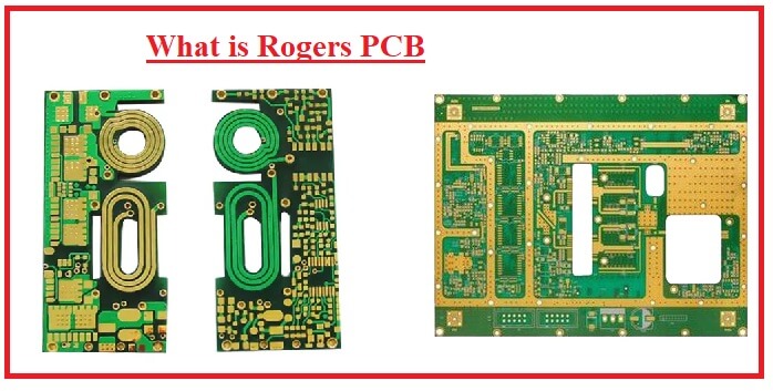
What Is Rogers PCB Material?
Rogers PCB material is a family of low-loss laminates that provide better stability in electrical performance than standard FR-4 offers when RF, microwave, mmWave, or high-speed circuits are designed. When selecting material, four different factors need to be evaluated to determine which material family is most appropriate: dielectric loss, Dk stability, moisture behavior, and impedance repeatability.
Rogers PCB Material Definition
In PCB work, Rogers PCB material refers to a high-frequency laminate used for lower dielectric loss and tightly controlled electrical performance. For example, RO3003 is positioned on the low-loss side of the spectrum with a Df value of 0.0010 measured at 10 GHz; RO4003C and RO4350B sit higher at 0.0027 and 0.0037, both of which are appropriate for many commercial RF designs because their processing remains closely aligned with what a standard PCB manufacturing facility is accustomed to.
Why RF Boards Use Low-Loss Laminates
For RF designs that operate at a relatively low frequency, standard FR-4 can be acceptable. However, as frequencies increase, insertion loss, phase shift, and impedance drift begin to erode the available design margin, and even a slight change in the material used for fabrication can have a significant impact on antenna gain, radar sensitivity, or the repeatability of a matched RF path. Low-loss laminates such as Rogers or PTFE materials are used when the board is intended to maintain signal behavior rather than only act as an interconnect between components.
Material Choice Starts With Fabrication Risk
Material selection should be directly tied to the manufacturing method before the stackup is determined. The RF requirements may require more strictly defined copper profiles or tighter fabrication checks than the datasheet indicates. For SUGA projects, material and fabrication discussions should start together around the actual RF performance required.
Rogers PCB Material Types
Several families of Rogers PCB materials exist to support different electrical engineering and manufacturing needs rather than competing on a single low Df parameter. RO4000 materials support commercial RF designs that require stable electrical performance while using common manufacturing paths. RO3000 materials and RT/duroid materials have been developed to achieve lower loss, PTFE behavior, and stronger process discipline. TMM laminates are used to support higher Dk for small microwave designs. The more relevant comparison relates to which family has the lowest fabrication risk associated with the specific circuit geometry rather than which family has the lowest Df.
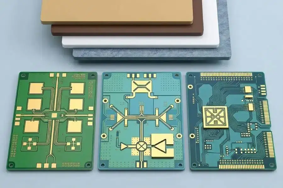
| Material family | Example materials | Material data | Best-fit use |
|---|---|---|---|
| RO4000 | RO4003C, RO4350B, RO4835, RO4360G2 | RO4003C process Dk 3.38 ±0.05, design Dk 3.55, Df 0.0027; RO4350B process Dk 3.48 ±0.05, design Dk 3.66, Df 0.0037 | Commercial RF, antenna feed networks, hybrid stackups |
| RO3000 | RO3003, RO3006, RO3010 | RO3003 process Dk 3.00 ±0.04, design Dk 3.16, Df 0.0010, CTE 17/17/24; RO3006 Dk 6.15, Df 0.0020; RO3010 Dk 10.20, Df 0.0022 | Radar, mmWave, compact RF, low-loss circuits |
| RT/duroid | RT5870, RT5880, RT6002, RT6006, RT6010 | RT5880 Dk 2.20 ±0.02, Df 0.0009, moisture 0.02%, thermal conductivity 0.20 W/m/K; RT6002 Dk 2.94, Df 0.0012, CTE 16/16/24 | Ultra-low-loss microwave and long RF paths |
| TMM | TMM3, TMM4, TMM6, TMM10, TMM10i | Design Dk range 3.45 to 9.9; Df 0.0020-0.0023 | Compact microwave circuits and high-Dk layouts |
RO4000 Series
RO4000 materials are the most common suitable materials available for commercial RF circuit boards. Between the two common grades, the difference in loss (Df 0.0027 for RO4003C vs. 0.0037 for RO4350B) is not substantial enough to decide which material is used by itself; the flame rating will usually dictate which material is used. According to the RO4350B datasheet, it has a UL94 V-0 material rating, while RO4003C does not. When the circuit board is incorporated into an enclosure with its own flammability requirements, that one difference can outweigh the loss number; that misunderstanding occurs when RO4003C and RO4350B are treated as interchangeable BOM material line items.
RO3000 Series
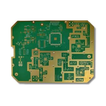
RO3000 materials are ceramic-filled PTFE alternatives for designs that require lower loss or more precise Dk control. The low-loss anchor for RO3003 is Dk 3.00 ± 0.04, Df 0.0010. RO3006 (Dk 6.15) and RO3010 (Dk 10.20) are used in more compact RF geometries where higher Dk materials can save board real estate rather than improve absolute loss performance. For that benefit to be realized through RO3000 materials, the fabrication method must be confirmed before the board stackup is finalized, meaning the part number alone is not enough on the stackup drawing, and RO3000 materials require different procedures for drilling and hole-wall preparation than RO4000 materials.
RT/duroid With TMM Materials
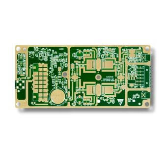
RT/duroid and TMM represent the more specialized Rogers line of materials, including RT5880 (Df 0.0009, moisture absorption 0.02%) for ultra-low-loss microwave paths and RT6002 (Dk 2.94, Df 0.0012), with a matched in-plane CTE of approximately 16 ppm/°C, which helps plated-through holes remain stable during thermal cycling. RT5880 has a significantly higher CTE, creating different thermal-cycling behavior, which often leads to the selection of RT5880 and RT6002 for different uses within the same product family. RT/duroid offers multiple flame-rated grades, although not every grade carries the same UL94 rating; for example, some ceramic-filled RT6006/6010 grades are rated V-0, while RT5880 and RT6002 are often supplied without a UL94 rating in their standard TDS. Projects that specify flame-rated materials must verify the specific grade of RT/duroid or TMM material, rather than assume that products from the same family behave uniformly. TMM provides higher Dk for microwave circuit applications, allowing for further reduction in circuit size. However, circuit layouts still need to adhere to impedance geometry, copper balance, and thermal limitations.
PTFE vs. Hydrocarbon Ceramic Laminates
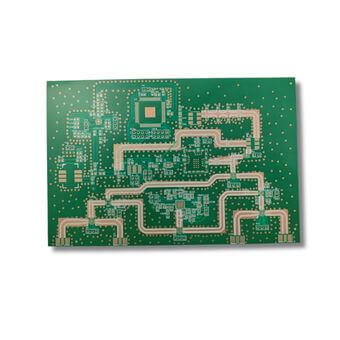
PTFE is a dielectric material base, but not every Rogers laminate uses PTFE. RO3000 and RT/duroid-style laminates use PTFE as their dielectric material; RO4000 material is hydrocarbon ceramic, and this is why it processes closer to a standard FR-4 line.
| Decision point | PTFE-based Rogers materials | Hydrocarbon ceramic laminates | Decision meaning |
|---|---|---|---|
| Electrical reason | Very low loss, stable RF behavior, useful for mmWave and long RF paths | Balanced RF performance with more familiar processing | The choice follows the RF target, not the material name alone |
| Fabrication behavior | More sensitive drilling, hole-wall preparation, plating and lamination | More familiar path for many PCB shops | PTFE changes the process path |
| Cost pressure | Usually higher material and process cost | Often better cost-performance balance | Cost belongs to material, process and verification together |
| Verification need | More likely to need coupons, TDR, VNA or S-parameter checks | Still needs impedance and stackup control | Test depth follows the project requirement |
What PTFE Changes In PCB Fabrication
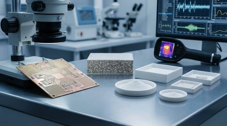
PTFE affects PCB manufacturers most by changing how they manage the board, rather than by changing any individual electrical specification. While a facility that is capable of producing high-quality FR-4 may be capable of producing a high-quality PTFE PCB, it is not unusual for such a manufacturer to find it challenging to produce a PTFE PCB if the facility does not have separate checks for PTFE hole-wall preparation and copper adhesion, since the surface chemistry of PTFE resists the same desmear chemistry used on epoxy resins.
When Hydrocarbon Ceramic Materials Are the Simpler Path
RO4000 family materials can perform adequately for typical RF antenna applications without requiring the specialized processing needed for PTFE materials. Commercial RF modules and mixed-signal electronics may be built with either RO4003C or RO4350B materials and have their dielectric loss and Dk parameters remain stable using a fabrication path commonly used by PCB manufacturers.
When PTFE-Based Rogers Materials Are Worth It
Additional processing steps for PTFE-based materials can be costly, so the cost should match the RF requirement before the project commits to the material. If a project requires PTFE-based materials for performance reasons, the extra processing expense is worth it when project requirements warrant the extra cost. PTFE materials designed and produced by Rogers offer strong dielectric loss and Dk characteristics for mmWave, radar, satellite communications, and compact microwave applications. RO3003, RT5880, RT6002, and RT6010 cover different mmWave, radar, satellite communication, and compact microwave needs through their Dk, Df, and process behavior.
Rogers PCB vs. FR-4
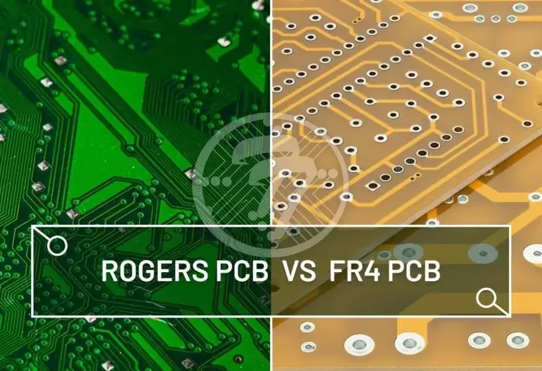
The increased cost associated with Rogers PCB materials results from the fact that standard PCB manufacturing processes will not provide optimal performance when the project requires dielectric loss, Dk, insertion-loss stability, or RF validation.
| Comparison point | FR-4 | Rogers / PTFE RF materials | Practical decision |
|---|---|---|---|
| Dielectric loss at 10 GHz | Df 0.017-0.025 | RO4350B Df 0.0037; RT5880 Df 0.0009 | Use Rogers when loss becomes part of the RF budget |
| Moisture behavior | Higher risk for RF stability | RO4003C water 0.04%; RO4350B water 0.05%; RT5880 water 0.02%; RT6002 water 0.02% | Low moisture helps impedance and phase consistency |
| Process familiarity | Strong fit for digital, power and lower-frequency support layers | Depends on family; RO4000 is easier than PTFE-based material paths | Hybrid stackups can use both materials |
| Cost | 1x baseline | Higher relative material cost | Use Rogers only where the RF path needs it |
Signal Loss At Higher Frequency
While the Df of FR-4 at 10 GHz between 0.017 and 0.025 remains suitable for digital and lower-frequency circuits, this becomes less suitable for radar, microwave links, and matching networks that require lower-loss materials and repeatable phase. The performance gap between FR-4 and laminates such as RT5880 contributes to whether a link budget can be closed.
Moisture-Driven Dimensional Stability
The moisture absorption numbers in the chart above have less significance when expressed as percentage rates and are more of an indicator of the potential for long-term phase drift than anything else. During a common humidity test (85°C/85% RH for an extended period) for RF qualification, a laminate with a moisture absorption rate of 0.04-0.05% can produce more impedance and phase drift than a laminate with 0.02% moisture absorption. Water absorption changes the effective Dk across the laminate. While the percentage difference looks better on the datasheet for RT5880 and RT6002 compared with RO4350B, project teams specify RT5880 or RT6002 over RO4350B because they can cause less detuning of the matched network after several months of service. Project teams should check the actual drift measurements against SUGA's qualification data before estimating any guarantees.
When FR-4 Still Makes Sense
FR-4 is still the best laminate for many RF applications. For low-frequency circuits, digital circuits, and power distribution, FR-4 is often adequate, as there are usually only a few microwave paths in each hybrid stack-up. Hybrid stack-ups can use FR-4 as mechanical support for Rogers material only on the RF path, making them a better cost decision than all Rogers material on an entire microwave PCB.
Cost Drivers For Rogers And PTFE PCB Fabrication
The cost of Rogers and PTFE PCBs is not a simple single-material-price issue. Materials, laminate thicknesses, copper weights, layer counts, hole structures, and special considerations for hybrid or multilayer constructions all have an impact on pricing — for example, an RF path that extends into a hybrid stack-up will not be priced the same way as a fully dense multilayer PTFE construction.
| Driver | Cost Range | Why it changes cost |
|---|---|---|
| Relative material family | FR-4 1x; RO4003C 5x-7x; RO4350B 5x-8x; RO3003 8x-12x; RT5880 10x-15x; RT6002 12x-18x | The laminate itself sets the first cost step |
| Hybrid stackup | Rogers RF layers plus FR-4 digital, power or support layers | Cost is focused where RF performance is required |
| PTFE process path | Drilling, hole-wall preparation, lamination and plating controls | Process control adds time, setup and scrap sensitivity |
| RF verification | Coupon, TDR, VNA, S-parameter checks when needed | Measurement depth follows the project risk |
Relative Material Cost
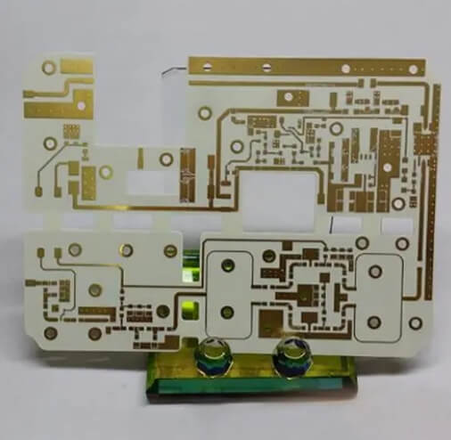
The above table does not represent final material pricing; it is an initial filter for selecting the best material option. Final material selection depends not only on frequency but also on the margins that remain in the system design. A system operating at 24-40 GHz with 3 dB of margin is often adequate to remain with either RO4003C or RO4350B material in most cases; however, if the system is designed with only a 0.5 dB budget, it will be necessary to use either RO3003 or RT5880 material regardless of the additional cost passed on to the customer, because there is no loss available to spend. Panel utilization also affects the total material cost per individual board. The additional cost associated with a poorly designed panel can exceed the cost savings from using a lower-grade material. Even when the table is used as an initial reference for material selection, the quotation should also take panel utilization into account.
Hybrid Stackup Cost Control
A hybrid stackup incorporates Rogers materials on the RF path and FR-4 in the digital, power, or mechanical layers, thus protecting the electrical performance of the board while keeping the overall board cost from moving into the highest material cost range. The downside of a hybrid stackup is that there are many factors that must be taken into account when designing the stackup: bonding, CTE matching, registration, impedance coupons, and material availability. Failure to define these elements before the stackup is finalized will lead to increased costs.
Verification Cost In RF Fabrication
Because RF behavior checks add cost, the acceptance method — coupon, TDR, VNA, or S-parameter — needs to be preset rather than derived afterward. The cost differential arises from the selected laminate, build difficulty, and how far that check must go.
How To Choose Rogers PCB Material?
Material selection should occur after defining the target electrical performance at frequency, insertion loss, phase stability, board size, laminate thickness, and impedance. These criteria define the family of possible materials before entering a discussion of part numbers.
| Frequency Range | Material direction | Why it fits |
|---|---|---|
| 1-6 GHz | RO4000-style materials often suit this range | Balanced RF performance and easier fabrication path |
| 6-20 GHz | RO4000 or selected lower-loss materials | Loss, thickness and copper start to matter more |
| 20-40 GHz | RO3000 or RT/duroid options become stronger candidates | Phase and insertion loss become harder to ignore |
| 40-77 GHz | RO3003 or comparable low-loss material paths deserve attention | 77 GHz radar needs stable Dk and low loss |
| 77 GHz+ | Specialized low-loss material path with verification planning | Material, copper and measurement path must be planned together |
Start With Frequency And Loss Budget
Frequency is the first filter, but the loss budget, RF path length, trace geometry, and desired measurements should drive the final material selection. If you wait until later to change from the original material to another material, you may need to change trace geometry, copper selection, and associated costs all at once. Frequency is a useful starting filter, not an absolute measure of the best material.
Match Dk/Df To PCB Geometry
The Dk and Df values of the manufacturing process and the design process are not interchangeable. The process value is meant to support material acceptance testing; the design value is used to support field solving and trace geometry. When working with very fine RF traces or controlled-impedance launch conditions, both Dk values should be checked against laminate thickness, copper roughness, and impedance targets.
Check Flame Rating And Thermal Limits
Moisture content, thermal conductivity, CTE, flame rating, and compatibility with lead-free solder are all relevant to the material decision. RO4350B has a UL94 V-0 rating on the datasheet, RO4003C is non-FR, and for the RT/duroid product family, flame rating may vary by grade, not by family, so this check should not be skipped based on assumption. A UL94 rating applied to the base laminate does not automatically certify that the finished PCB meets the project flame rating; the PCB still requires its own build-level documentation. A material can electrically fit a project and still miss some requirements if this step is omitted.
Confirm Fabrication Verification
The final laminate decision will determine how the PCB is fabricated. A laminate material can appear to meet the electrical performance requirements but may also introduce yield or repeatability issues in the fabrication process unless the laminate properties match the process used for production; use a supplier-fit check to establish this.

RF Microwave PCB Manufacturing
An RF PCB manufacturer should be evaluated based on laminate handling and fabrication evidence rather than the mere inclusion of the term “Rogers” in the list of capabilities. The following checklist includes the manufacturing controls used to determine if the final manufactured board represents the design intent.
| Manufacturing control | What must be controlled | Why it matters |
|---|---|---|
| Material handling | Incoming laminate control, lot traceability, storage and surface protection | Low-loss laminates can be sensitive to handling and surface condition |
| Stackup and copper | Hybrid bonding, copper distribution, impedance targets | The RF path needs stable geometry and predictable dielectric behavior |
| Drilling and plating | Controlled drilling, hole-wall preparation, copper adhesion and plating checks | PTFE and low-loss materials can expose weak hole-wall processes |
| RF verification | Coupons, TDR, network analyzer or S-parameter checks when needed | Continuity alone does not prove RF behavior |
Material Handling For Stable Stackup
RF behavior can be modified before etching due to surface conditions, bonding conditions, and storage conditions that affect the assumed copper and dielectric conditions. When making hybrid Rogers-FR4 boards, RF and support substrates have to move through one matched build. Fabrication must match both the dielectric and copper conditions, not stack independently sourced materials together without matched control.
Hole-Wall Plating After Drilling
For PTFE-based laminates and low dielectric loss laminates, drilling and preparing the hole wall can be more sensitive than with other laminates, given that the key question is whether the selected preparation method will produce copper adhesion that survives the build cycle rather than only electrical continuity on the day it was drilled. If an alkaline permanganate desmear or CF4/O2 plasma method is selected, these methods can be used in the build cycle only if the fabrication method supports them. Neither procedure can be applied universally to all Rogers laminates.
RF Verification For Impedance Control
RF verification should mirror the end-use application, the construction complexity, and the level of test evidence needed for RF performance through the build process. Continuity testing does not provide adequate confirmation of RF performance, so the test depth should follow the input frequency, RF path length, and anticipated end-use risk of the product using Rogers laminates. SUGA matches laminate, geometry, quantity, and measurement plan to the fabrication and test controls each project actually needs.
RF PCB Application
Rogers products have many applications, but each circuit type has a different reason for using the product: a 5G antenna board is concerned about phase and repeatability, while a power amplifier board is much more concerned about heat, copper, and loss.
5G Antenna PCB
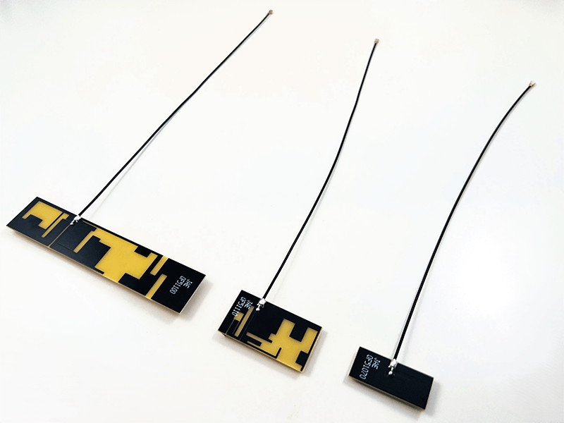
RO4000 material can provide suitable performance for many commercial 5G antennas. A lower-loss path may also be required for mmWave applications, with the key failure mode being not the continuity of any one particular net but array-to-array drift. Small differences in Dk or copper roughness between elements can cause beam-pointing error once the array has been assembled. mmWave arrays are specified with tighter Dk tolerance than the single-panel process alone; the difference in Dk between elements can combine across numerous elements to produce more beam-pointing error than is allowed within the antenna link budget. Exact Dk-to-beam error depends on the array size and must be confirmed against SUGA’s incoming-material batch data before being quoted as a specification.
Automotive Radar PCB
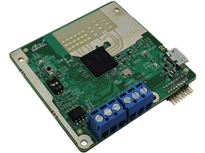
Automotive radar applications are trending toward lower loss products and stable Dk. RO3003 material’s Dk of 3.00 ± 0.04 and Df of 0.0010 are good matches for 77 GHz applications. The main concern with this application is the thermal cycling that occurs in an automotive under-hood location: RO3003’s matched 17 ppm/°C in-plane CTE allows plated-through-holes to be maintained through repeated thermal cycles of –40°C to +125°C that would cause the via barrels of a mismatched material to fail before the rated service life of the automotive radar application is completed.

Satellite Communication PCB
Satellite boards need both low loss and low moisture absorption over the long RF path; RT5880 material with a Df of 0.0009 and moisture absorption of 0.02% is a good fit for this application. A potential problem with using unfilled PTFE such as RT5880 to produce multilayer satellite boards with high-aspect-ratio plated-through-holes is that it has much higher Z-axis CTE than ceramic-loaded PTFE such as RT6002. This pushes many designs toward RT6002 due to the Z-axis expansion difference between unfilled PTFE and ceramic-loaded grades, even though RT5880 has lower loss than the ceramic-loaded grade. Equipment-level qualification of space-qualified materials is conducted using the program’s qualification process and is separate from PCB fabrication.
Aerospace And Defense RF PCB
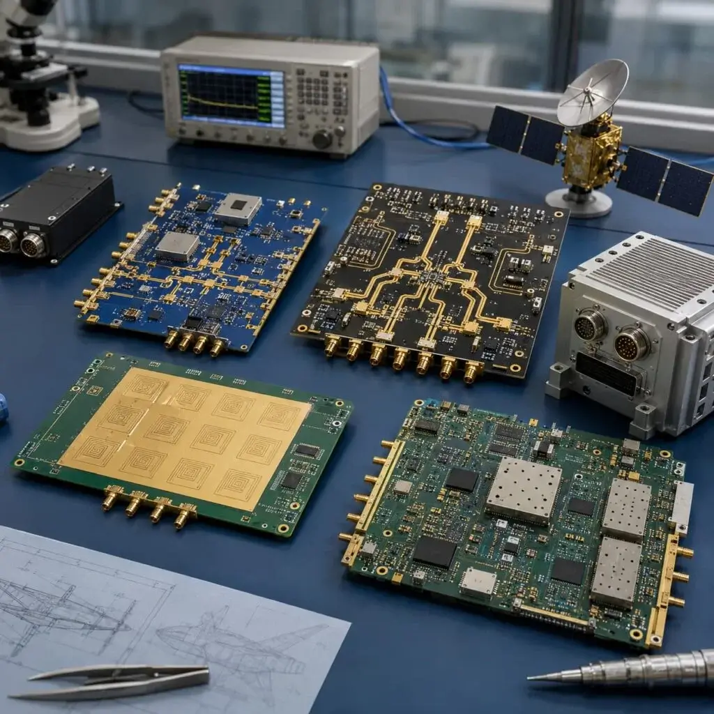
Aerospace and defense PCBs require material documentation, PTH quality, and phase behavior as contract deliverables, rather than relying solely on best practices. The pitfall specific to this category is that if a PTFE PCB is stored in humid conditions before assembly, moisture in the PCB can outgas during the lead-free reflow process. This can result in hole-wall micro-blistering that passes initial electrical testing but fails under later thermal cycling or burn-in screening. A pre-reflow bake-out step and documented storage humidity should be part of the material handling requirements, in addition to the laminate material.
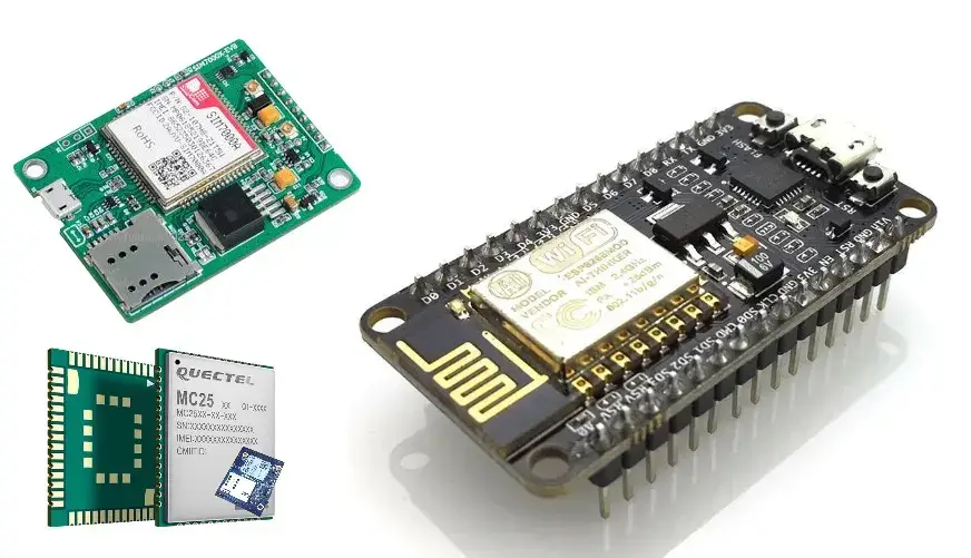
IoT RF Module PCB
The most significant concern with IoT RF module PCBs is antenna matching. However, a designer needs to determine whether it is necessary to specify more costly PTFE material to provide stable, low-loss RF performance, or whether RO4000 materials or a hybrid stackup will suffice for commercial IoT RF module production. The decision point is whether low-loss laminate areas are needed where the antenna and matching networks are located. For a hybrid design that isolates the antenna feed into a small island of RO4000, the RF performance can match that of a full Rogers board at a fraction of the cost. The isolated feed area is usually much smaller than the total board area on a compact IoT module, so a hybrid solution will normally be less expensive than upgrading to a full-board material for each unit. The size and cost differences must be calculated for each layout and should not be assumed without modeling.
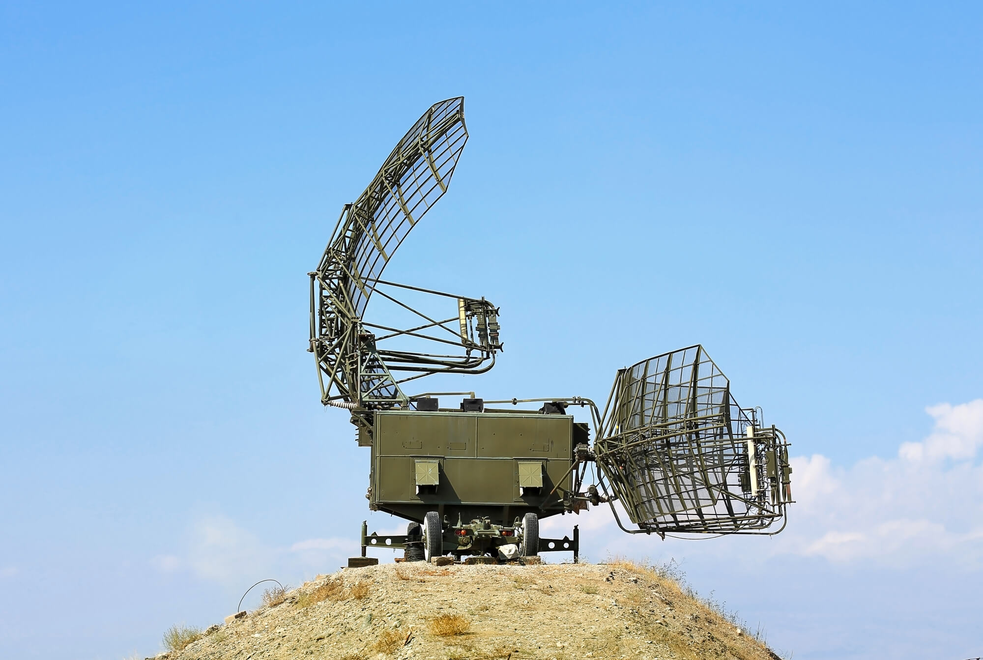
Phased Array Radar PCB
When constructing a phased array radar PCB, consistency across all channels is paramount. Copper roughness, Dk stability, and trace geometry of each PCB element directly affect phase behavior across multiple PCB elements. Each material option should be checked against loss expectations and size requirements to understand how these requirements fit into the calibration settings designed around each material, including RO3003, RT/duroid, and TMM.
When building a phased array radar, the pitfall is when materials used mid-array are different, even if they are considered electrically similar, because the swapped material can create a significant phase difference compared with the Dk stability curve used for calibration. A mid-build material swap creates greater risk for larger arrays than smaller arrays because the cumulative phase error across all elements degrades sidelobe level more rapidly than main-beam gain. It should be viewed as a re-calibration trigger rather than a standard substitution when material or lot changes occur in the middle of the build process.
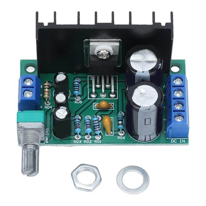
Power Amplifier PCB
PCB power amplifiers use the relationship between RF loss and heat in a manner that other applications do not; copper weight, via design, and plated-through-hole reliability can matter as much as the Df value. The real basis for comparing how well the materials transfer heat from the amplifier die is described in the thermal conductivities of TMM at 0.70 to 0.76 W/m/K and RT6010 at 0.86 W/m/K. Sizing the thermal via field for the actual thermal conductivity of the laminate, instead of using a previously established via pattern from a different laminate with better thermal conductivity, is one major common pitfall.
RFID Wireless Tag PCB
Although RFID boards are often extremely cost-sensitive, antenna geometry must have repeatability at very high panel density. The specific pitfall for RFID boards lies with thin-panel warpage; to achieve tag-level cost targets, RFID boards are frequently manufactured using extremely thin, heavily panelized construction with ceramic-filled or PTFE materials, which can increase susceptibility to warpage. Warpage will not manifest through individual unit impedance testing; panel-level flatness control using a dedicated fixture or panel flatness gauge method, rather than sample testing alone, is more important than the Dk value of the material. Specific thickness and warpage tolerances should be confirmed against SUGA’s panel specification for the target tag size, especially when ceramic-filled or PTFE materials are compared with a similar FR-4 panel.
Medical RF Equipment PCB
The medical RF equipment market includes monitoring, imaging, and compact RF front-end equipment. Traceability, cleanliness, stable impedance, and documentation will dictate whether a board can move from prototype to controlled production. One of the major pitfalls with medical RF equipment is coating compatibility; the low surface energy of PTFE, one of the main reasons for its high level of RF performance, makes it difficult to validate adhesion between conformal coatings, staking materials, and PTFE compared with FR-4. The coating process for a medical RF board must have its own adhesion validation. For example, pieces are usually run through a peel-strength test after going through the same sterilization cycle that the final products will undergo, eliminating the possibility of reusing coating-validation data from a standard production run. Device-level regulatory approval, including ISO 13485 or FDA-related processes, remains under the OEM’s quality system rather than PCB fabrication capability.
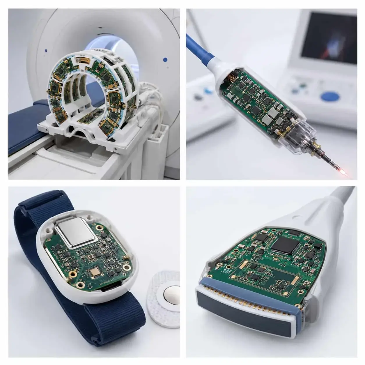
Rogers PCB Prototype To Production
Rogers or PTFE RF PCBs move through three build steps. First, the prototype build tests the material assumption. Next, low-volume production checks material repeatability. Lastly, repeat production preparation connects material traceability, RF testing, and delivery checks to ensure the boards maintain consistent reliability and quality records.
| Stage | Planning signal | What should be learned |
|---|---|---|
| Prototype learning | 1-10 boards; 24-72 h signal when the material and process allow it | Whether laminate choice, drilling, impedance and RF checks behave as expected |
| Low-volume validation | 10-1,000 boards signal | Whether the process repeats across a controlled quantity |
| Repeat production planning | Stable material lot, stackup, verification level and delivery planning | Whether lot control, panel use, verification and delivery planning are stable |
Prototype Learning
The prototype build checks whether the chosen materials, impedance targets, and test methods are compatible with one another. The 24-72 hour window is a guideline, not a rule; however, there are two factors that can push prototypes past their expected timeframe for production. The first is PTFE hole-wall preparation, which needs more process time than FR-4 drilling, and the second is scheduling production runs around other jobs that are already in progress. Because of this, projects with a strict specification for hole-wall configuration or an expedited production schedule should take the long end of that window into account.
Low-Volume Validation
The low-volume stage, for example a 10-1,000 board run, verifies the ability to manufacture within a defined volume rather than simply stating that the process has been validated by producing one prototype. This is also where many of the cost surprises associated with a production run will be discovered. While a process may have produced an acceptable prototype with a specified set of materials, the panels themselves must be checked to ensure they will perform adequately at production quantities.
Repeat Production Planning
The final question in repeat production is not whether the build has functioned well; instead, it is whether the same materials and the same conditions can be used to produce multiple iterations without affecting how the finished boards behave after testing. For SUGA, material lot checks and the test method matter at this stage because small process drift has the potential to compound into yield loss if it is not identified early.
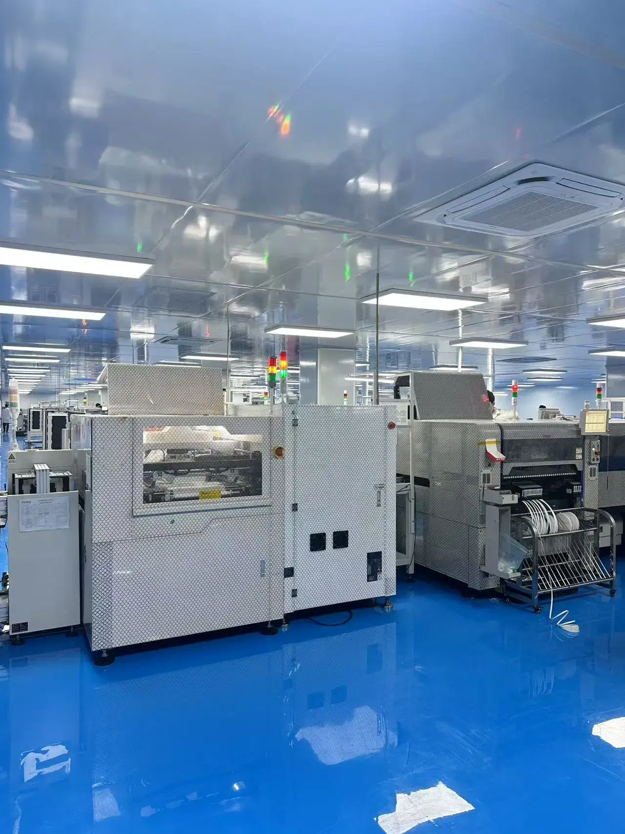
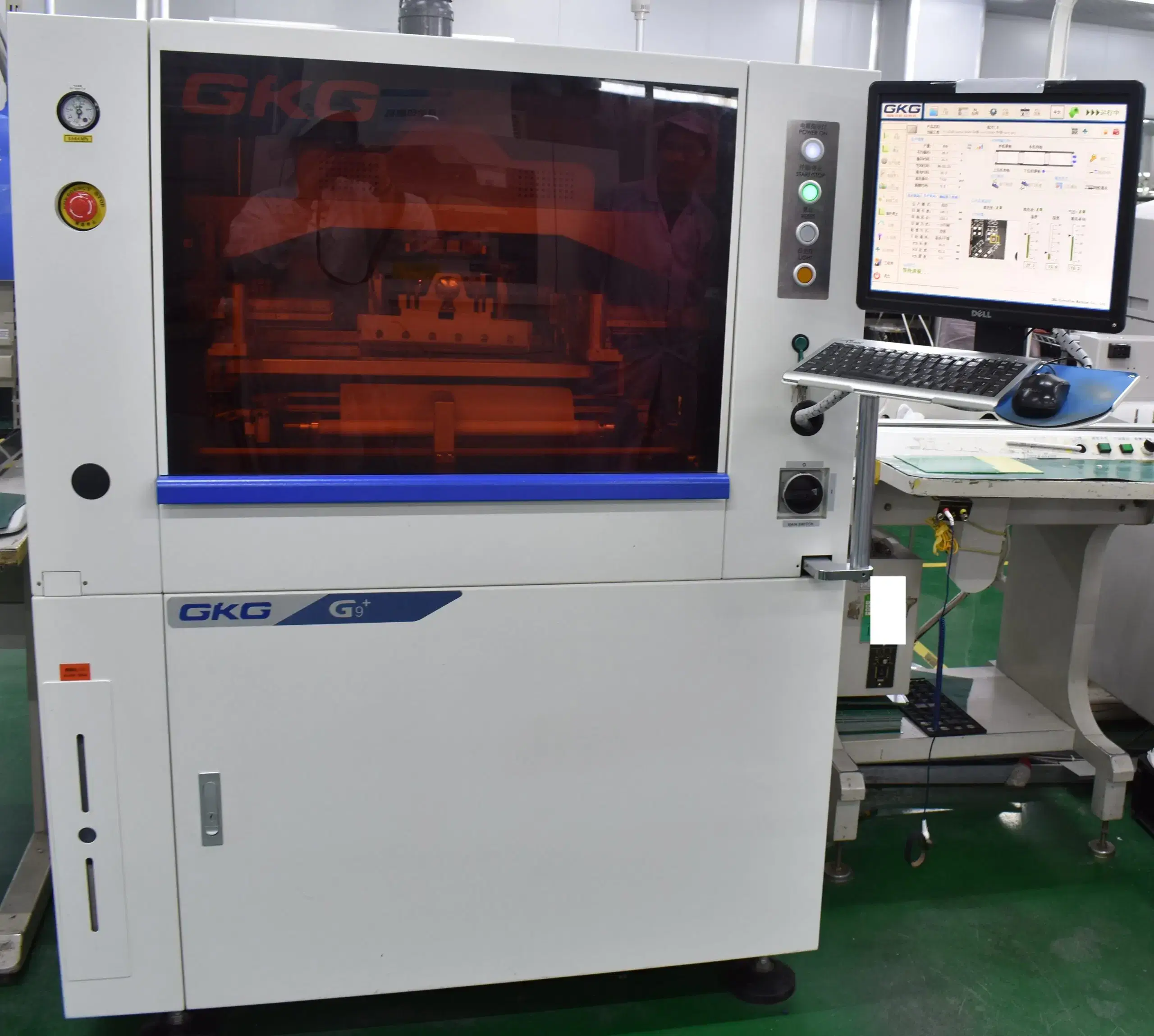
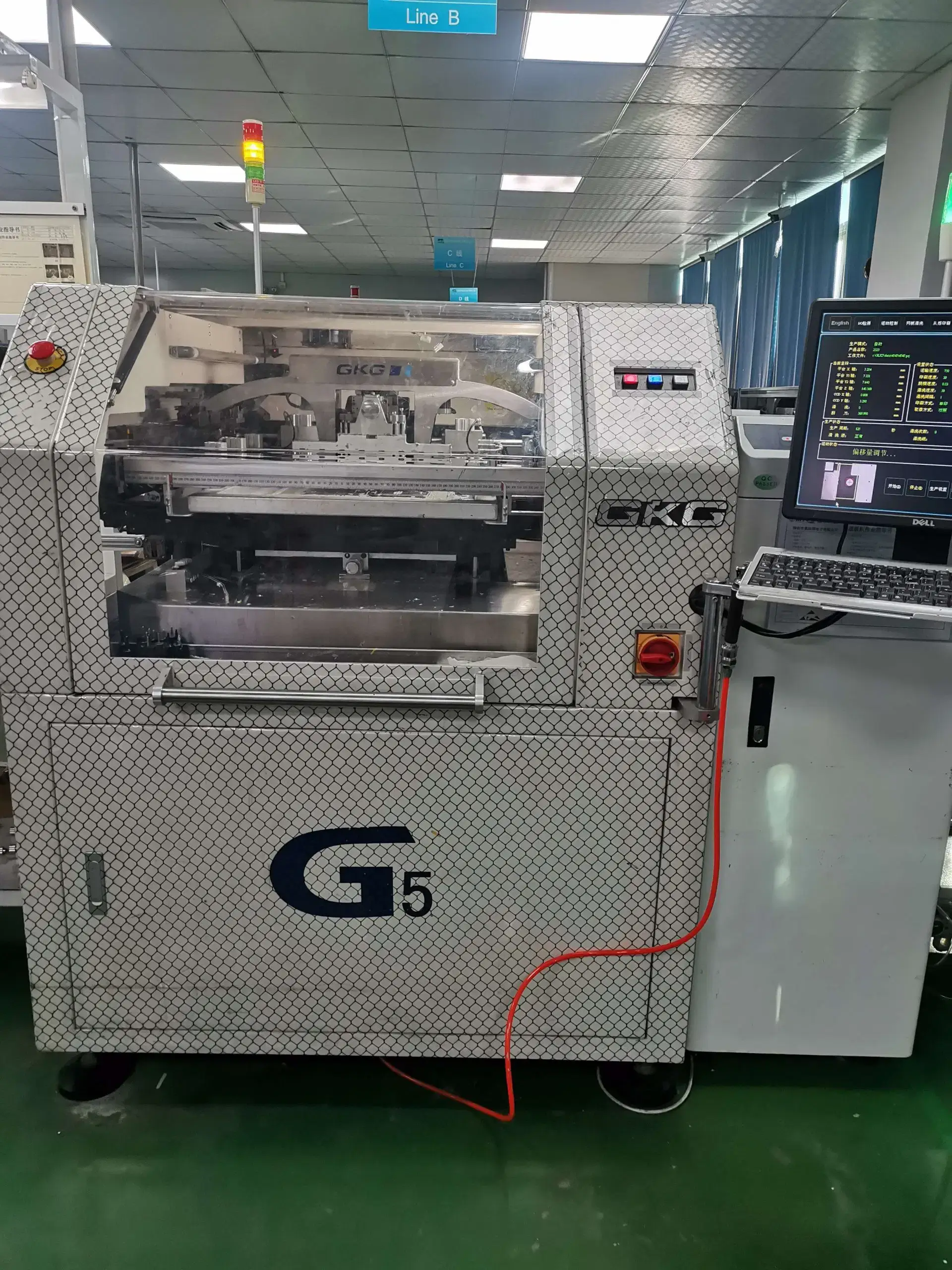
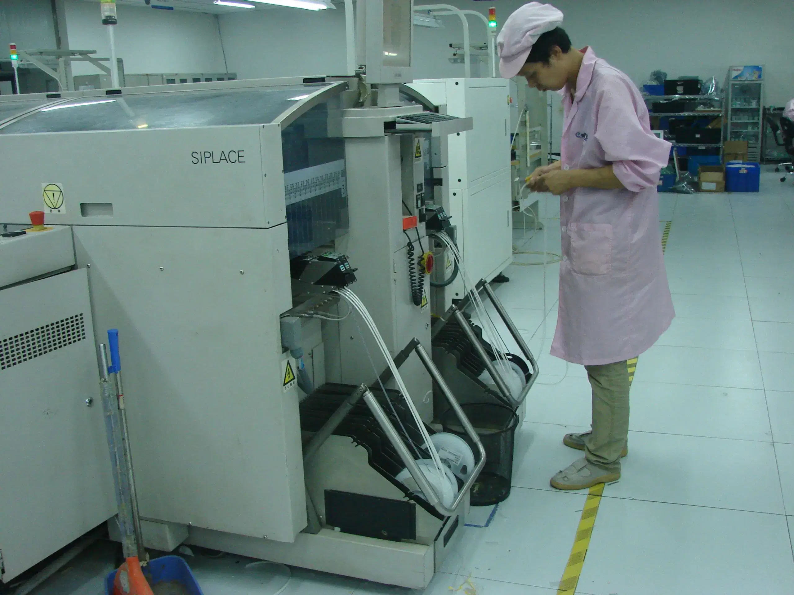
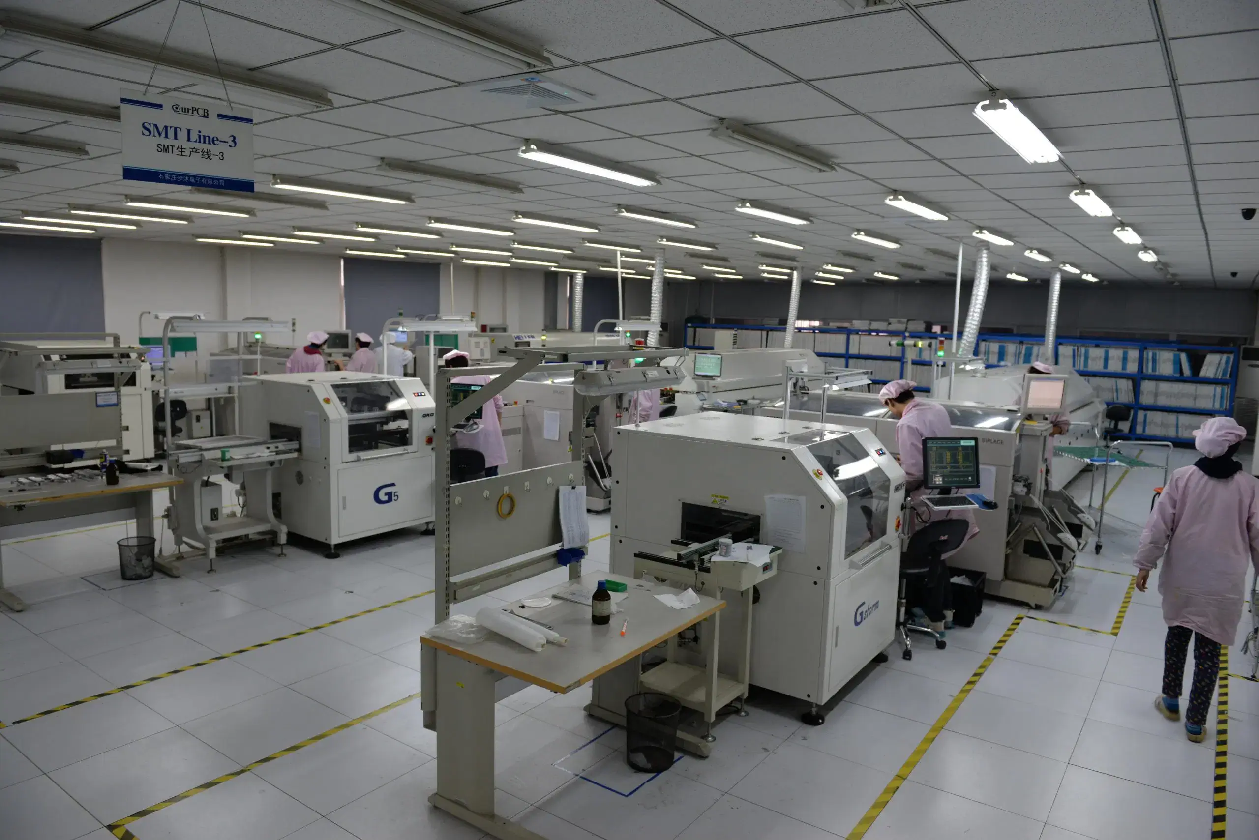
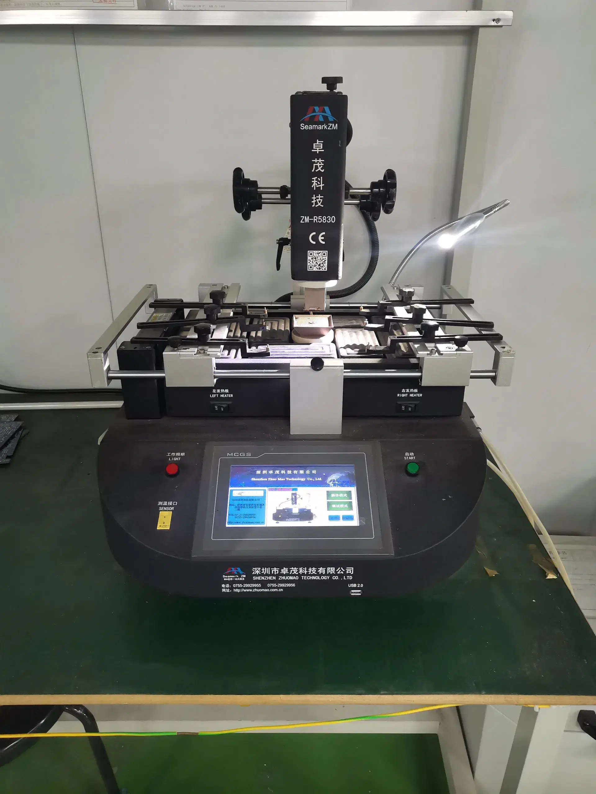
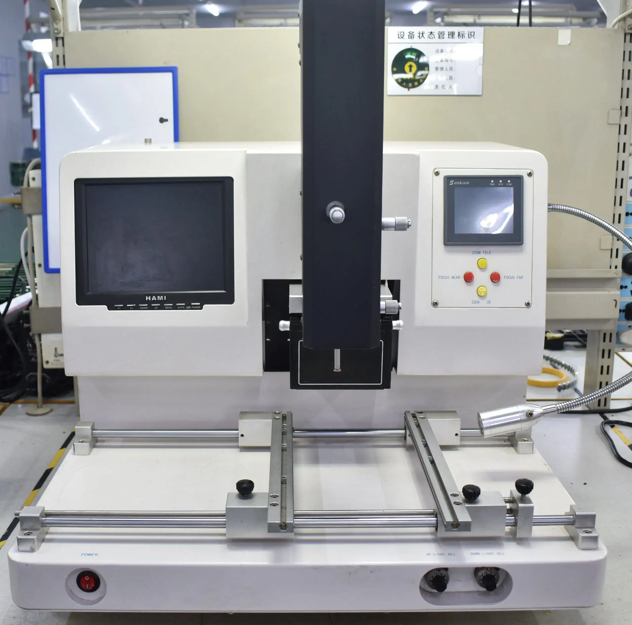
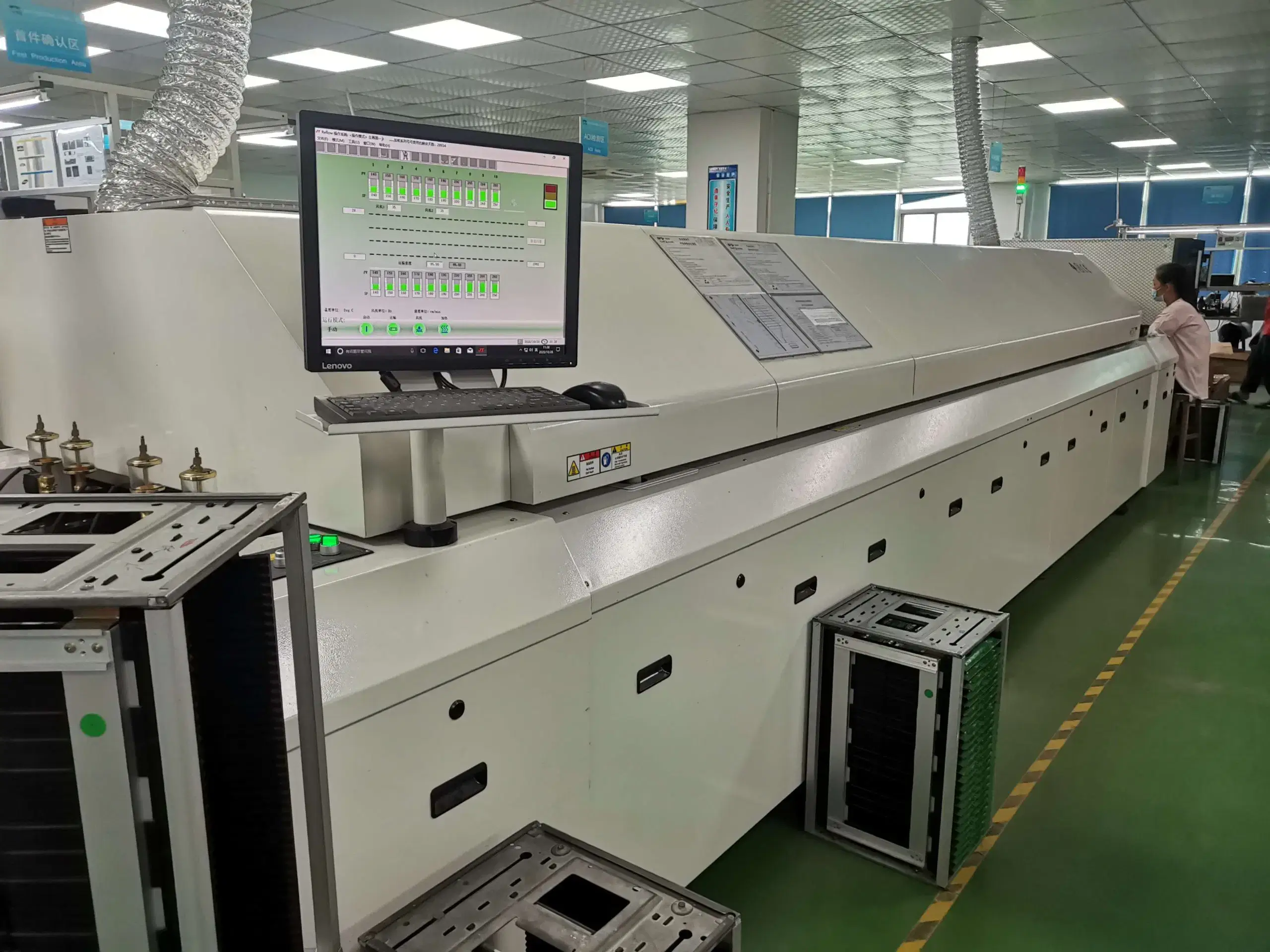
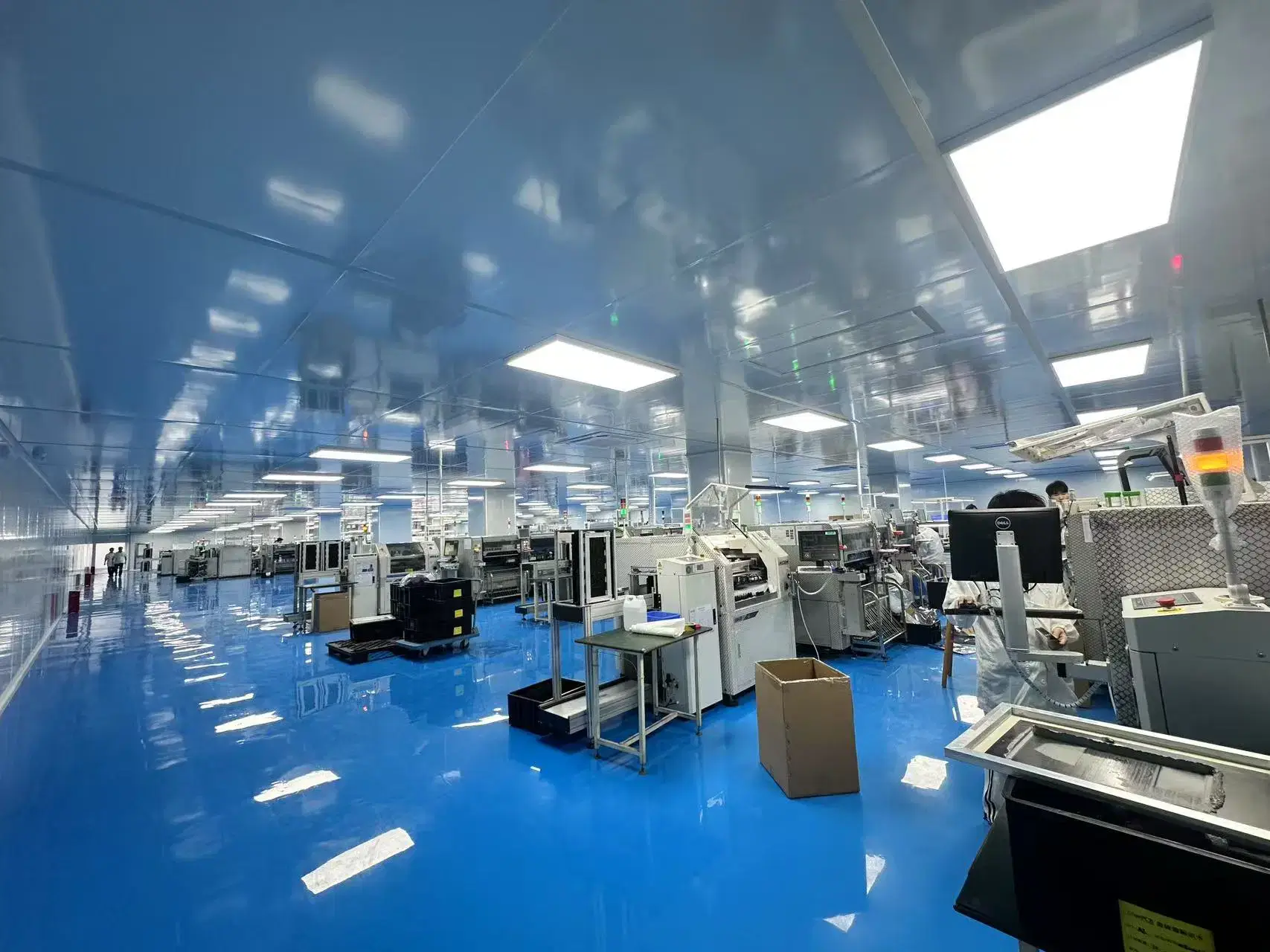
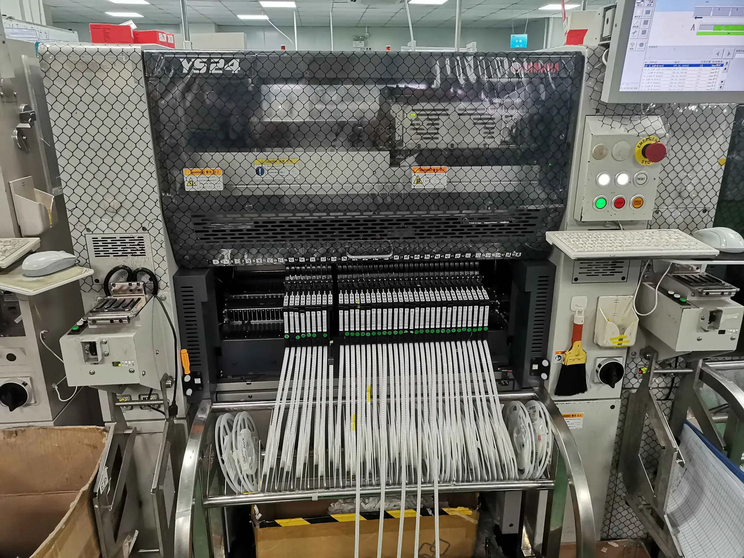
Our PCB Factory Gallery
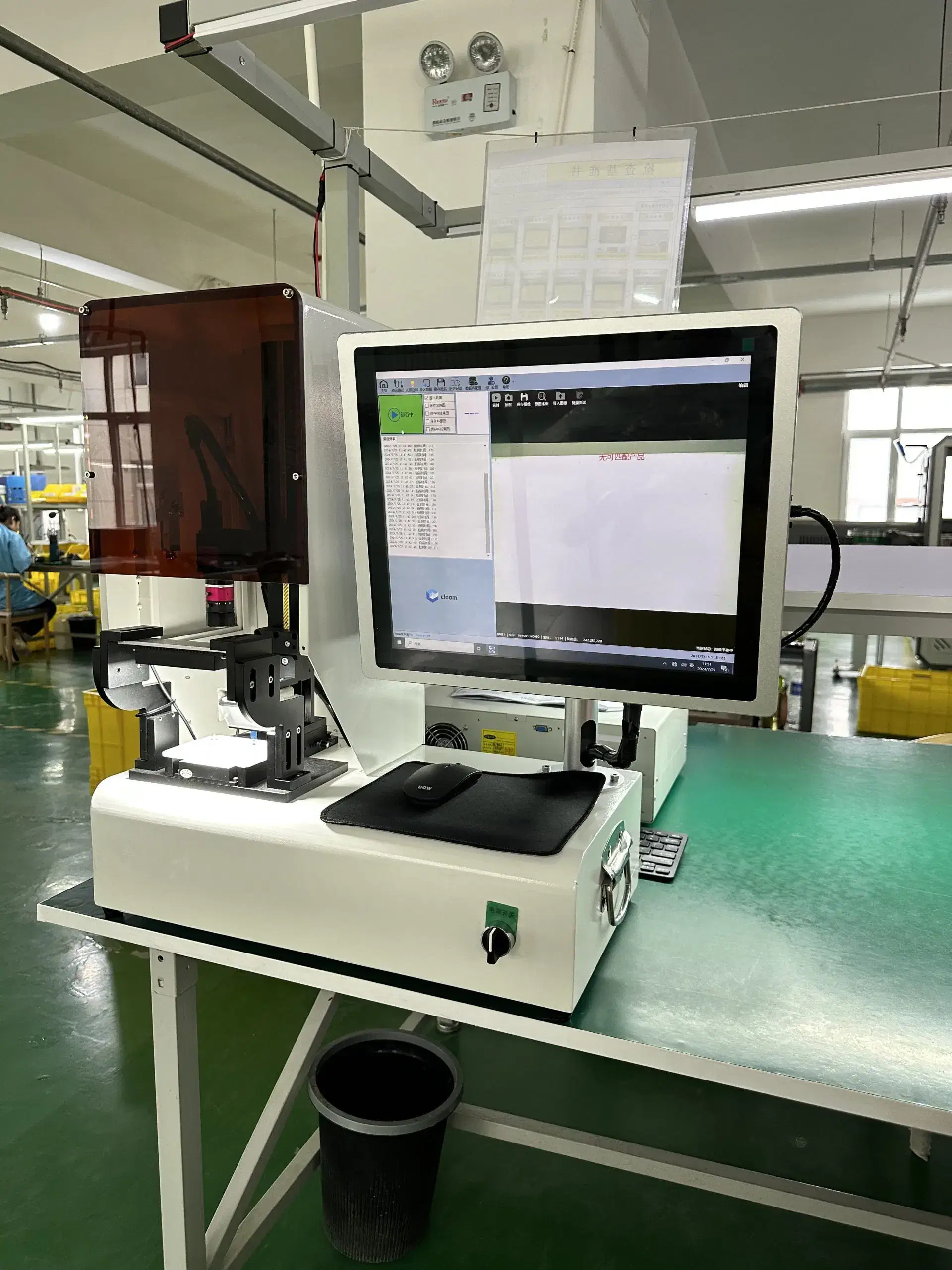
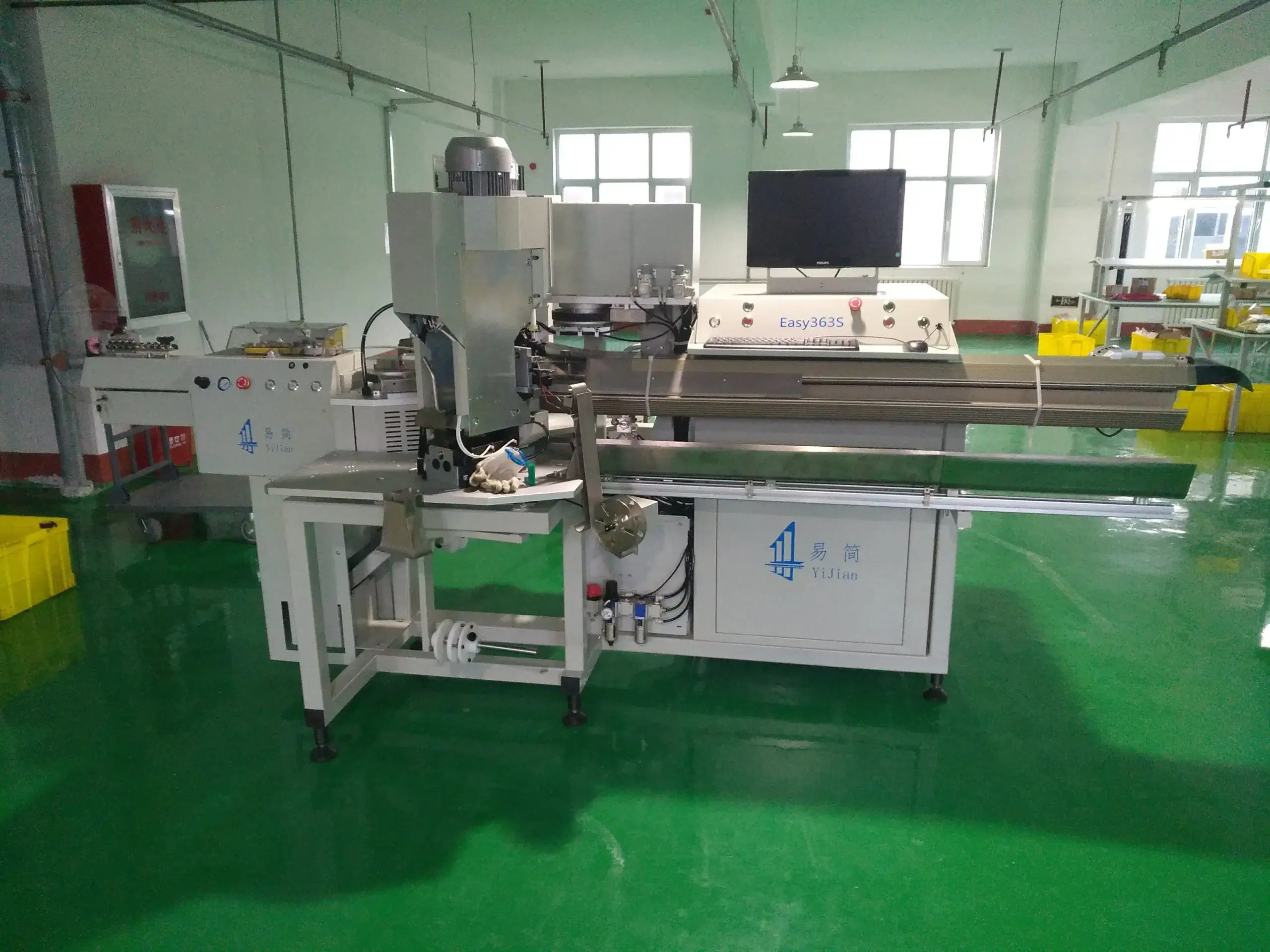
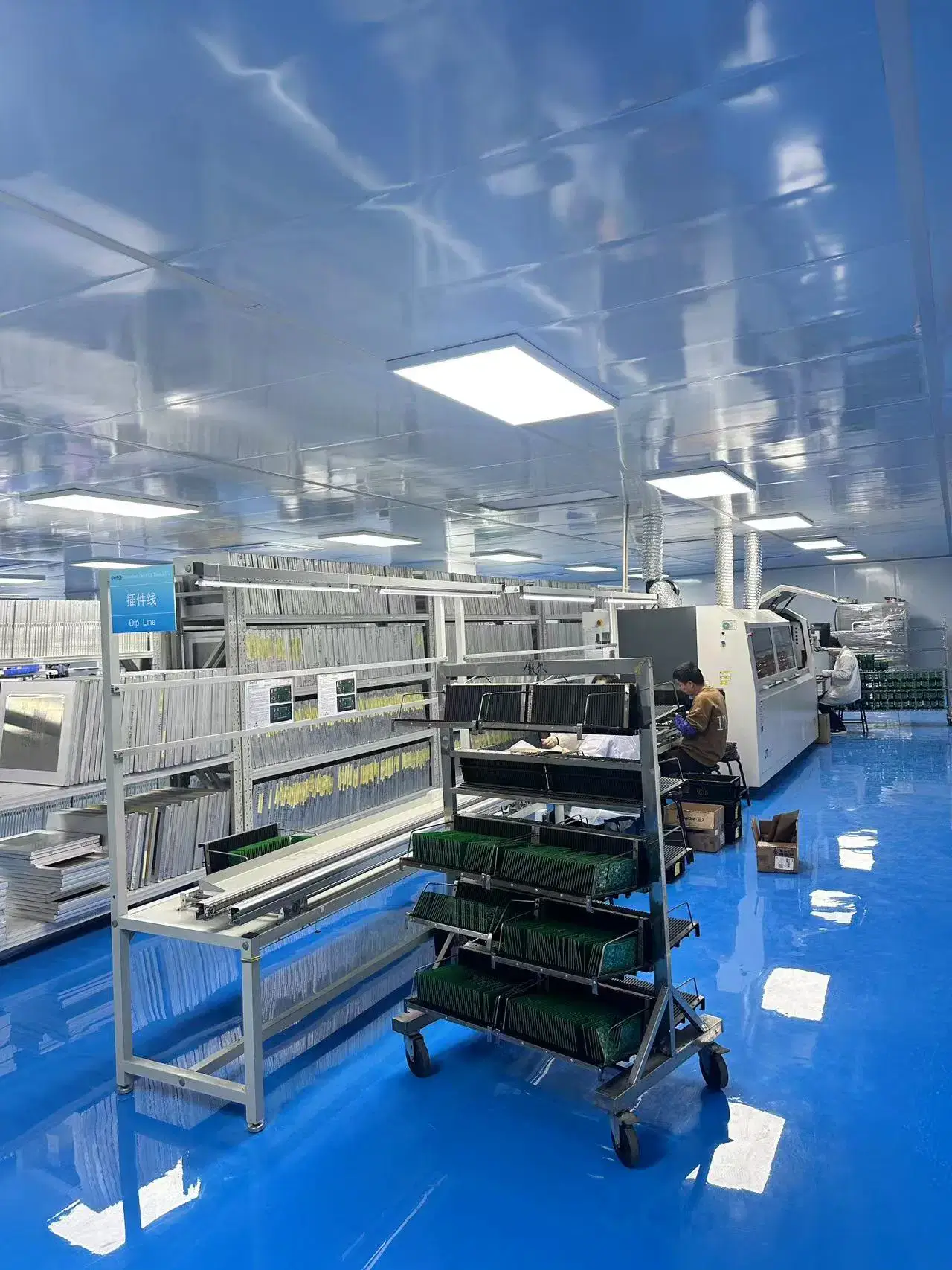
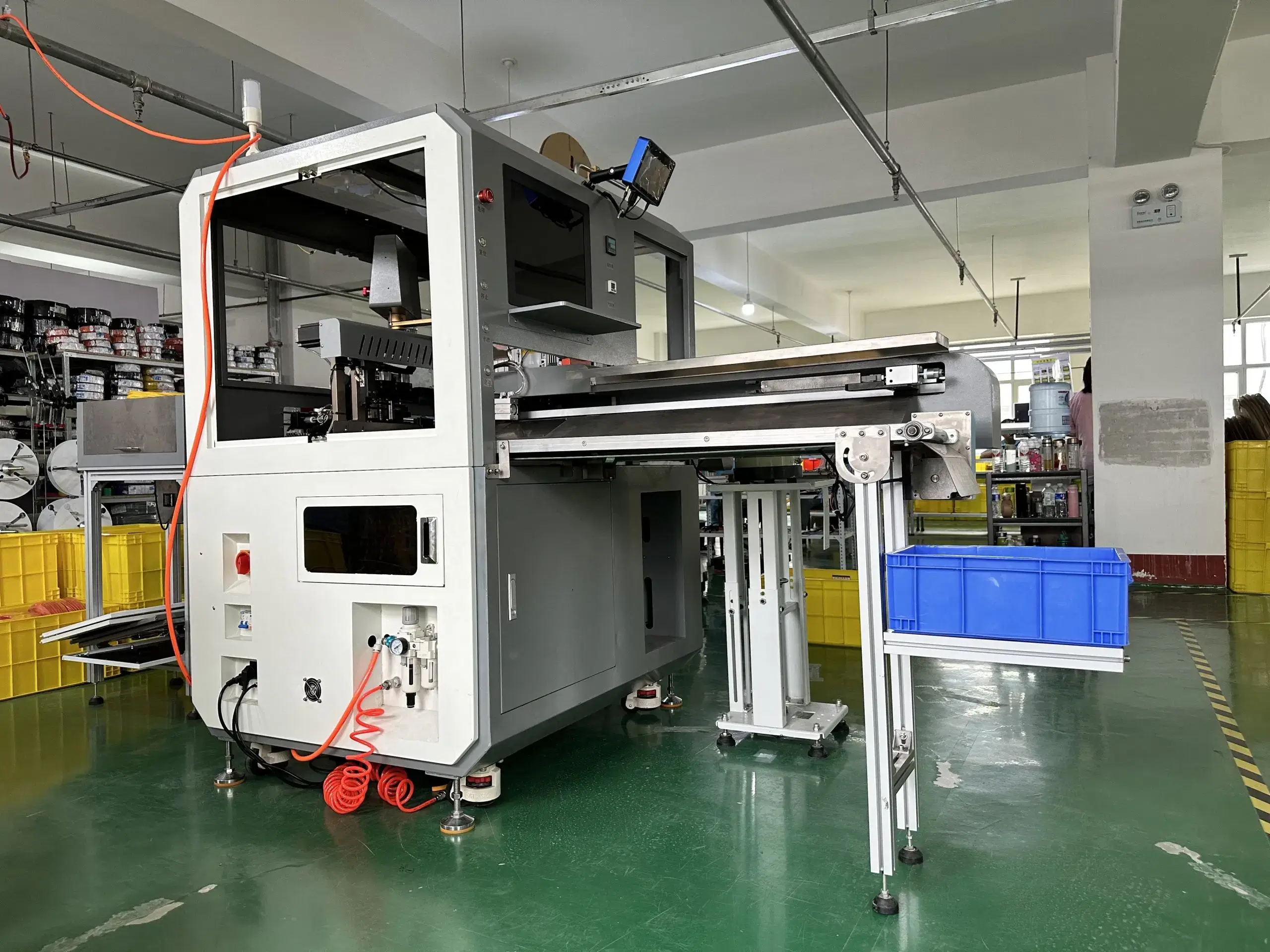
FAQ
Rogers PCB material refers to RF and microwave laminate materials used for low-loss RF and microwave applications. Rogers materials exhibit lower dielectric loss, more stable Dk and Df, and much tighter impedance behavior than traditional FR-4 does. Note, though, that the Rogers material chosen must still support the geometry and test method of the PCB.
Rogers is better than FR-4 when frequency, insertion loss, moisture behavior, impedance stability, or RF validation becomes a design factor. FR-4 can still be appropriate for lower-frequency applications, digital and power layers, or support layers in hybrid stackups.
RO4003C has process Dk 3.38 ±0.05, design Dk 3.55, and Df 0.0027 at 10 GHz. RO4350B has process Dk 3.48 ±0.05, design Dk 3.66, and Df 0.0037. RO4350B has a UL94 V-0 material rating, whereas RO4003C does not have a V-0 rating.
PTFE is used as a low-loss dielectric base for some high-frequency PCB laminate types, including RO3000 series and RT/duroid materials. It provides very low loss while requiring a different fabrication method compared with RO4000 laminates.
Yes. Hybrid stackups may contain a combination of Rogers and FR-4 materials, where Rogers materials may be used for RF portions of the stackup and FR-4 is used for lower-frequency, digital, power, or support layers.
As a relative range: FR-4 is the baseline at 1x; RO4003C averages approximately 5x-7x, RO4350B is 5x-8x, RO3003 is 8x-12x, RT5880 is 10x-15x, and RT6002 is 12x-18x, based on material costs. The overall project cost will also vary based on thickness, copper types, number of layers, holes, panelization, and testing.
77 GHz radar often requires an ultra-low-loss, stable-Dk type of PCB material; examples include RO3003, selected RT/duroid series options, and 6000-series materials. The selection should be based on the required Dk, Df, stackup, and fabrication capabilities.
Not all PCB manufacturers produce RF PCBs made from Rogers or PTFE materials. Rogers and PTFE RF PCB projects require checks for stackups, PTFE hole quality, copper plating, and impedance, all of which SUGA provides through material checks, fabrication controls, and test methods.
Yes, there is a project path that moves through prototype learning to low-volume validation and ultimately to production planning. Keep both the prototype and low-volume signals in context, as shown in the table above.