Upload BOM & Gerber
-
Mobile: +86 13312967631
-
Email: sales@sugaintl.com

HDI & Any-Layer PCB
HDI PCB and Any-Layer Interconnects in China for Fine-Pitch Designs
Fine-pitch HDI fabrication from 1+N+1 through 7+N+7 and Any-Layer, with laser microvias, via-in-pad, controlled impedance, and assembly support.
Up to 40 Layers
Up to 7+N+7
50-150 µm Laser Apertures
Down to 35/35 µm Imaging
What Are HDI PCBs and Any-Layer Structures?
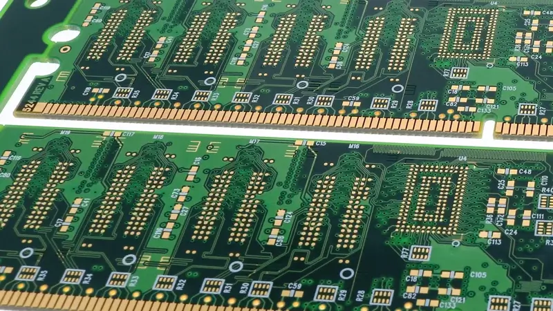
HDI PCBs make use of laser microvias, blind or buried vias, smaller capture pads, and filled via-in-pad structures to free routing channels that PTH would occupy across the full stack.
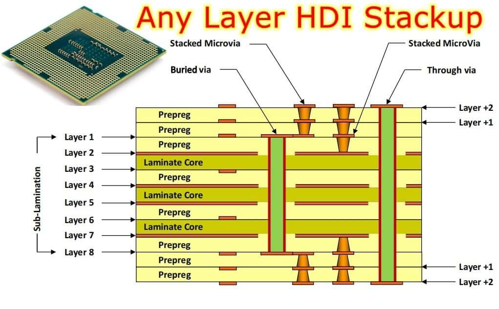
Traditional HDI limits microvia reach according to planned buildup levels. Higher-order HDI is used when the required reach extends beyond the levels available in a simpler planned stack. Any-Layer HDI forms designed adjacent-layer transitions across the required stack, so its classification depends on the connected-layer map rather than finished layer count alone.
| Architecture | Connected-layer reach | Sequential lamination cycles | Use condition | Main constraint |
|---|---|---|---|---|
| Standard multilayer PCB | PTH across the full stack; optional mechanical blind or buried structures | Conventional multilayer lamination; sub-lamination where required | Moderate I/O density with enough area for through-hole escape | Through holes consume routing and plane area on every crossed layer |
| 1+N+1 HDI | Outer layer to the first buildup layer on each side | One cycle per side around a multilayer core | Localized fine-pitch escape completes within the first buildup level | Transition depth is limited to the near-surface layer |
| 2+N+2 / 3+N+3 HDI | Two or three planned microvia levels per side | Two or three cycles per side | More escape rows or deeper planned transitions exceed 1+N+1 | Registration, fill interfaces, and planarity accumulate |
| Higher-order HDI | Structured reach through 4+N+4 to 7+N+7 | Four to seven cycles per side | Dense component fields need deeper reach without full-stack adjacent-layer freedom | Copper balance, panel movement, warpage, and interface count |
| Any-Layer HDI | Designed adjacent-layer transitions throughout the required stack | Repeated formation across the required layer pairs | Several high-I/O devices, strict thickness, or PTH blockage require broad routing freedom | Longest interface chains and the highest verification demand |
Interconnect Density Through HDI
With the increased interconnect density, it is possible to reduce PCB area, eliminate an additional routing layer, or keep reference planes continuous. For instance, with a properly executed layout, the designer may reduce an 8-layer layout to a 4-layer HDI design. This reduction is valid only when escape routing, copper distribution, impedance, current paths, and thermal reliability remain acceptable together.
How Does Any-Layer Change Interconnection?
The process of achieving routing flexibility incurs costs due to multiple lamination, laser drilling, metallization, copper filling, cap plating, and planarization. Registration errors, copper-distribution effects, dielectric variation, and surface topography are introduced in each cycle. As a result, transition count and the number of reachable layer pairs are the most important criteria for architecture selection, while layer count is less significant.
When Does Any-Layer HDI Matter?
Use the simplest HDI architecture that allows escape routing to be completed, keeps return paths and supply planes intact, and meets finished-thickness limits and the required assembly and service profile. Any-Layer is needed when limited buildup reach is not sufficient to allow the layout to be completed successfully.
Several factors must be considered, including BGA pitch and I/O count, escape-row depth, the position of high-I/O packages, transition frequency, PTH occupation, finished thickness, available dielectric spans, plane continuity, stacked-chain length, and the quality-assessment method.
Conventional HDI for Planned Transition Depth
1+N+1 should be used when outer-layer microvias are sufficient for localized fan-out while all other routes can enter the core without congestion. If additional escape rows, reference-plane changes, or deeper component fields are needed to complete escape routing, 2+N+2 or 3+N+3 should be used.
Higher-order HDI encompasses a span from 4+N+4 to 7+N+7 and enables access to deep routing regions while organizing transitions around established levels. Each additional level must unblock an existing route, protect a plane, or avoid another finished layer; otherwise, it adds processing and plated interfaces without solving a routing problem.
Any-Layer for Frequent Layer Transitions
Any-Layer is necessary when multiple dense packages require frequent transitions, when board thickness limits mechanical escape, or when through holes would fragment important signal, ground, or power channels. Mobile mainboards, optical modules, and compact computing boards reach this point when multiple fine-pitch regions compete for the same layers.
Using an insufficient stepped structure causes long detours, additional layers, narrow plane necks, and poorly controlled return-path changes. These problems can be resolved by applying Any-Layer, but the connected-layer routing map must be limited to required transitions because every stacked interface increases thermal-fatigue exposure and the verification work required.
When Any-Layer Should Be Avoided
When only one processor field creates congestion, it is usually possible to close the escape using localized 1+N+1, 2+N+2, or higher-order HDI without additional interfaces. Other methods include component rotation, pin swapping, layer reassignment, shorter transition chains, and selective use of via-in-pad.
Which Microvia Structure Matches Each HDI Stackup?
Stacked vs. Staggered Microvias
Stacked microvias are the most compact of the three. They can be positioned directly on top of one another to create a single vertical path. Stacked microvias also provide the most direct means of connecting higher-order and Any-Layer routing levels; however, thermal expansion may stress the aligned plated interfaces. Target transfer, bottom capture, copper fill, cap thickness, and thermal expansion share the same vertical interface path.
Staggered microvias require a different configuration from stacked microvias because they are offset from one level to the next. The offset consumes additional routing space but reduces the length of the direct plated-interface chain. This reduction in direct alignment provides more latitude for distributing strain between the microvia connections. Selection follows escape density, available pad field, transition depth, and the required thermal-cycling evidence.
Via-in-Pad Under Fine-Pitch BGAs
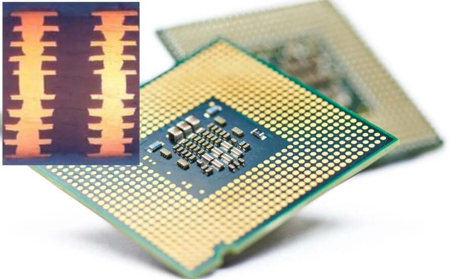
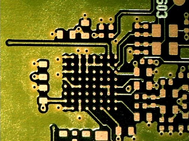
Via-in-pad microvias are located within the component land; therefore, when the cavity is filled, capped, and planarized, the surrounding routing channels remain open. A component that uses a via-in-pad microvia must have a flat land. The land must be solderable without solder wicking into the cavity. Copper fill within the via helps retain solder on the land during assembly.
A representative 100 µm microvia may use an approximately 200 µm capture pad, while component-land geometry is defined separately by the BGA pattern. Capture pad, target pad, component land, and BGA pitch are not interchangeable dimensions. A final consideration when selecting microvias is the allowable void size and cap irregularities caused by poor processing, which may affect stacked-via reliability and solder volume under the component.
Microvia Geometry and Terminology
Microvia geometries should be defined using separate values for each of the following parameters: laser top aperture (entry), target-side opening (exit), finished microvia diameter (effective), dielectric depth, capture-pad geometry, and target-pad geometry. Therefore, using only one label such as “75 µm laser via” is insufficient. The laser taper and finished plating profile can produce different top and bottom dimensions.
Most SUGA laser microvias are built to a 0.75-0.8:1 depth-to-diameter ratio, and SUGA considers a 1:1 depth-to-diameter ratio the maximum geometry capability. The ratio should provide sufficient target-pad area after considering material movement, laser positioning, and plating-process variation.
Via Reach by Layer
A blind microvia connects an outer layer to an immediately adjacent or near-surface inner layer using a thin buildup dielectric. The laser aperture size, buildup dielectric depth, target-pad size, microvia taper, and resin condition must be defined to determine whether the bottom interface of the blind microvia can be cleaned and plated continuously.
Buried vias connect internal layers of a processed buildup substructure and leave the outer layers free for routing. Buried vias may be mechanically drilled. SUGA's minimum mechanical drilling capability is 0.15 mm.
Any-Layer HDI PCB Stackup Design
Any-Layer HDI stack design begins by gathering the initial escape-row requirements, connected-layer reach, continuous reference planes, finished thickness, and maximum microvia-chain length.
| Design input | Decision to close | Interaction with the stackup | Required output |
|---|---|---|---|
| BGA pitch, pinout, and row depth | Number of escape rows and first transition layer | Determines whether dog-bone fan-out, via-in-pad, or another buildup level is needed | Marked land pattern and escape strategy |
| Connected-layer map | Exact source and destination layer for every transition | Separates stepped HDI from Any-Layer and prevents unnecessary stacked chains | Layer-to-layer via map |
| Laser aperture and dielectric span | Production ratio and target-pad capture | Controls taper, bottom cleaning, plating, and registration margin | Top aperture, target-side opening, depth, and pad dimensions |
| Stacked or staggered sequence | Vertical footprint versus interface-chain length | Changes pad-field consumption, cap planarity, and thermal-fatigue exposure | Via structure by transition |
| Signal and plane assignment | Return-path continuity and power-plane area | Prevents escape routing from cutting reference planes or narrowing high-current paths | Layer function and transition-return treatment |
| Copper and impedance | Finished copper, line/space, dielectric, and reference geometry | Affects imaging, resin flow, loss, plating balance, and finished thickness | Controlled-impedance table and copper specification |
| Material system | FR-4, high-Tg, low-loss, RCC, thin prepreg, or hybrid construction | Changes laser response, resin flow, roughness, thermal expansion, and lamination behavior | Approved material set and substitutions |
| Reliability requirement | Inspection, coupon, sampling, and stress sequence | Must match the deepest chain and the service environment rather than the easiest feature | Acceptance and qualification plan |
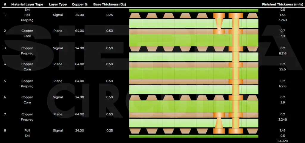
How Many Sequential Lamination Cycles Are Required?
The SLC count is established by completing the placement of all signal, power, and ground layers before beginning the buildup process and then tracing all required point-to-point layer transitions. The minimum levels required to maintain return paths while minimizing routing distance to and from components will determine the thickness consumed by repeated buildups due to the additional dielectric and copper, regardless of whether the finished product target is an ultra-thin board. The general requirements for PCBs are provided in IPC-2221C; IPC-2226A is used for the design of HDI and microvia PCBs; IPC-6012F describes the qualification and performance requirements for rigid PCBs; IPC-A-600M provides a method for interpreting visual and microsection acceptance criteria in combination with the applicable procurement class. The PCB-specific drawing and purchase specification, along with the accompanying technical documents, define the values applicable to a specific design.
Fine-Pitch BGA Escape
The BGA pitch determines how much area is available for the component lands and how wide the escape channels will be, while the number of pins and rows helps determine how many transitions will be needed to route the pins from the component to the PCB. For instance, designs may use 0.8, 0.5, 0.4, 0.35, 0.3, or 0.25 mm pitch; even when two designs have the same pitch, the number of pins in each row and the row depth will determine whether different routing structures are required.
A 0.4 mm package may use a standard fine-pitch method because it has an open center, allowing the outer rows to escape directly. Conversely, a very dense 0.35 or 0.25 mm pattern may require via-in-pad routing to accommodate a greater number of rows. An open-center pinout can increase the available escape routes and reduce the required HDI order. Each review must include the following information: pitch, I/O count, number of rows, component-land diameter, microvia capture-pad size, routing layers used, and plane continuity.
HDI PCB Design Data
The engineering package should contain the following items: Gerber or ODB++, NC drill data, an IPC-356 netlist, the proposed stackup, copper weights, controlled-impedance targets, BGA land patterns, material requirements, finished thickness, surface finish, and reliability targets. The connected-layer map and via-fill information must be clearly defined before releasing the construction.
Low-Loss Any-Layer Stackups
The channel insertion-loss limit is determined by the data rate, edge rate, channel length, and Dk and Df at the relevant test frequency of an HDI stack. Copper profile and roughness also affect the same channel. The electrical parameters associated with Any-Layer structures must coexist with thin dielectric materials, repeated lamination, microvia formation, and compatible bonding materials.
SUGA supports MEGTRON 6/7/8, I-Speed, N7000-2HT laminate, N7000-3 prepreg, and RF substrates including RO4350B, RO4003C, RO4400-series bondply, PTFE, RCC, thin prepregs, and hybrid options. RO4350B and RO4003C have different flame-rating and processing requirements, so the respective bondply or prepreg must maintain resin flow and adhesion throughout the repeated lamination process. Material selection is determined by the channel-loss target, copper profile, laser response, dielectric availability, and complete stackup construction.
Any-Layer HDI PCB Manufacturing
The manufacturing process repeats inner-layer imaging, lamination, laser drilling, cleaning, copper deposition, electroplating, filling, cap plating, and planarization to produce every required level of the stackup. Only after the entire repeated stackup has been created do final outer-layer imaging, solder mask, surface finish, electrical test, and structural verification follow.
Inner-layer imaging establishes the fine-line circuitry and registration targets used in manufacturing. Lamination controls dielectric thickness, resin flow, copper balance, and the surface presented to the next laser process. Laser drilling exposes the target pad, cleaning removes debris, and copper deposition and plating form the conductive bottom and wall profile.
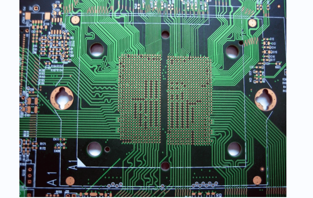
Laser-Via Formation
Laser drilling accuracy is ±15 µm. However, final capture also depends on target-pad size, dielectric movement, taper, resin response, and bottom-surface cleanliness. A clean target before copper deposition allows copper to join the target pad continuously, whereas residue or over-etch during deposition may create an interface weak enough to separate during thermal cycling.
Registration is controlled through imaging, lamination, and laser positioning. An early offset consumes capture margin in every later cycle. Target-capture margin, target transfer, and material movement are tracked before permanent plating.
Filled-Via Surface Control
The completed microvia must have a continuous metallized cavity, controlled copper fill, uniform cap plating, and a planar surface to support a component land or stacked microvia without significant local height variation.
An internal void can significantly reduce the thermal and mechanical integrity of a microvia, while thin or incomplete cap coverage can reduce the area of the next interface. Solder volume and package coplanarity may also change as a result of excessive dimple. Therefore, fill chemistry, aperture, current distribution, cap requirements, and finish determine the process sequence rather than the number of operations performed.
Sequential Lamination Control
Sequential HDI adds interconnections in stages, one layer pair at a time. Each layer pair is imaged, drilled, plated, filled, capped, and leveled after lamination. Any-Layer extends this sequence across every required adjacent-layer transition.
Registration, copper distribution, resin flow, dielectric thickness, panel movement, planarity, finished thickness, and warpage are tracked across the complete sequence.
Microvia Reliability
The interface strength of each microvia is determined by its laser response, target-surface exposure, dielectric geometry, copper adhesion, plating uniformity, fill quality, cap planarity, laminate expansion, and total connected-chain length. Each failure mechanism must be connected to an inspection method that can detect it to validate microvia reliability.
Which Laminate Supports Laser Microvias?
Standard FR-4 can support cost-sensitive HDI when its thermal and electrical characteristics match the construction. High-Tg systems provide additional thermal margin, while low-loss materials address defined channel budgets. Thin prepregs and RCC provide the dielectric spans required by small laser apertures.
Laser response depends on glass style, resin condition, dielectric thickness, copper adhesion, and target-pad exposure. Resin must fill the surrounding topography without distorting the structure or causing thickness variation. Thin 1017, 1027, and 106 prepregs and a 14-layer Shengyi TG170 structure can be supported within the applicable stackup and lamination windows.
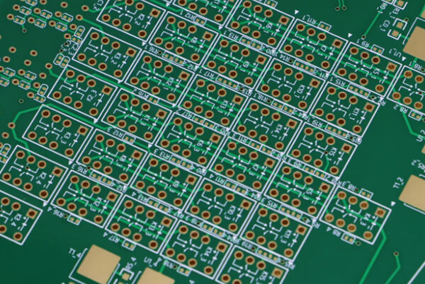
Failure Modes and Verification Methods
| Failure mode | Why basic inspection can miss it | Direct verification | Acceptance evidence |
|---|---|---|---|
| Weak bottom interface or post-reflow separation | Room-temperature electrical test can pass while the interface remains marginal | Resistance-monitored reflow or thermal cycling, followed by failure-location microsection | Resistance trend, cycle history, and pre-/post-stress interface section |
| Target-pad misregistration | AOI sees conductor images but not the buried landing interface | X-ray or µCT for alignment screening; coupon microsection for measured capture | Target capture, annular margin, taper, and bottom-contact geometry |
| Incomplete fill, internal void, or thin cap | A net can remain electrically continuous despite poor fill distribution | X-ray/µCT for void screening; destructive microsection for fill and cap profile | Void distribution, dimple, cap thickness, and land flatness |
| Stacked-chain thermal fatigue | A single static measurement does not show resistance growth across repeated heat exposure | Daisy-chain coupon with monitored reflow or interconnect stress testing | Maximum resistance change, failure cycle, and affected interface |
| CAF or insulation degradation | Continuity testing does not evaluate leakage between conductors | Insulation-resistance or CAF testing under the specified voltage, moisture, and temperature | Resistance trend, spacing, cleanliness, and material-system record |
What Each Inspection Method Proves
AOI checks for opens, shorts, and pattern defects in the conductor image.
Finished-board electrical testing checks for continuity and isolation but does not reveal internal microvia geometry. X-ray checks for gross voids, buried alignment, and fill anomalies, while µCT provides three-dimensional localization when the feature and material contrast are sufficient.
Microsections directly measure target capture, copper distribution, bottom-interface condition, fill profile, and cap geometry at the sectioned location.
Resistance-monitored reflow, thermal cycling, or interconnect stress testing challenges latent interfaces by monitoring changes in electrical resistance under stress.
CAF and Thermal Fatigue Are Different Risks
CAF develops because the combination of voltage, moisture, conductor spacing, cleanliness, and the glass-resin interface supports a conductive path. CAF control begins with conductor spacing and material selection and continues through storage, lamination, cleaning, and insulation verification. CAF can result in leakage or unstable isolation.
Thermal fatigue occurs because the thermal expansion characteristics of copper and the dielectric differ.
The strain caused by thermal fatigue depends on bottom-interface geometry, fill condition, cap thickness, plating distribution, and the length of the stacked chain. CAF requires insulation-resistance evidence, while thermal fatigue requires resistance monitoring under thermal stress and physical interface analysis.
HDI PCB & Any-Layer Capabilities
SUGA provides engineering, stackup control, advanced PCB manufacturing, verification, and assembly services for conventional, higher-order, and Any-Layer HDI PCBs in Shenzhen and the Pearl River Delta.
Capability Windows
| Parameter | Production range | Selected fine feature or limit | Production example |
|---|---|---|---|
| Via structures | Blind, buried, and through vias; laser microvias; filled and plated via-in-pad | Stacked and staggered chains for higher-order and Any-Layer interconnection | 1-, 2-, 3-step, higher-order, and Any-Layer structures |
| Layer count | Up to 32 layers | Up to 40 layers | 22-layer and 24-layer HDI structures |
| HDI buildup | 1+N+1, 2+N+2, and 3+N+3 | 4+N+4 through 7+N+7; Any-Layer | 24-layer, six-step sequential HDI |
| Finished copper | 18-70 µm | Higher-copper combinations with matched geometry | High-layer-count and low-loss HDI |
| Trace / spacing | 3.5/3.5 mil planning; 0.065/0.065 mm fine production | 2/2 mil imaging; 40/40 µm and selected 35/35 µm production | 40/40 µm mobile Any-Layer; 4/4 mil 14-layer HDI |
| Finished thickness | 0.2-6.5 mm planning range | 0.1-8.0 mm total capability range | 4-layer, 0.25 mm ultra-thin HDI |
| Finished board size | 2-20 layers up to 21 x 33 in; length up to 1000 mm | Larger or higher-layer combinations through matched panel planning | 184 x 312 mm, 14-layer HDI |
| Mechanical drilling | 0.15 mm minimum | Controlled-depth PTH 0.15 mm; NPTH 0.25 mm; mechanical aspect ratio up to 14:1 | Mixed mechanical and laser-via structures |
| Laser top aperture | 0.10 mm / 4 mil standard | 0.075-0.076 mm fine production; selected 50 µm aperture | 50 µm mobile Any-Layer aperture |
| Microvia diameter / dielectric | 0.075-0.15 mm working range | Up to 0.20 mm opening with dielectric <=0.15 mm when required | 0.10 mm blind via in a 14-layer HDI |
| Microvia aspect ratio | 0.75-0.8:1 recommended production window | 1:1 maximum geometry limit | 75-150 µm via with 200-350 µm target-pad window |
| Filled via / surface | Filled and plated via-in-pad | Filled-via diameter up to 0.45 mm; blind-via dimple <=10 µm | Filled stacked microvias and 0.10 mm blind vias |
| Minimum microvia capture pad | Approximately 0.20 mm / 8 mil | Defined with laser aperture, taper, and registration margin | Applied with 75-150 µm microvia structures and matched registration margin |
| Fine-pitch component land | Application-specific production range | 0.25 mm representative fine-pitch land | 0.25 mm pad in a 14-layer dense HDI |
| Fine-pitch component escape | 0.4 mm BGA | 0.25-0.35 mm fine-feature structures | 0.35 mm BGA mobile Any-Layer |
| Solder mask bridge | 4 mil green; 5 mil other colors at <=1 oz surface copper | 3 mil green; 4 mil black on matched constructions | Fine-line HDI structures |
| Materials | FR-4; High-Tg; high-speed and high-frequency laminates | RCC; thin PP; MEGTRON 6/7/8; I-Speed; N7000-2HT; N7000-3; RO4350B; RO4003C; RO4400-series bondply; PTFE; hybrid options | Shengyi TG170; 22-layer low-loss HDI |
| Verification | AOI and electrical continuity/isolation testing | X-ray, µCT, microsection, monitored thermal or reflow verification | Any-Layer, filled-via, and stacked-via structures |
Representative Production Structures
| Structure | Layer / buildup | Key geometry and material | Application | Manufacturing point |
|---|---|---|---|---|
| Dense consumer HDI | 14-layer HDI; blind-via construction | 184 x 312 mm; 2.0 mm; Shengyi TG170; 4/4 mil; 0.10 mm blind via; 0.25 mm pad; 90 Ω; ENIG | Dense consumer mainboard | Fine line, impedance, blind vias, material, and large format coexist in one stackup |
| Mobile Any-Layer | 10-14 layer Any-Layer | 0.35 mm BGA; 50 µm selected laser aperture; 40/40 µm line/space | Smartphone or smartwatch mainboard | High-I/O escape closes within strict area and thickness limits |
| Optical transceiver | 14-layer Any-Layer | 0.075/0.075 mm line/space; 100 Ω differential impedance (+7/-8 Ω) | Optical transceiver module | Fine-line routing and controlled differential transitions share the same module |
| Low-loss high-layer HDI | 22-layer; 4-step HDI | Rogers high-frequency material; pure-lamination stackup | RF or high-speed communication module | Repeated buildup is combined with low-loss material and controlled copper profile |
| Deep sequential HDI | 24-layer; 6-step HDI | Six sequential levels with broad planned interconnection | AI compute or communication board | Deep reach is provided without assuming that every layer pair requires Any-Layer routing |
| Ultra-thin HDI | 4-layer HDI | 0.25 mm finished thickness | Smartwatch or compact sensor board | Thin-board handling, copper balance, and warpage are controlled together |
HDI PCB Cost
HDI PCB costs depend on both the finished layer count and the number of Sequential Lamination Cycles that a board has undergone.
For example, while two 14-layer boards may have the same finished layer count, they may have significantly different cost and yield exposure profiles due to differences in their structures. A 1+12+1 build has one buildup level per side, while a 2+10+2 build repeats laser drilling, plating, filling, planarization, and registration for each additional level.
The additional cost associated with Any-Layer HDI PCBs arises because adjacent-layer freedom is required across a greater percentage of the completed stack than in a more limited adjacent-layer application.
How to Reduce Cost Without Losing Routing Function
Limit the use of via-in-pad to areas of the PCB that do not allow dog-bone routing.
Use the shortest possible connected-layer paths through the board instead of carrying every layer-to-layer transition through the entire stack. Use standard dielectric spans and stocked material systems that are appropriate for meeting specified loss limits whenever they are available.
Use 50 µm apertures or 35/35 µm imaging only in areas that require these features, rather than imposing the smallest geometry across the entire panel.
Component rotation, pin swapping, power-pin grouping, layer reassignment, staggered transitions, and localized higher-order HDI can remove an unnecessary Any-Layer conversion.
Making changes to the layer-to-layer transition maps in the early stages of a project will lead to greater cost savings than trying to negotiate the same costs after release.
Applications
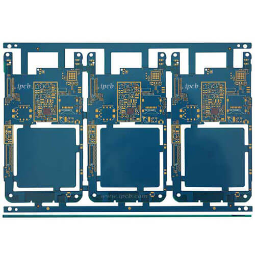
Smartphone Mainboards
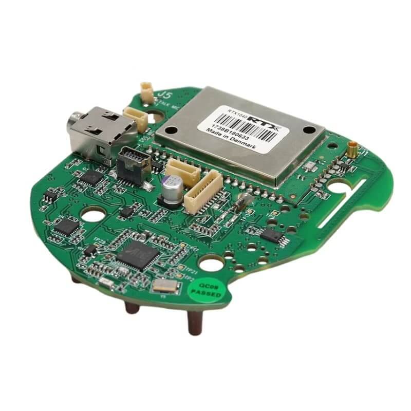
The challenge is the intersection of multiple densely packaged devices, RF keep-out zones, camera connectors, and power-plane constraints. A stepped structure is typically acceptable when all of these devices can enter the assigned layers without cutting across the processor and memory return planes. Any-Layer becomes relevant when mechanical holes would consume channels needed for repeated cross-stack transitions. Copper fill and cap planarity affect local package height, while asymmetric copper around shielded RF zones can contribute to thin-board warpage. It is common to specify via-in-pad across the processor field before evaluating whether the reflow height budget under adjacent camera or RF modules can accommodate the added cap-plating height.
Smartwatch Mainboards
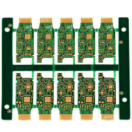
The challenge is the interaction between ultra-thin construction and asymmetric copper distribution. The typical configuration has a dense processor region paired with an open antenna or battery region on the opposite side of the board. Through holes consume both board area and thickness; however, excessively long stacked chains can experience high thermal stress after reflow and enclosure flexing. Localized HDI typically closes escape paths for the processor; Any-Layer designs should be reserved for applications with multiple competing components, such as connectors, sensors, and processors, that repeatedly require access to the same set of thin layers. In many cases, a shorter stacked chain is sufficient to close escape areas on the dense side of the board without converting the open antenna region.
Optical Transceiver Modules
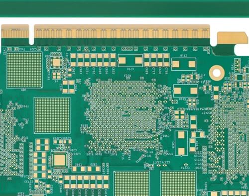
The challenge with these modules is maintaining the return path across each transition while using smaller vias; geometrically short microvias can still create a significant impedance discontinuity unless the reference plane, anti-pad, and return-via configuration is carefully controlled. Stepped HDI routing should be used when escape zones are localized to a single device; Any-Layer is commonly recommended when several fine-pitch devices require multiple cross-stack transitions without extending high-speed channel lengths. A typical mistake when validating a microvia map is to assume that the impedance target is sufficient without verifying the presence of continuous return vias adjacent to each signal transition.
AI Accelerator Boards
The conflict arises from competition between the layers used for high-density escape routing and those used to deliver large currents. Adding transitions can clear signal channels, but it is essential to avoid perforating power and ground planes. The routing stackup must retain effective copper area and support continuous return paths. In most cases, higher-order stepped HDI is preferred when dense routing is localized. Any-Layer is justified when multiple processor or memory fields require broad cross-stack freedom and the saved routing layers offset the additional interface count. Verify whether additional stacked interfaces increase decoupling-loop inductance around processors.
Automotive Radar Modules
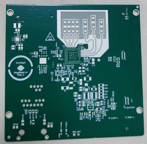
This is challenging because RF geometry and dense digital HDI must coexist in a compact mixed-material stack. Layer movement and resin flow during repeated lamination can change the dielectric thickness of RF materials and also modify microvia capture.
Microvia fences are not equivalent to BGA escape chains and therefore must be specified separately. Qualification must also consider bottom-interface resistance, insulation stability, and controlled impedance after thermal exposure rather than relying solely on a visual acceptance method.
Treating the RF and digital areas of the module as a single lamination schedule frequently results in dielectric-thickness drift beneath the antenna structure.
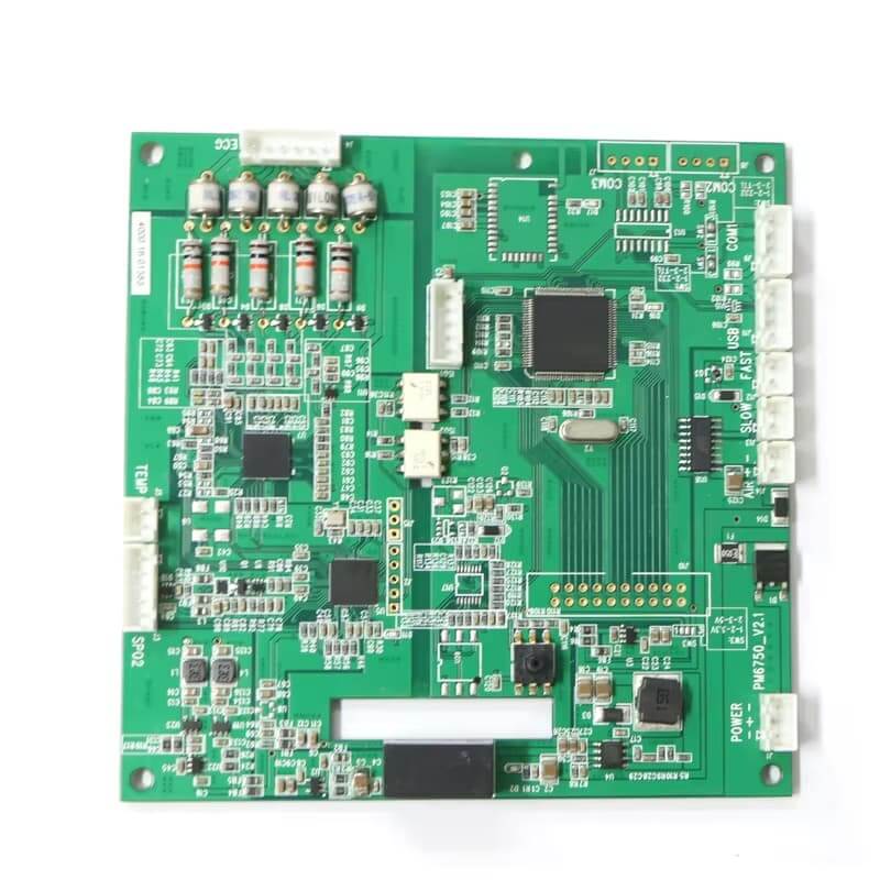
Patient Monitoring Boards
The primary conflict exists between board density and electrical isolation; board densification must not compromise creepage, clearance, isolation slots, or the return paths of sensitive analog signals.
Local routing is enabled by HDI near processors and miniature connectors, and selective layer transitions are used to keep noisy digital currents away from the measurement front end. Cleanliness and insulation-resistance evidence address leakage, while monitored thermal stress and microsectioning identify intermittent opens in filled or stacked interfaces. Typical design mistakes include applying conventional fine-pitch spacing guidelines to creepage and clearance areas, which HDI density reduction must not override.
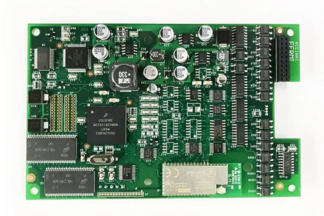
Avionics Control Modules
An additional risk results from the combined stresses of assembly reflow, wide operating temperatures, vibration, and long service life. A connection that originally passed continuity can develop resistance growth at the deepest stacked interface. Higher-order HDI or Any-Layer technologies can shorten critical interconnects, but the chain length, material expansion, copper distribution, and coupon design must match the environmental profile. Post-stress microsectioning is used to locate the interface identified through electrical monitoring; it is not the sole reliability screen. Treating a room-temperature continuity test as final qualification without thermal cycling combined with vibration testing is a common source of field failures.
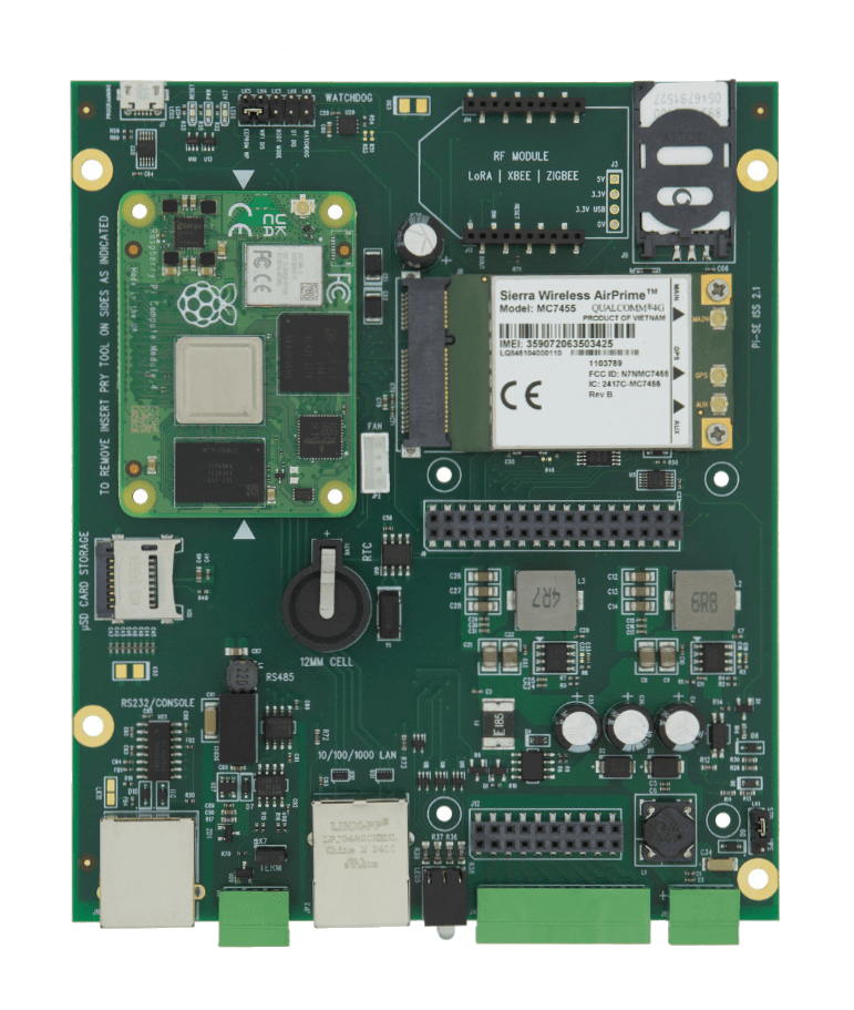
Compact Processor Modules for Industrial Gateways
Most industrial gateway carrier boards do not require full Any-Layer construction. Density is generally concentrated in the compact processor module containing the CPU, memory, wireless interfaces, and high-speed I/O connections, while isolated I/O and power are typically located in lower-density sections of the board. A localized 1+N+1, 2+N+2, or higher-order HDI configuration can clear the processor footprint without requiring repeated processing of the entire carrier. Any-Layer should be used only when multiple dense devices or board-to-board connectors require repeated transitions through the module. Separating the module from the carrier enables a lower-cost overall board design.
Our PCBA Production Lines
















FAQ
Bottom cracking in plated microvias is typically caused by a weak interface between the target pad and the microvia due to a combination of target exposure, microvia taper, plating distribution, fill condition, cap geometry, and thermal expansion. Poor contact between the microvia and the target pad can allow a continuity test to pass at room temperature but become unreliable when exposed to heat. Resistance-monitored reflow or thermal cycling tests will show an electrical change. After microsectioning the microvia, the separation, thin copper, or poor bottom capture can be identified.
Any-Layer HDI and ELIC have substantial commercial overlap. When designing Any-Layer HDI or ELIC, the fabrication drawing should contain the actual adjacent-layer transitions and complete stackup of the finished board, as well as the fill and cap sequence and lamination order, rather than referring only to the label.
No. However, stacked microvias provide a direct vertical path while preserving routing space. Stacked microvias can be used with staggered microvias or mechanically drilled buried structures based on the available pad space, transition length, and thermal reliability of the stack. The connected-layer map determines the structure.
To review Any-Layer HDI, provide Gerber or ODB++, NC drill data, an IPC-356 netlist, the target stackup, copper requirements, controlled-impedance targets, BGA land patterns, material requirements, finished board thickness, surface finish, and reliability criteria, such as the maximum allowable void size. Each blind, buried, stacked, or staggered transition should clearly identify both its source and destination layers in the data set.
SUGA supports higher-order structures through 7+N+7 and Any-Layer interconnection. The permitted stack also depends on dielectric depth, aperture size, target-pad capture area, registration margins, copper fill, cap planarity, material system, and the required thermal evidence. Longer microvia chains should undergo monitored stress testing and interface-specific microsectioning before being approved for high-reliability applications.