Upload BOM & Gerber
-
Mobile: +86 13312967631
-
Email: sales@sugaintl.com

Robot PCB Assembly Service
Choose The Right Assembly Process For Robot Circuit Boards
We are a China wholesale intelligent robot PCB manufacturer, coordinating controller, sensor, power, communication, and safety PCBAs through fabrication, assembly, inspection, functional testing, and repeat production.
AOI + X-ray + ICT + FCT
10 units to several thousand
What Is Robot PCB Assembly?
A robot PCBA is an electronic assembly on a PCB made for a robotic subsystem. It can perform a defined board function and allows programming, testing, and verification at board level. Acceptance at the board level does not indicate complete robot acceptance.
A robotic PCB provides the electrical interconnect of the fabricated PCB, and a robotic PCBA adds the components and solder joints needed to perform the defined function.
Board Acceptance Limit
Acceptance at the board level may be based upon inspection records, testing and programming test data, ICT data, FCT limits, and traceability to the PCBA revision. This evidence supports release of the robot PCBA, but it does not recreate the entire robot operation: cable routing, actuator installation, mechanical alignment, housing integration, calibration, and complete system operation, as defined by robotics. Board acceptance limitations should be explicit.
Assembly verifies the identity, orientation, location, solder quality, programming status, and electrical characteristics of the components, and it allows testing.
The robot assembly may pass a fixture test but may also reveal an interface issue once connected to the motors, sensors, harnesses, and mechanics of the robot. The board approval indicates that the finished PCBA matches the specified design, while system validation ensures that the robotic system has been integrated into the final product.

Robot PCBA Board Functions by System Role
Robot PCBAs are classified according to the role the PCBA plays in the system: control, power, sensing, communication, safety I/O, and user operation.
Because of the complexity of many robotic systems, there can be many PCBA types present within a single system. Maintaining assembly control and documenting test results based on each individual board’s interfaces and potential failure consequences is important.
Deterministic Motion Control Boards
They include an MCU, SoC, FPGA, or CPU processing device in conjunction with connected devices, safety logic, memory, real-time buses, and motor control commands. Robot controller PCBs may be found in complex AI robotic systems. These PCBs coordinate movement using AI-based control logic, whereas a typical controller PCB may be a stand-alone compute board.
When assessing the quality of any robot board that controls movement, there are a wide range of factors that can cause movement to become unstable regardless of whether the assembly is visually acceptable. Examples include timing errors, noise on the rail, firmware behavior, and mismatched bus speeds. Therefore, power-up behavior, programming identity, timing-dependent inputs and outputs, and communication with designated interfaces will all provide supporting evidence for a robot board’s functionality.
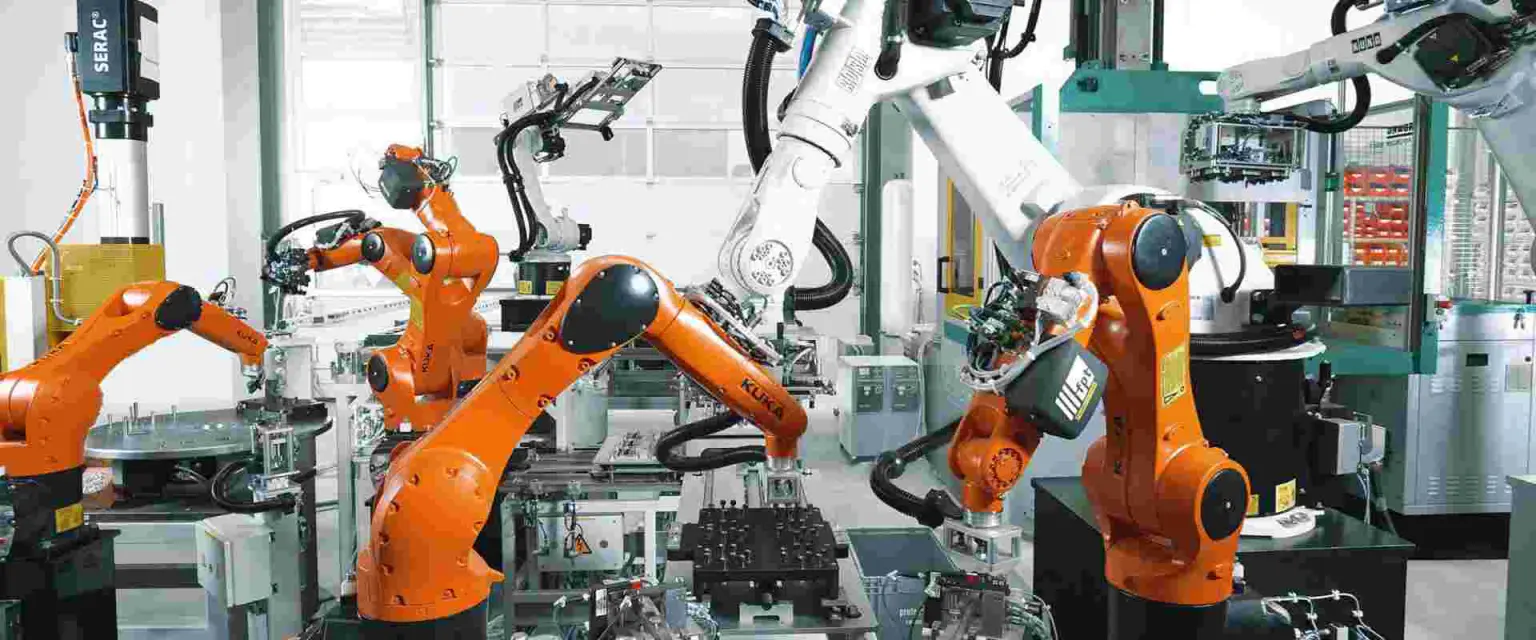
Robot Power Boards
Power boards provide DC input to the motors and batteries of a robot. They carry both voltage and current through a series of components and connect to the motors or batteries of the robot via connectors or leads. Copper traces, thermal concentration, soldering on connector pins, and load response are much more critical than simple continuity. Evidence should show that a robot battery module or AI robot power PCB module’s current path and protection match those of the robot motors or batteries.
Robot Sensor Boards
Robot sensor PCBs connect the robot’s sensors, such as touch and vision sensors, to an AFE or to local processing. Some of this processing is performed before communication with the controller, and some is performed synchronously, with reference to the AFE clock. Low-noise local power and ground will maintain small signals prior to being fused with the signals from other sensors or before local processing is used.
Although an AI robotic sensor module PCB may pass inspection, if the sensor’s calibration, timing, or response is incorrect, it will usually produce abnormal output, such as unstable readings. All functional evidence should be documented following the entire sensing chain.
Industrial Communication Boards
Robot motor drives are connected via PCB links, such as EtherCAT, to EtherCAT PHYs. PCB designs for robot navigation and WiFi wireless communication also include their respective channels. If a communication break occurs along the return path, or if there is an impedance mismatch, EMI issue, or clocking error, a failed communication link may occur. The communication protocol and physical interface should be tested after assembly, and the results should be documented.
Safety Interface Boards
Safety I/O boards provide the interface for user emergency stops, as well as an interface for user communication requests through a teach pendant or HMI interface and feedback to the user based on performed commands. Although both safety I/O and teach pendant or HMI interfaces use connectors and digital I/O, they have different functional consequences when they fail.
Safety I/O failures will have different consequences than a properly mounted HMI when the HMI connector comes loose or has an intermittent state transition. The polarity of connectors, connector retention, state transitions, and traceable functional results for these two types of boards will merit specific deterministic checks.
Custom Robot PCB Manufacturing
Custom robot PCBA and custom PCB for robotics programs should be developed following the same process discipline. Therefore, process numbers alone do not provide sufficient evidence that a product will meet the intended use and application requirements. Each process must connect the capability to a robot function so the result can be checked.
| Board condition | Capability data | Robot function | Manufacturing control | Acceptance evidence |
|---|---|---|---|---|
| Fine-pitch packages | 0.20 mm / 0.25 mm BGA ball diameter where specified; 01005 / 0201; 0.25 mm QFP pitch; ±30 µm placement; ±25 µm solder paste alignment where verified | Dense controller, vision, sensor fusion, AI compute, compact joint electronics | Stencil design, moisture control, feeder setup, placement program, reflow profile | SPI, AOI, package-specific X-ray, placement record, first-article result |
| High-current copper | standard 1–2 oz copper; up to 20 oz copper where design requires it | Motor drive, battery path, power distribution, high-current connector boards | Copper balance, thermal profile, via/current path review, connector soldering | Temperature-rise evidence, functional-load result, solder-joint inspection |
| Multilayer / HDI interconnect | 0.15 mm finished drill; 12:1 aspect ratio; controlled stack-up; 12 layers are not a final capability cap | Controller, industrial communication, sensor processing, compact main control board | Stack-up review, drilling, plating, lamination, impedance control | Cross-section, continuity, impedance evidence, board identity record |
| Rigid-flex / flex structure | 0.2–6.0 mm thickness; bend radius, flex stack-up, copper weight, stiffener position, and cycle requirement must be defined | Moving joints, grippers, compact sensor modules, cobot arms | Bend-zone DFM, panel support, solder-heat control near flex transition, connector reduction | Bend-cycle test when required, continuity before/after cycling, visual inspection at transition area |
| Flatness / board stability | ≤0.7% warp/twist | Dense BGA boards, rigid-flex panels, multi-board assemblies | Panel design, thermal balance, lamination control, post-reflow handling | Flatness check, post-reflow evidence, X-ray escalation when hidden joints are affected |
| Controlled impedance / RF laminate | ±5% impedance control; Rogers / RF laminate where specified | EtherCAT, industrial Ethernet, wireless modules, high-speed sensor links | Stack-up, trace geometry, material control, return path, connector transition | Impedance coupon/TDR, communication-loop evidence, revision-matched record |
| Thermal or high-power substrate | metal-core PCB where thermal path requires it | Motor power, LED/vision lighting, battery charging, power conversion | Material selection, thermal interface, copper balance, solder profile | Thermal evidence, functional load, visual/AOI inspection |
| Contact / wear surface | Hard Gold where mating cycle or contact reliability requires it | Edge contacts, programming pads, high-use connector interfaces | Plating spec, surface finish selection, connector review | Surface finish record, contact inspection, continuity evidence |
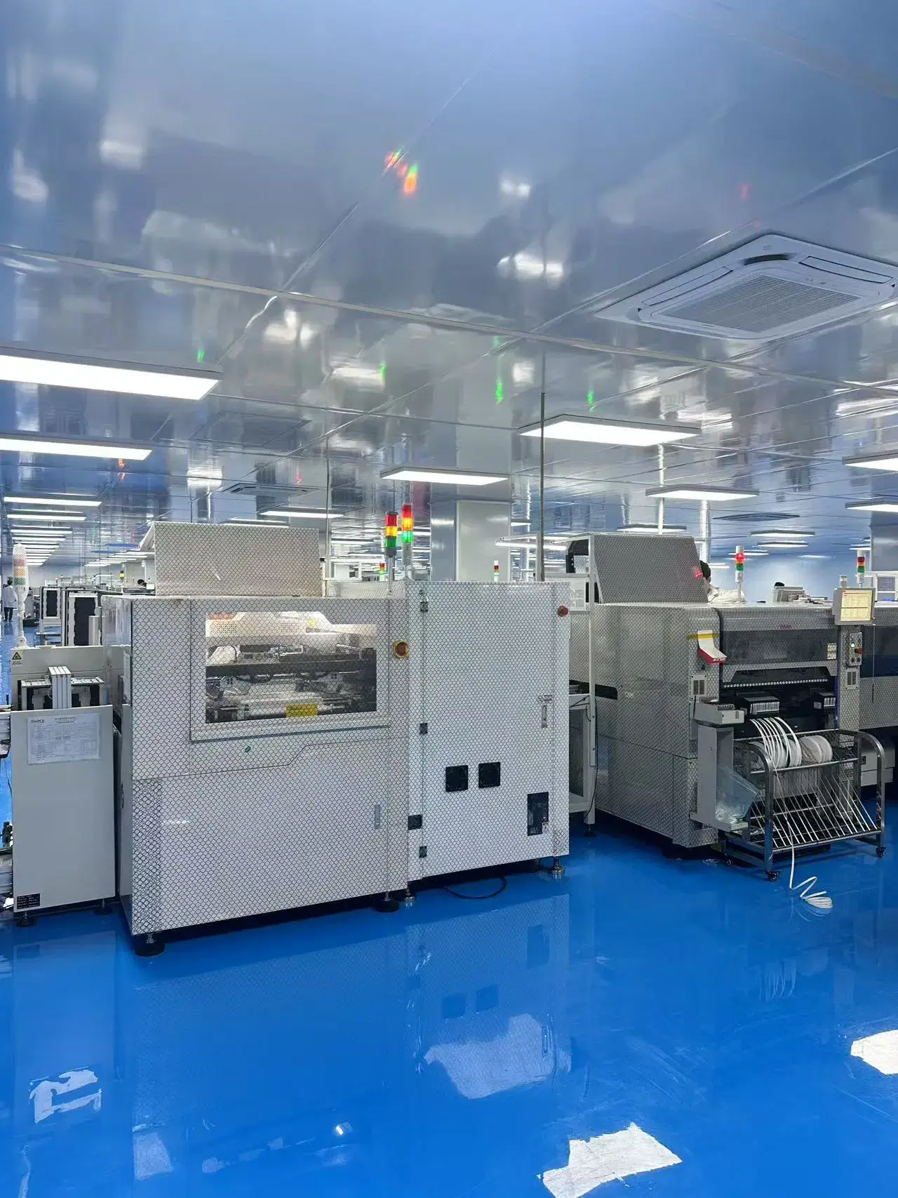
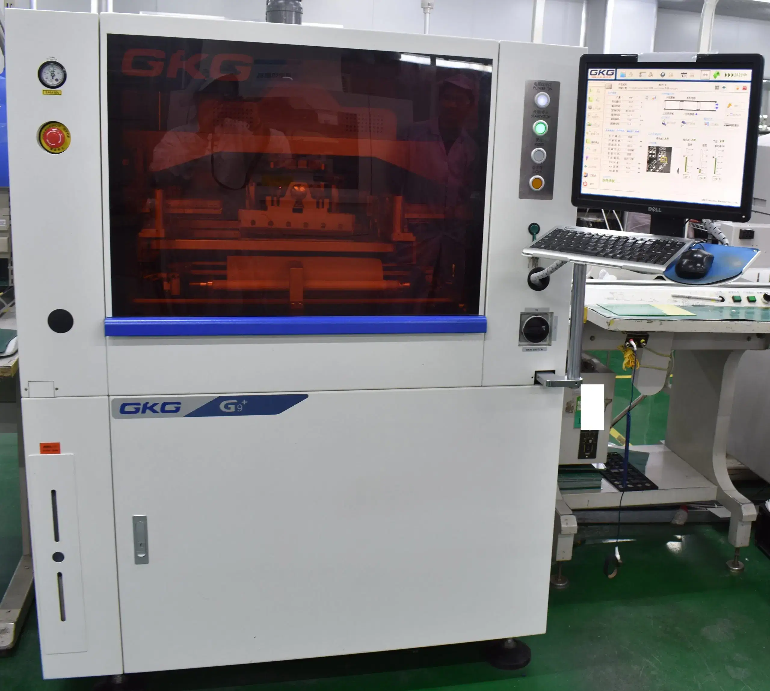
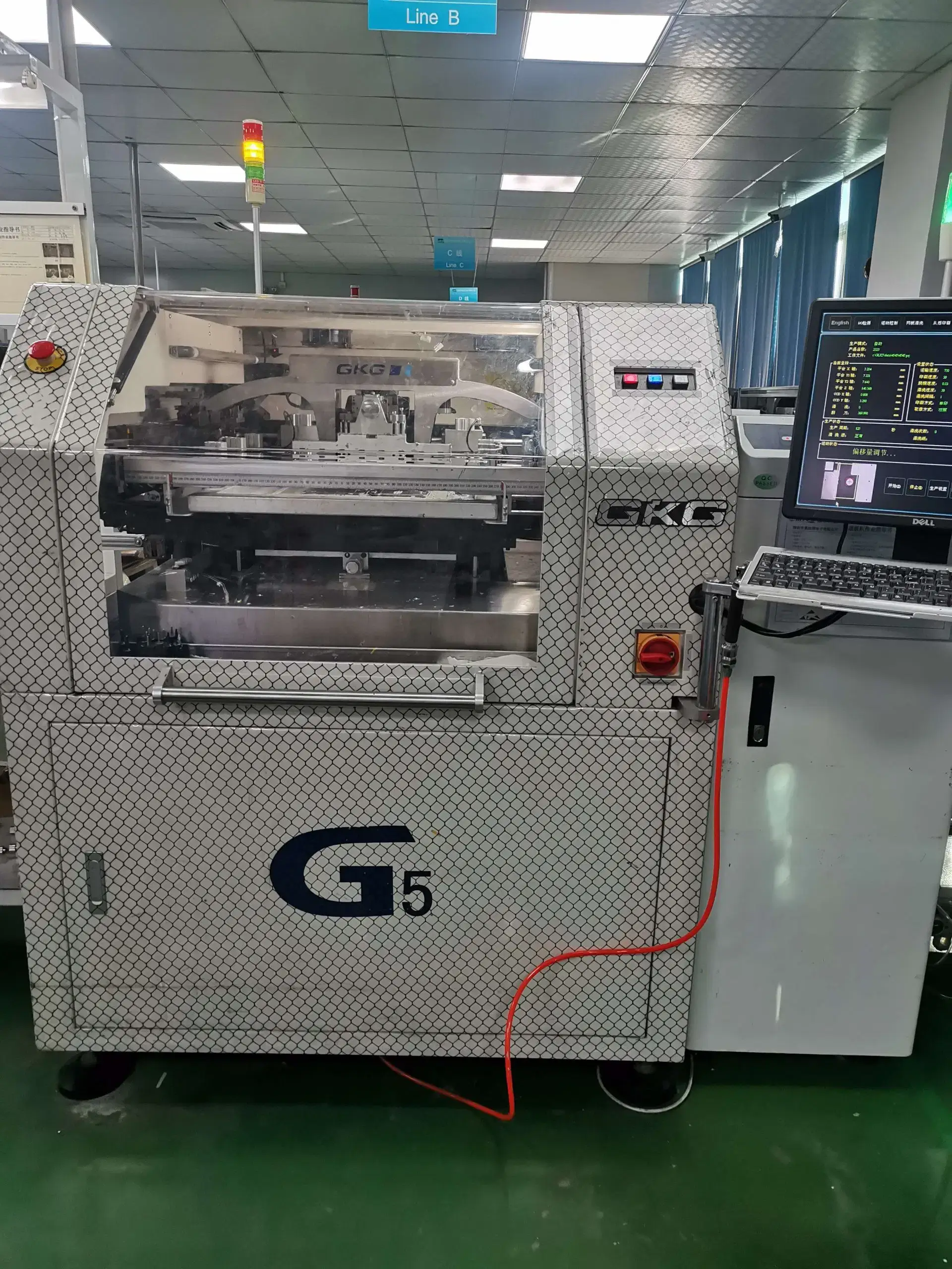
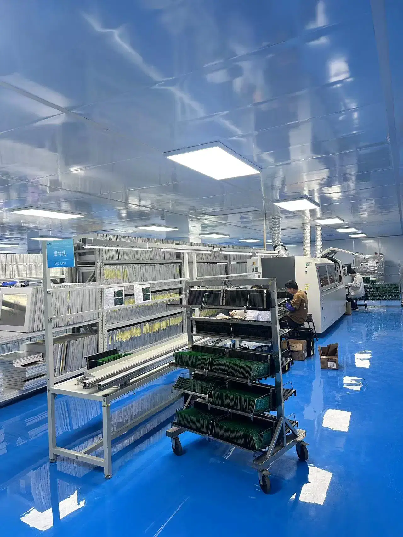
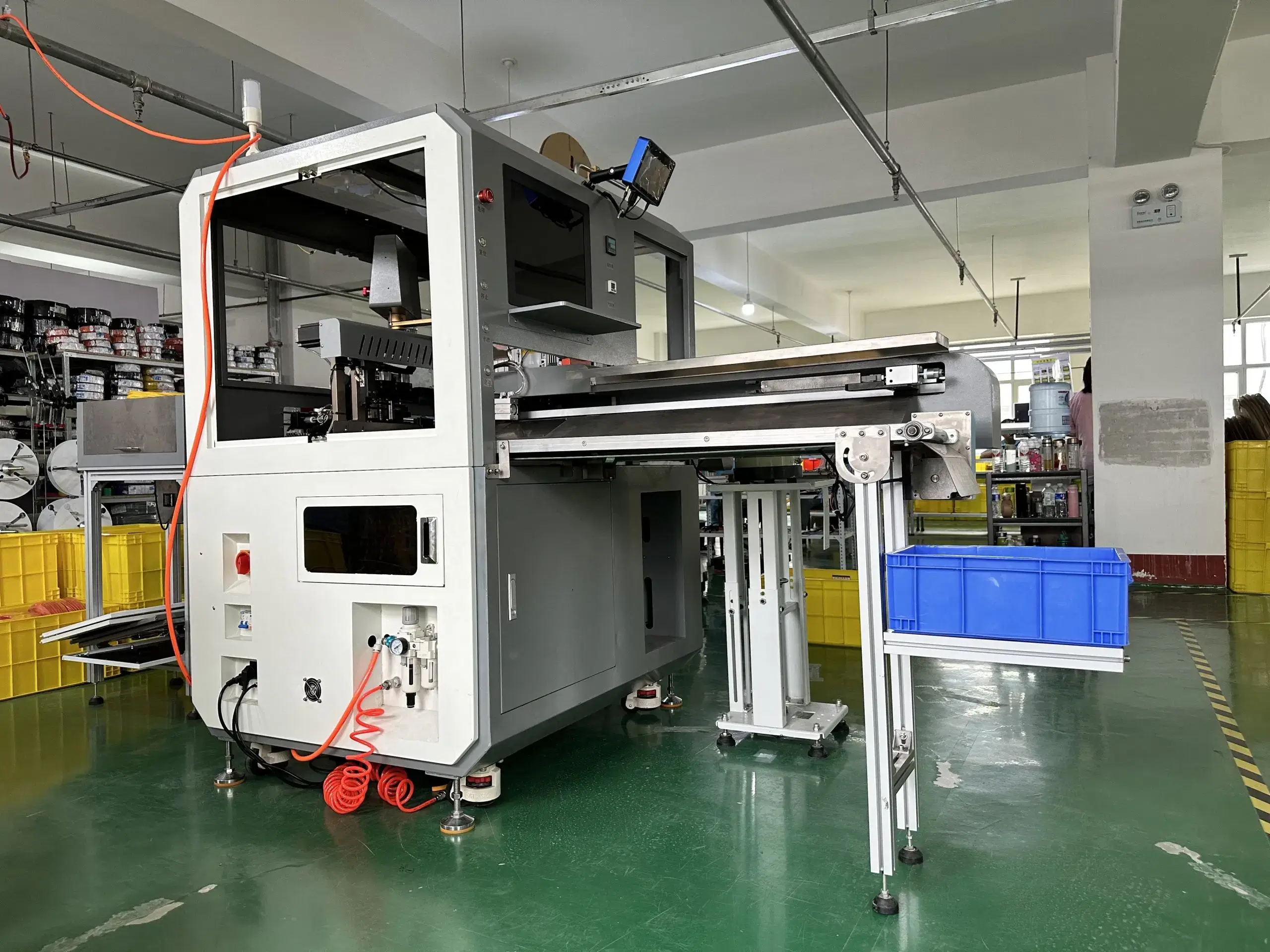
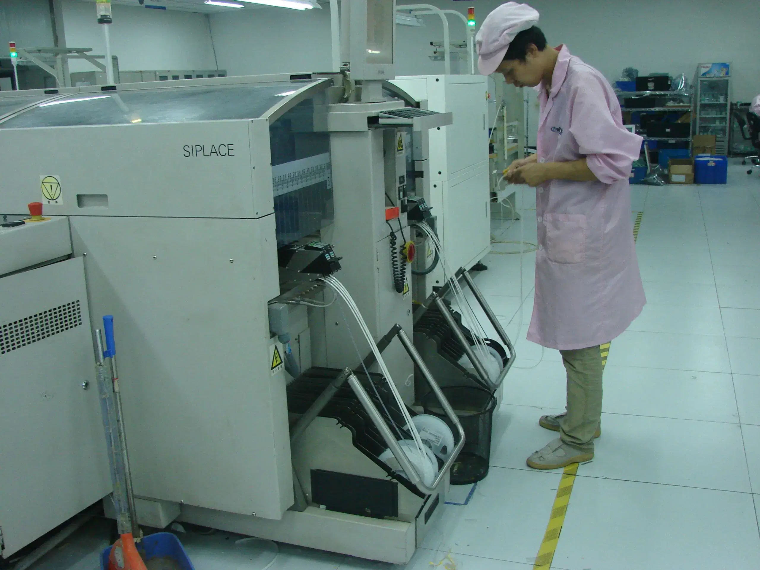
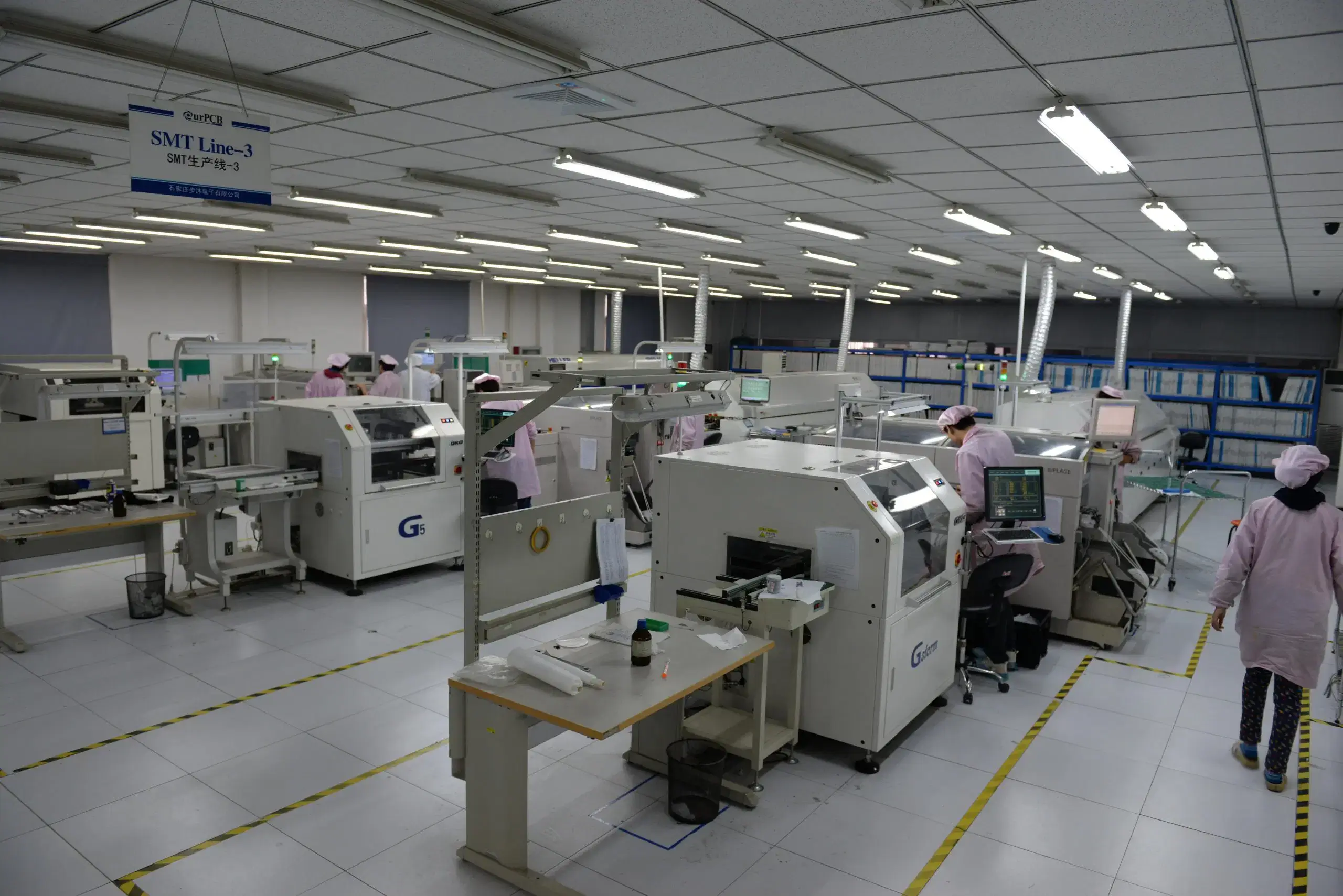
Production assets include 7 SMT lines with Fuji and Samsung SMT mounters for SMT production. Mixed SMT/DIP builds are supported by 4 DIP lines and an auto solder paste screen printer.
Choose The Right Robot PCB Structure
Rigid boards are ideal for stable assemblies with conventional connectors and routing areas, while rigid-flex robot joint boards can provide more flexibility by eliminating connectors between moving or compact joints. HDI robot controller boards are designed to support high routing densities and high pin counts in smaller controllers.
To help manufacturers select the appropriate robot PCB structure for their applications, the following table provides a reference to layer complexity, the typical production position for robotic build conditions, and risk management considerations for selecting the appropriate production position.
| Layer / complexity range | Production fit | Typical robot board use | Risk control |
|---|---|---|---|
| ≤12 layers | Entry multilayer range, not a final capability ceiling | standard controller, I/O, power, communication, sensor boards | stack-up review, drill/plating check, impedance review when needed |
| 13–20 layers | Standard-to-advanced multilayer range as routing density increases | robot controller, communication, multi-sensor interface, compact control platform | controlled stack-up, via strategy, cross-section, electrical test |
| 21–32 layers | Advanced HDI / dense controller range where component density and signal count require it | high-density controller, AI-assisted sensor processing, compact multi-board replacement | HDI stack-up review, laser/mechanical via planning, impedance and yield review |
| 32+ layers | High-layer backplane or complex controller build reviewed case by case | robot main-control backplane, advanced compute/control platform | production confirmation, material availability, lamination/yield review, test plan before commitment |
Heavy Copper For Motor Power
Increasing copper thickness in PCB designs can have consequences during etching, thermal balance, via design, solder profile, and connector heating. All considerations must be made in the design or the process. Heavy copper is not a default specification for a robot PCB board.
Rigid-Flex For Moving Joints
Bend-cycle evidence and continuity data need stated conditions before and after cycling; therefore, there is no one-size-fits-all cycle-life guarantee for every moving joint in a robot.

Robot PCB Assembly Process
The robot PCB assembly process, also known as robotic PCBA, includes approved design files, process control, paste control, placement, soldering, inspection, functional testing, and traceable packing using materials from various suppliers to create a robotic assembly from an approved design.
Engineering File Review
At the initial review, the Gerber or ODB++ file, BOM, centroid, assembly drawings, test requirements, firmware needs, and quantity are checked. The engineer performs checks on footprints, polarity, lifecycle status, approved alternates, and manufacturability before material goes on the line. The result is approved assembly data with component exceptions resolved. This prevents a placement program that is built with a proper setup from creating an incorrect footprint, orientation, or revision during assembly.
Paste Print Inspection
The process for printing solder paste is defined by the stencil, solder paste, panel, aperture settings, and print program used to create the paste print. The ±25 µm solder paste alignment target is part of the paste print process control context and not part of a blanket placement metric.
Fine-Pitch Placement Control
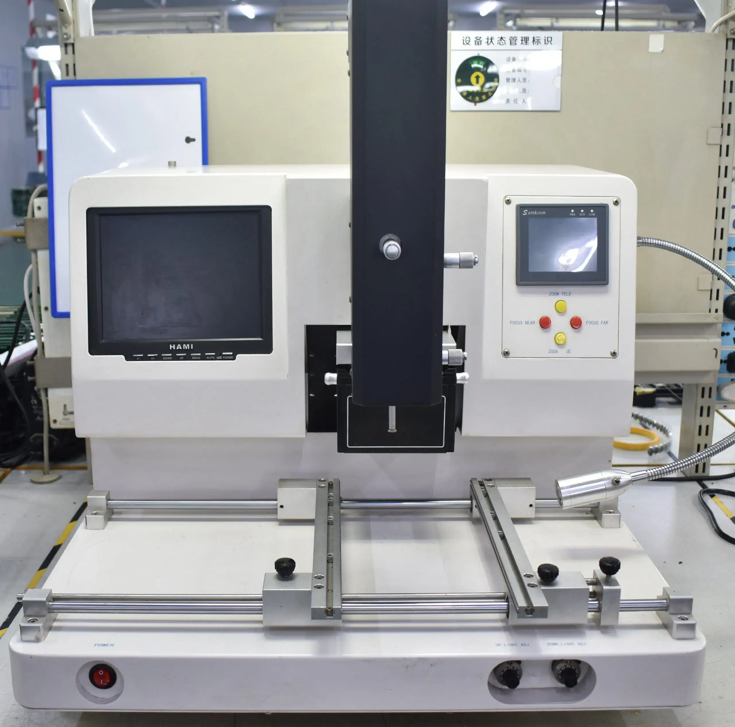
Fine-pitch components, including BGA and 01005, are controlled through verified feeders, moisture control, component reels, placement program, thermal profile, position, and polarity. Controlled reflow joins the components. AOI checks the visible results; if the component is hidden or at risk, it may be X-ray checked. The result is aligned components, acceptable joints, and inspection evidence linked to the first article and active revision.
THT Soldering
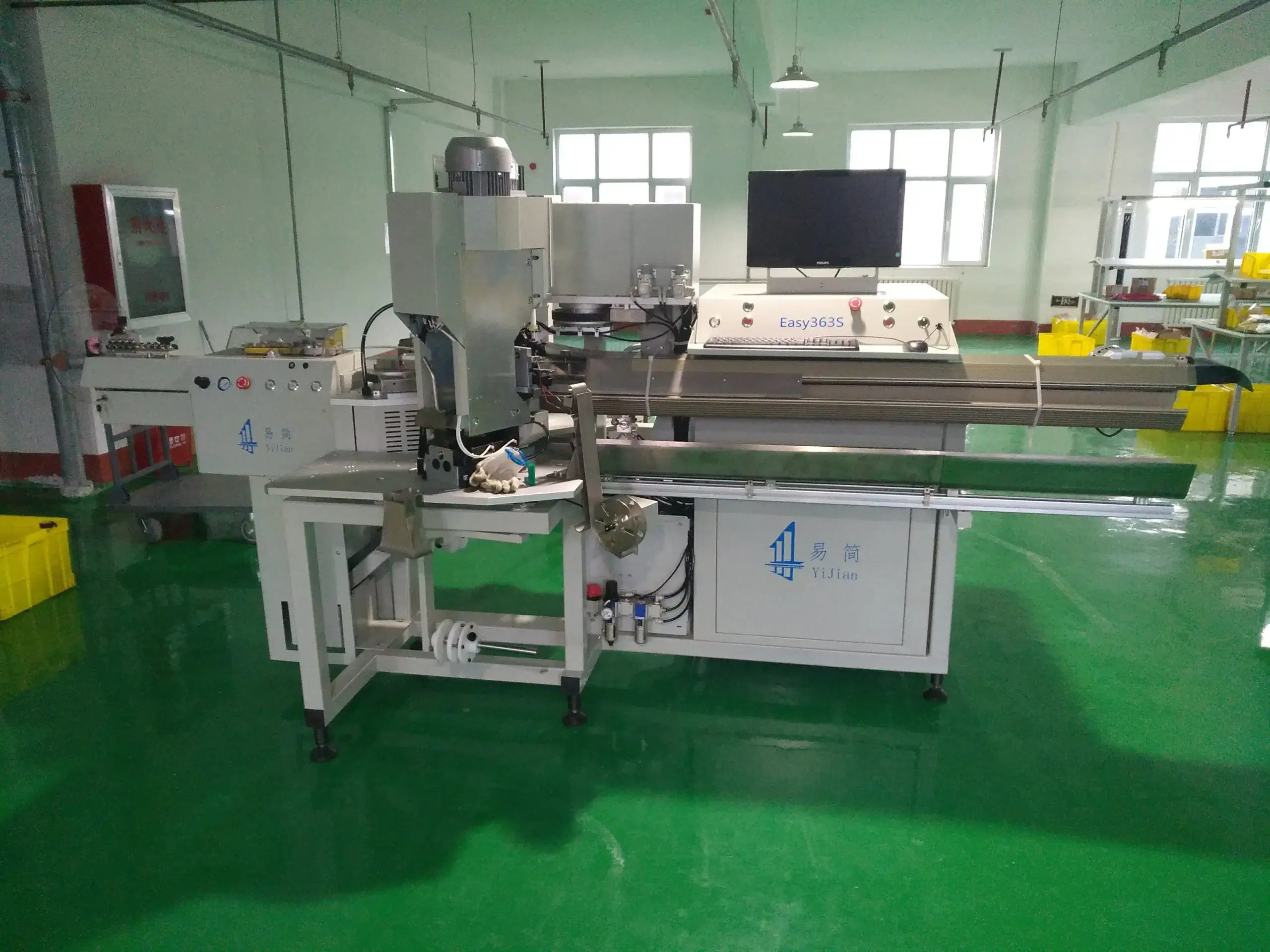
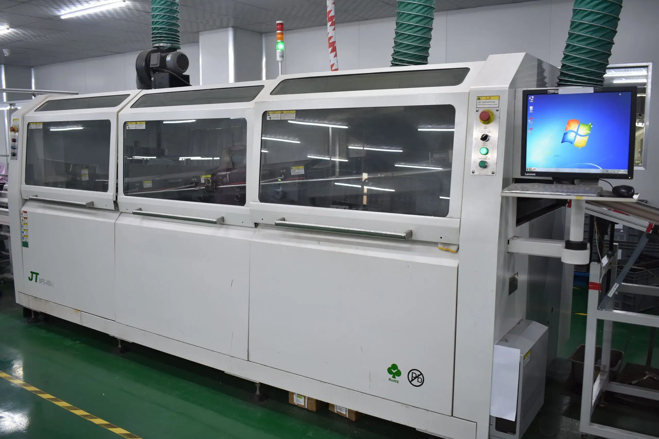
Mixed SMT and THT robot boards typically include connectors, transformers, and power modules. The type of soldering, such as wave, selective, or controlled manual soldering, and masking are selected as part of the assembly plan. As the operator must create mechanically stable joints, care must be taken not to overheat nearby SMT components or starve high-current pins. Records must be maintained during inspection by documenting fill, wetting, polarity, mechanical seating, and connector alignment.
Final Board Test
The final inspection process verifies that the components have been assembled, and then validates the operation of the specified electrical and robot functions. The results will show the board number, revision number, fixture used, and firmware version.
Traceable Packing
Once boards are accepted, they will be packed in ESD-safe materials where appropriate and vacuum sealed where necessary; all packages must contain appropriate labeling. The package label must match the associated lot number and revision number. Packing records provide identification during storage and shipping in addition to safeguarding moisture-sensitive or exposed assemblies from damage during handling.
What Testing Is Needed For Robot PCB Assembly?
Testing of robot PCBs will be performed based on defect visibility, electrical access, functionality, and environmental stress. SPI checks printing before placement, AOI checks visible assembly after placement, X-ray checks hidden joint integrity after reflow, ICT or flying probe checks accessible networks for faults, and final testing verifies defined behavior. A functional test of the motion PCB, HIL test, sensor calibration, protocol testing, or environmental testing applies when applicable to the function of the board.
Which Defects Does SPI Catch?
The purpose of SPI is to measure solder-paste volume, area, height, and alignment. SPI can identify incorrect solder-paste volume, such as insufficient solder paste, excess solder paste, bridging risk, and print offset, before components cover the deposits. The ±25 µm solder paste alignment target should be included in process control. SPI cannot provide proof of component placement, reflow quality, or hidden joint integrity; therefore, it is the first step in the test sequence and not final acceptance.
When Does AOI Miss Hidden Joints?
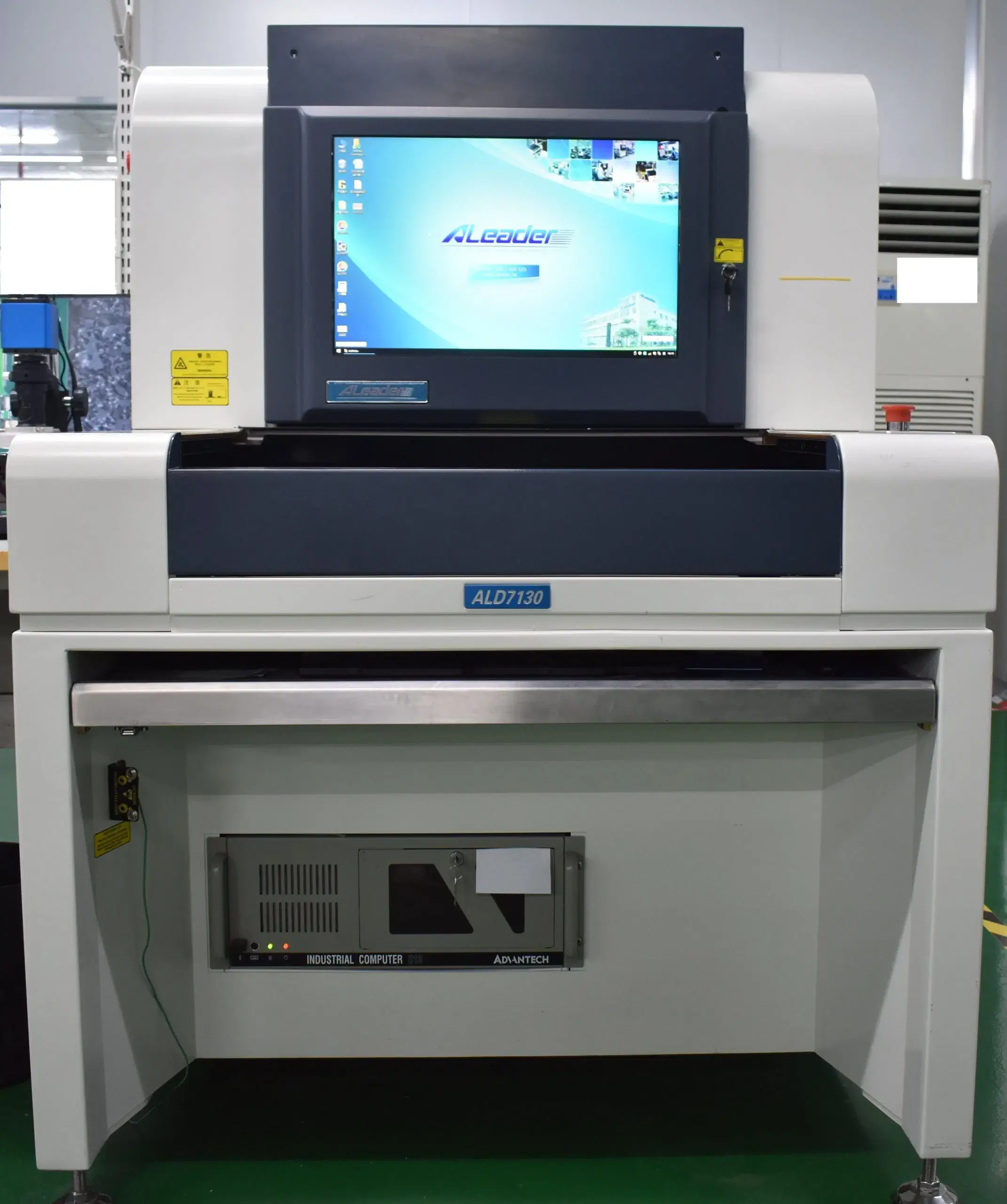
AOI inspection can verify whether components are present, in the correct orientation, aligned within specifications, whether bridges are present, and whether visible solder joints are acceptable after reflow. It cannot verify hidden solder joints beneath BGA, LGA, QFN, and similar bottom-terminated packages. A 100% AOI statement describes inspection coverage for a particular production setup, not a universal requirement for every robotic PCBA. To capture hidden or risk-sensitive solder joints, AOI inspection images must be supported by an escalation rule that sends these joints to X-ray inspection.

Hidden-Joint X-Ray Inspection
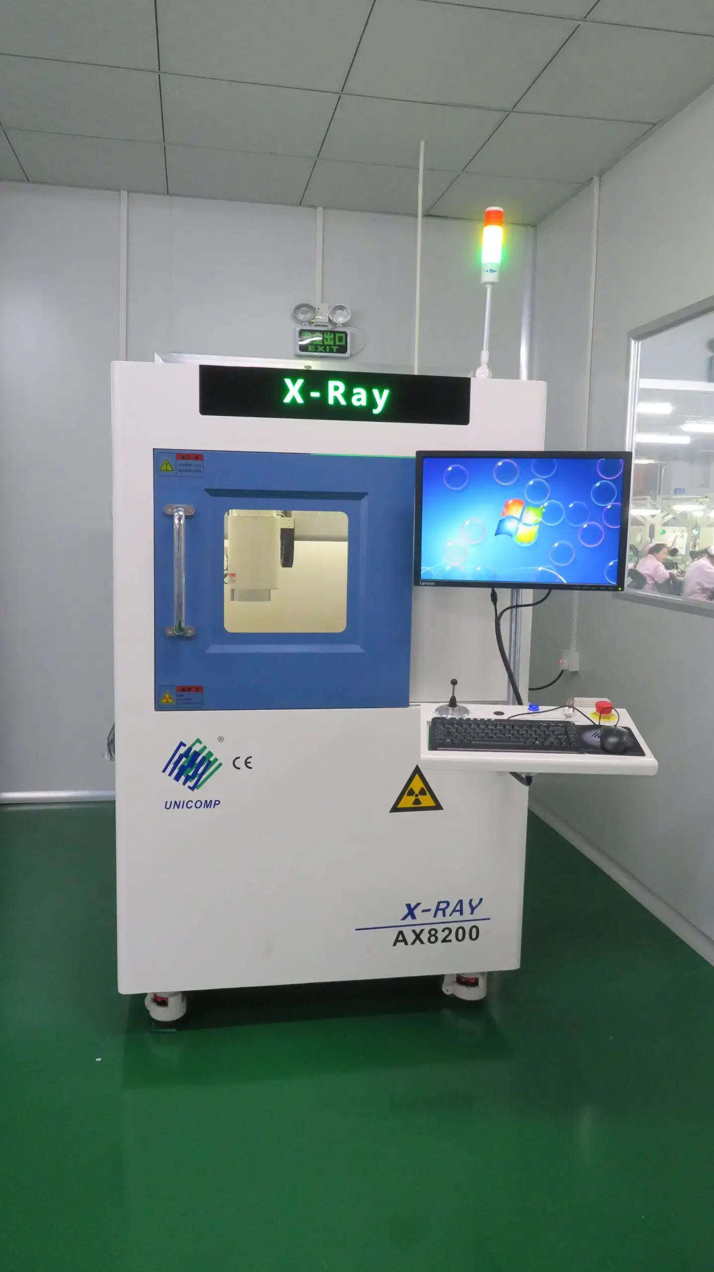
X-ray will reveal ball shape and alignment, opens, bridges, and voids beneath BGA, QFN, or LGA packages. Each package should have specific acceptance criteria that define what will pass inspection, what needs further review, and what requires rework.
ICT For Continuity And Shorts
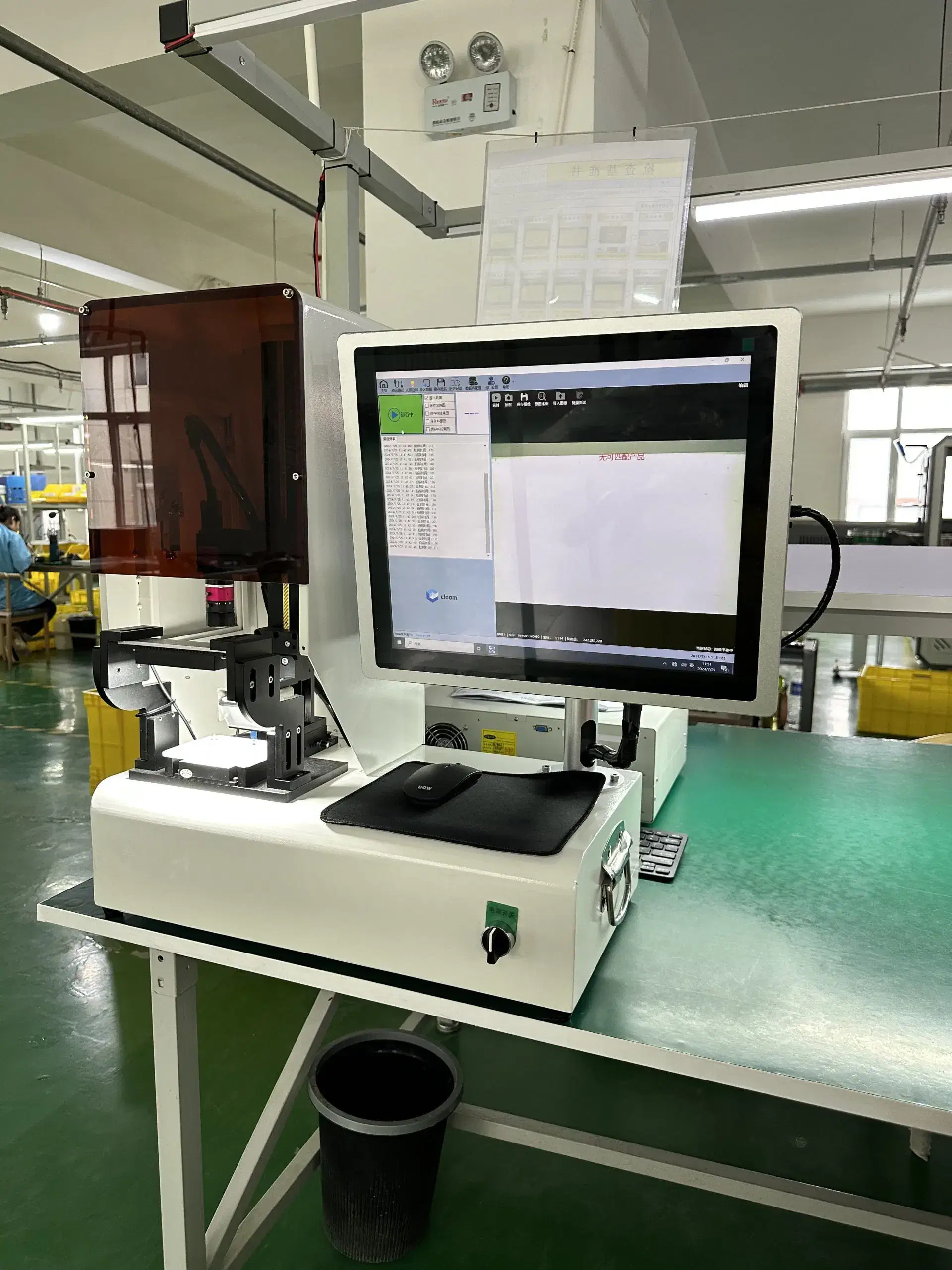
ICT or flying probe testers can verify continuity, shorts, resistance measurement, and accessible circuit nodes. ICT catches electrical network faults that cannot be classified by optical inspection. The results from ICT should identify the PCB revision and the associated test limits. A PCB may pass ICT while firmware, sensor readings, motor outputs, or communication loops still operate incorrectly under normal operating conditions.
Robot Behavior Functional Tests
FCT applies electrical power and tests defined behavior such as rails, I/O states, communications, sensor readings, and motor-control outputs. HIL testing allows controlled inputs and loads when a motion controller needs fixture-driven robot behavior. Sensor calibration tests validate a sensor’s accuracy by comparing the sensor output with a known value, while protocol testing exercises EtherCAT, CAN, industrial Ethernet, or another specified interface.
These tests depend on firmware, fixtures, procedures, customer limits, and revision identity. For each test performed, the limits, software version, fixture identity, results, and pass/fail conclusion should be maintained.
When Does Environmental Testing Matter?
When environmental vibration, temperature, humidity, bend area, connector motion, and duty cycle can characterize similar stresses found in the intended use, environmental testing information is needed. Environmental testing may be used to assess solder fatigue, thermal drift, moisture effects, bend-zone fatigue, and intermittent contacts.
It is essential that the test conditions accurately replicate those of the application for which the product was designed. All test conditions must be documented in terms of condition, duration, sample plan, cycle or load state, and pass/fail status. One test stress sequence should not be applied to every robot cleaner PCB testing or industrial control project.
What Fails First On A Robot Control Board?
The challenges associated with robot control board assembly typically begin where electrical load, mechanical motion, and inspection blind spots meet. Vibration attacks heavy components and connectors, thermal load concentrates around power paths, switching edges disturb sensors, component obsolescence disrupts revisions, and cable motion damages connectors or interfaces.
How Does Vibration Damage Solder Joints?
When a component, connector, or cable is subjected to repeated acceleration, it creates relative movement between the component or connector and the PCB. The excessive load from that relative movement is transferred to the solder joint until the solder joint experiences enough repeated loading to develop cracks or intermittent contact as a result of fatigue. Effective board support for connectors and cables, connector retention, strain relief, and component staking when required help prevent these joint movements.
Testing should be conducted in such a way that the mechanical condition of the installation is exercised and continuity or functional evidence exists before, during, or after applying the stress, as the testing procedure permits.
Where Does Heat Accumulate?
Motor drive devices, compact power conversion, high-current connectors, and restricted copper paths are all points where heat can collect. With excessive heat, solder fatigue can increase, electrical characteristics can shift, or component lifetime can decrease. Copper and thermal designs are used to spread the load, while the assembly profile and thermal interfaces are used to protect the finished copper paths.
A functional load test and temperature results should demonstrate that the selected design, solder process, and components can function under the intended requirements.
How Does Switching Noise Reach Sensors?
Fast power edges can couple into sensor signals through shared return paths, poor separation distance, cable coupling, or weak isolation of the sensor from the power lines. As a result, the sensor output may show false readings, experience unstable control, or have communication errors, even though there may not be any visible defect on the physical PCB.
By planning proper return paths, filtering, reducing coupling between the return path and sensor, and providing shielding as needed, the coupling path is reduced. The system test should therefore operate the power stage while monitoring the affected sensor or communication channel.
What Happens When Components Go Obsolete?
As a product approaches the end of its lifecycle, a late lifecycle notice, allocation, single-source part, or package substitution can require redesign and unplanned validation of the replacement component. When parts are replaced without a controlled method of replacement, assemblies may contain mixed revisions and unclear test coverage. Lifecycle monitoring gives the team time to qualify approved alternatives. Controlled substitution, revision records, and regression tests confirm that the replacement preserves the electrical performance, programming, assembly compatibility, and necessary robot functionality.
Why Do Connectors Fail In Motion?
Reasons for connector failure during motion include mating cycles, cable strain, vibration, and misalignment, which can lead to fretting, intermittent connectivity, solder joint cracks, or pulled pads. Retention and strain relief must keep cable loads away from the solder joint, while alignment controls must prevent forced mating. Continuity and motion tests can reveal intermittent problems that static inspections would not find. The fixture must reproduce the meaningful direction and range of movement instead of just flexing the cable randomly.
Robot PCB Applications
Every robotic application has unique PCB requirements for control, power, sensing, communication, safety, environmental exposure, and acceptance evidence. Grouping PCBs by their requirements creates a separate manufacturing and testing focus for every category of robot.
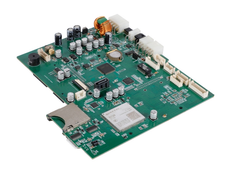
Industrial Robots
Industrial robot controller and drive PCBAs function with deterministic motion control, high-current motor stages, safety I/O, and industrial networking under continuous duty conditions. They are subject to vibration and heat, which create stress on connector retention, solder fatigue, and thermal pathways. Functional testing should include motion commands, communication, and interlocks, instead of treating them as generic digital circuit boards.
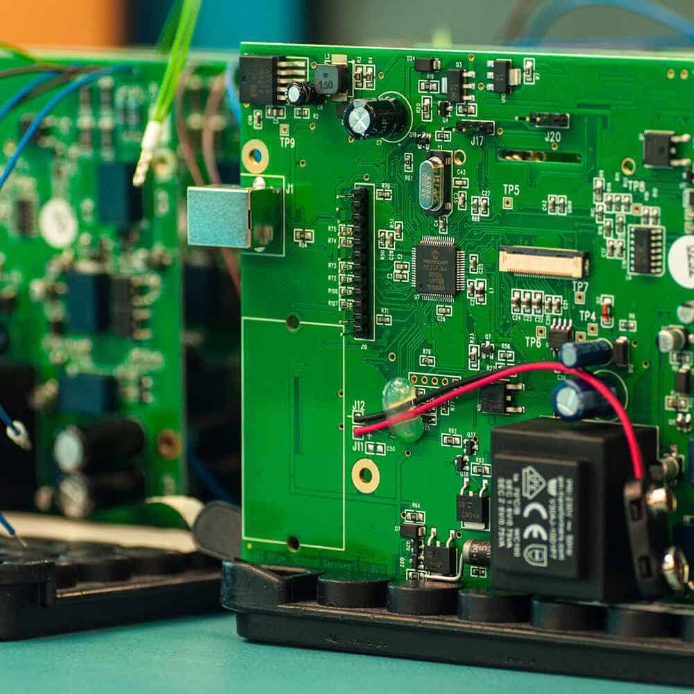
Collaborative Robots
Collaborative robots place motor drives, encoders, force sensors, rigid-flex circuits, and safety functions close to moving mechanisms and human operators. Compact packaging has high thermal density, while repeated bending of flex transitions and connectors creates flex-transition issues and connector failures. Fine-pitch inspection and traceable functional checks are necessary to verifying the sensing and controlled motion of the selected joint architecture.
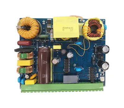
Mobile Robot Systems
The AGV AMR control board integrates navigation control, battery management, motor control, wireless communication, and safety I/O. Mobile hardware is susceptible to mechanical shock, connector movement, and power transients, while fleet production creates increased programming and revision-control risk. To ensure stable quality across multiple batches, the navigation interface, drive behavior, battery charging, communication, and safety states must have stable fixturing and a repeatable method of functional testing.
Medical Robots
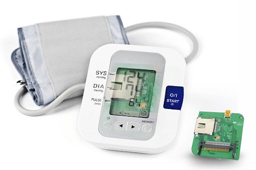
Medical robot PCBAs typically perform precision motion, imaging or sensing, compact controller, and safety functions. All manufacturing evidence must remain separate from regulatory evidence. Fine-pitch inspection, board and lot traceability, controlled revisions, and functional results based on the selected production process are essential.
Service And Educational Robots
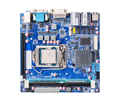
Service robots may combine HMI, sensors, wireless links, batteries, and compact drives under variable duty cycles. Educational boards add safe low-voltage control, repeatable kit assembly, accessible connectors, programmable controllers, polarity protection, and basic function checks. The assembly plan must follow the actual hardware, since a mobile service platform and a classroom kit do not share the same load or acceptance limit.
Agricultural Robots
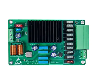
Agricultural robotics PCB assemblies are exposed to dust, moisture, vibration, motor loads, and long or uneven duty cycles. Coating and enclosure choices must align with connector sealing and thermal pathways without trapping contaminants or heat. Environmental and functional evidence should reflect field operation for control, navigation, power, and communication boards.
Cleaning Robots
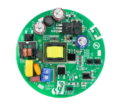
The PCBAs of vacuum robot cleaners, including the robot vacuum control PCB, integrate navigation sensors, wheel and brush motor controllers, battery charging, obstacle detection, and wireless control. Cost control should not affect motor-current soldering, connector durability, programming quality, or end-of-line checks. Movement, charging, and sensor-response testing provide more useful evidence than inspection alone for robot vacuum cleaner PCB assemblies.
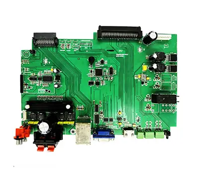
Humanoid And AI Robot Systems
Humanoid robot PCBAs and AI robot PCBAs comprise many components, including joint drives, sensors, power converters, communication, local control, high-density compute, memory, and sensor fusion, to create moving assemblies. High-density packaging coupled with repeated flexing creates concentrated heat and connector fatigue. BGA inspection, power integrity, synchronization links, communication verification, and scalable test coverage must work across the multi-board platform, not as isolated checks on each board.
Prototype To Volume Production
Volume production varies greatly; some designate volume production as between 10 units to several thousand units, while others define mid-volume production as 10,000–50,000 units. No volume range is universal or establishes the minimum order quantity or maximum production limits.
A manufacturer must know the context of the capacity data. For example, capacity may be represented as CPH; however, the CPH figure cannot be directly translated into boards per hour. The estimated number of boards produced per hour is determined by taking the number of effective placements per hour, dividing it by the number of placements on each board, and then accounting for line balancing, changeover, first-article inspection, inspection, yield losses, fixture time, and packaging. 18 SMT production lines and 24-hour PCBA capability establish production availability based upon comparable conditions and not guaranteed delivery for every design.
Prototype Validation
An AI robot PCB prototype or prototype robotics PCBA should expose, in the quickest way possible, any gaps in design, assembly, programming, and test coverage. Early findings may prompt controlled changes to be made; thus, prototype findings may necessitate changes to component footprints, components, firmware, or fixture assumptions. A 24-hour PCBA timeline is meaningful only if the conditions for PCB assembly, material availability, BOM condition, firmware, and test requirements can support that timeline.
Pilot Run Change Control
A pilot run establishes that a method is reproducible before scaling. The team should freeze critical materials, solder profiles, inspection limits, firmware and board revision identity, and fixture assumptions while clearing any remaining discrepancies. As with any pilot, changes can occur; however, all changes must have assigned ownership, established revision control, and a clear impact on inspection or testing.
Mid-Volume Repeatability
Mid-volume robotics PCB assembly is a balance between recurring batches and engineering flexibility. Stable sourcing, fixtures, defect trends, traceability, and revision control should allow consistency when building robotics boards.
High-Volume Process Control
High-volume robotics PCB assembly relies on line balance, automated inspection, fixture capacity, yield trends, controlled sampling where applicable, change governance, and packing traceability.
How To Choose A Robotics PCBA Manufacturer?
Choosing a robotics PCBA manufacturer or robotics-grade board supplier should depend on the compatibility of the production process, traceable evidence, engineering ownership, certificate scope, and scaling controls for the actual robot board. Equipment lists and generic quality statements are weak evidence when they cannot be tied to a site, revision, lot, fixture, or build condition.
Board Capability Match
Board capability is determined by confirming that board structure, package pitch, copper, layer count, assembly mix, programming, and testing can remain compatible throughout the production process. A factory robotic PCB program can fail at one unsupported constraint even when the supplier handles the remaining work. Confirm how rigid-flex, HDI, fine-pitch, high-current, mixed assembly, and required tests connect across the selected production process.
Risk-Matched Inspection Reports
SPI, AOI, X-ray, ICT, and FCT reports should all relate to specific defects or functions and provide the board number, revision number, lot number, acceptance limits, fixture used, and inspection results. Generic samples have very little value. Suppliers should provide information that proves each record is from the production batch and show that exceptions were reviewed.
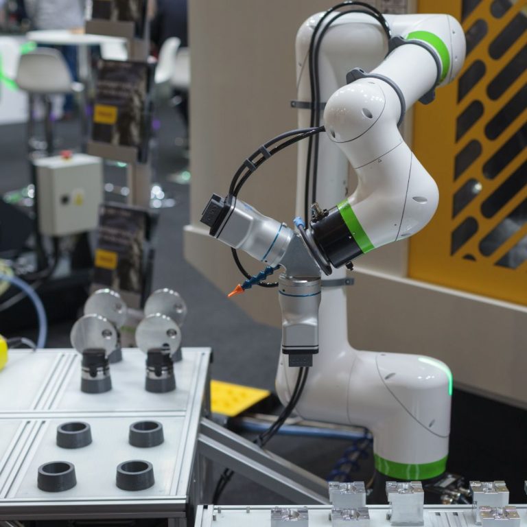
Engineering Support Ownership
Engineering support and ownership include DFM, sourcing changes, programming, fixtures, failure analysis, inspection and testing procedures, and revision-control issues. When a footprint conflict, component change, or function-test failure happens, named escalation paths allow faster resolution. Lack of technical ownership between sales and engineering can create confusion in change history and accountability.
Certificate Match To Actual Production
Before a certificate can be attributed to the actual product being manufactured, validation must include the certificate holder, manufacturing location, scope, certificate validity, acceptance class, and production process. IPC-A-610J covers electronic assembly acceptability where specified, and IPC J-STD-001J applies to soldered electrical and electronic assemblies where specified. IPC-A-600M, IPC-6012F, and IPC-6013E address bare-board, rigid-board, and flex or rigid-flex requirements where applicable. IPC-7711/21D applies to relevant rework, repair, and modification.
IPC-A-610 Class 3 wording should be stated in reference to a customer-defined acceptance class only. It should not be used as a default for every assembly produced on a robotic assembly system. RoHS, REACH, and UL apply when the customer program, target market, material, or product requirement calls for them.
Scaling From Prototype To Repeat Production
Prototype learning, processes, and fixtures must remain intact when scaling through the pilot and repeat-production phases. Fixture continuity, test coverage, automated inspection, traceability, yield trends, sourcing stability, and change control must be monitored at each production phase.
Our PCB Factory Gallery
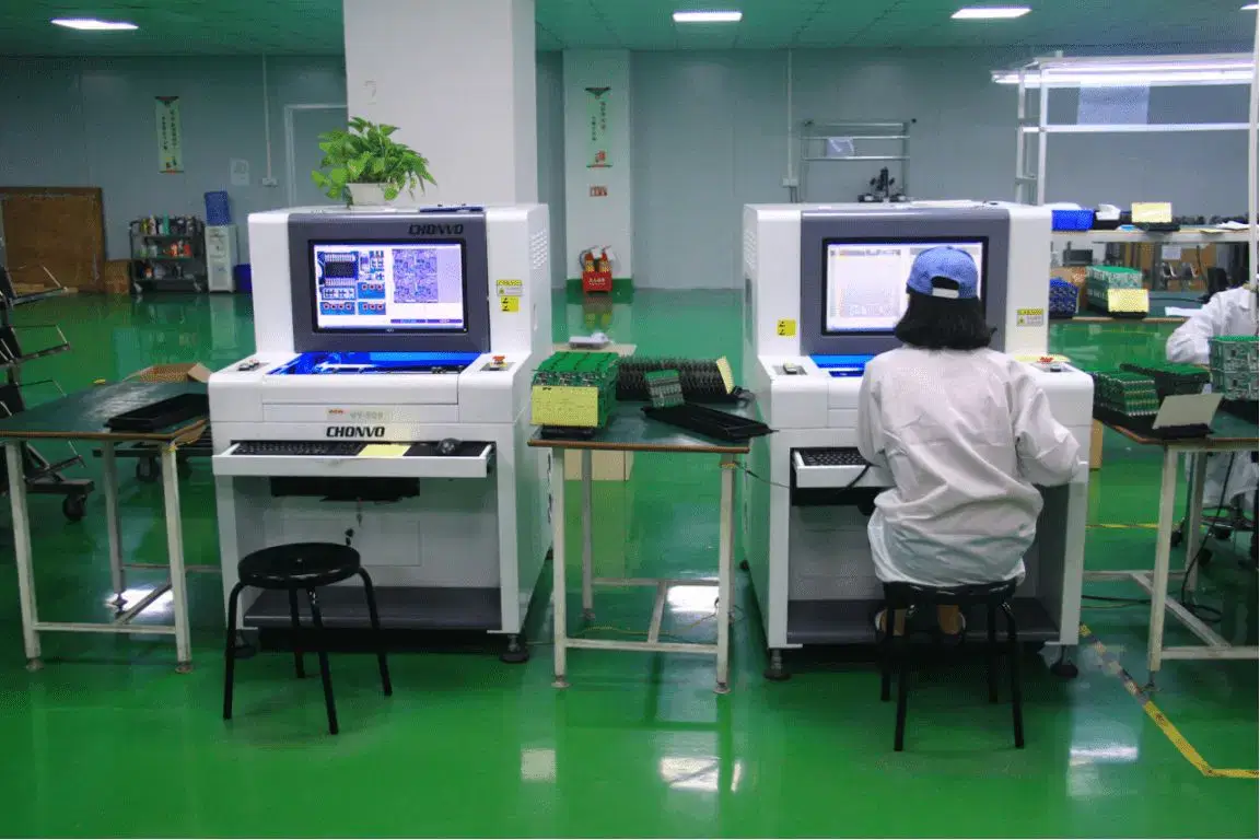
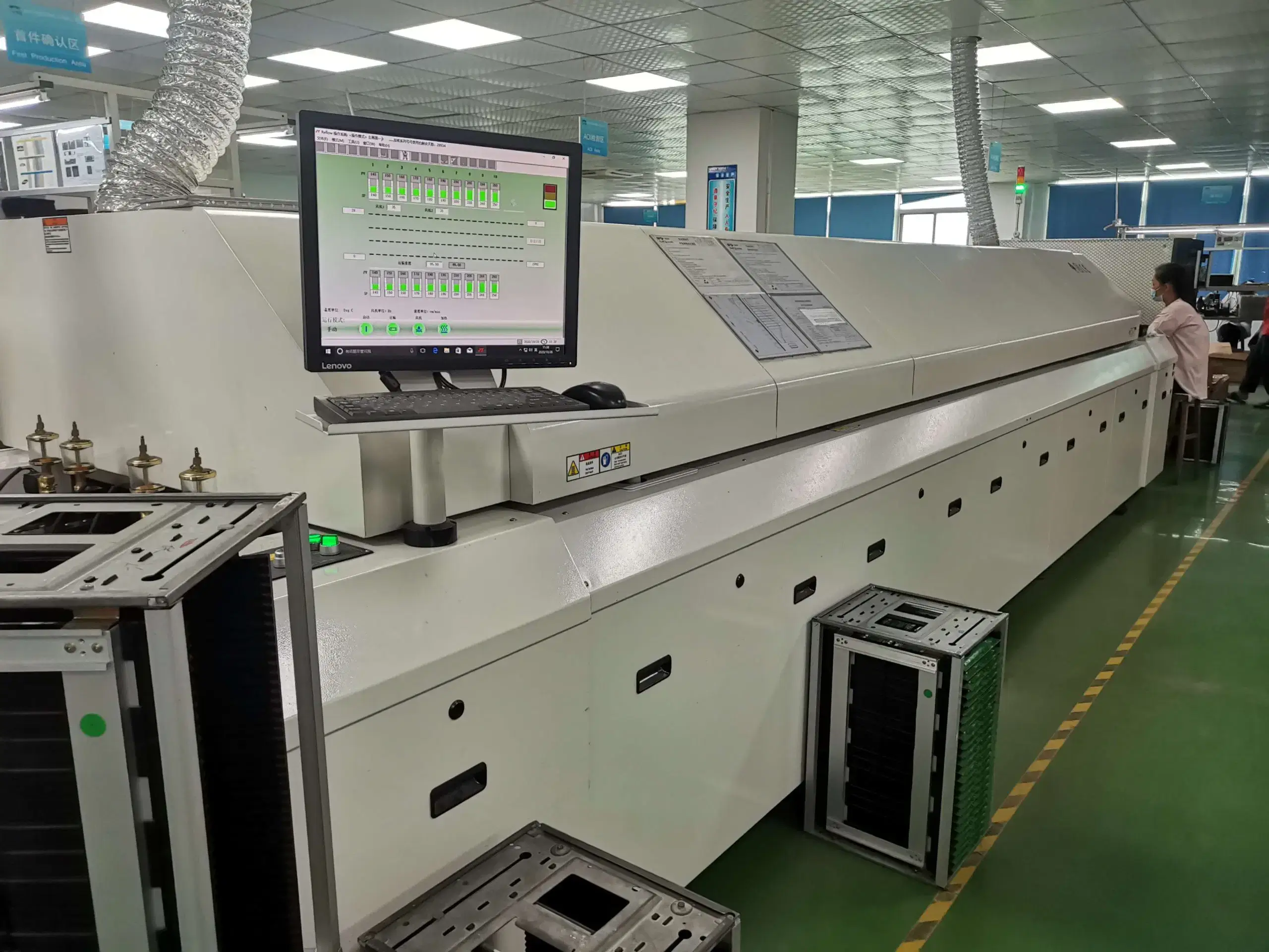
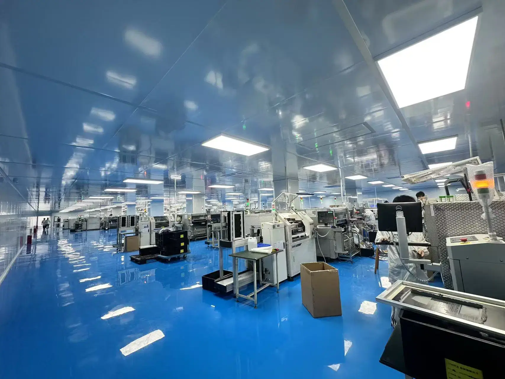
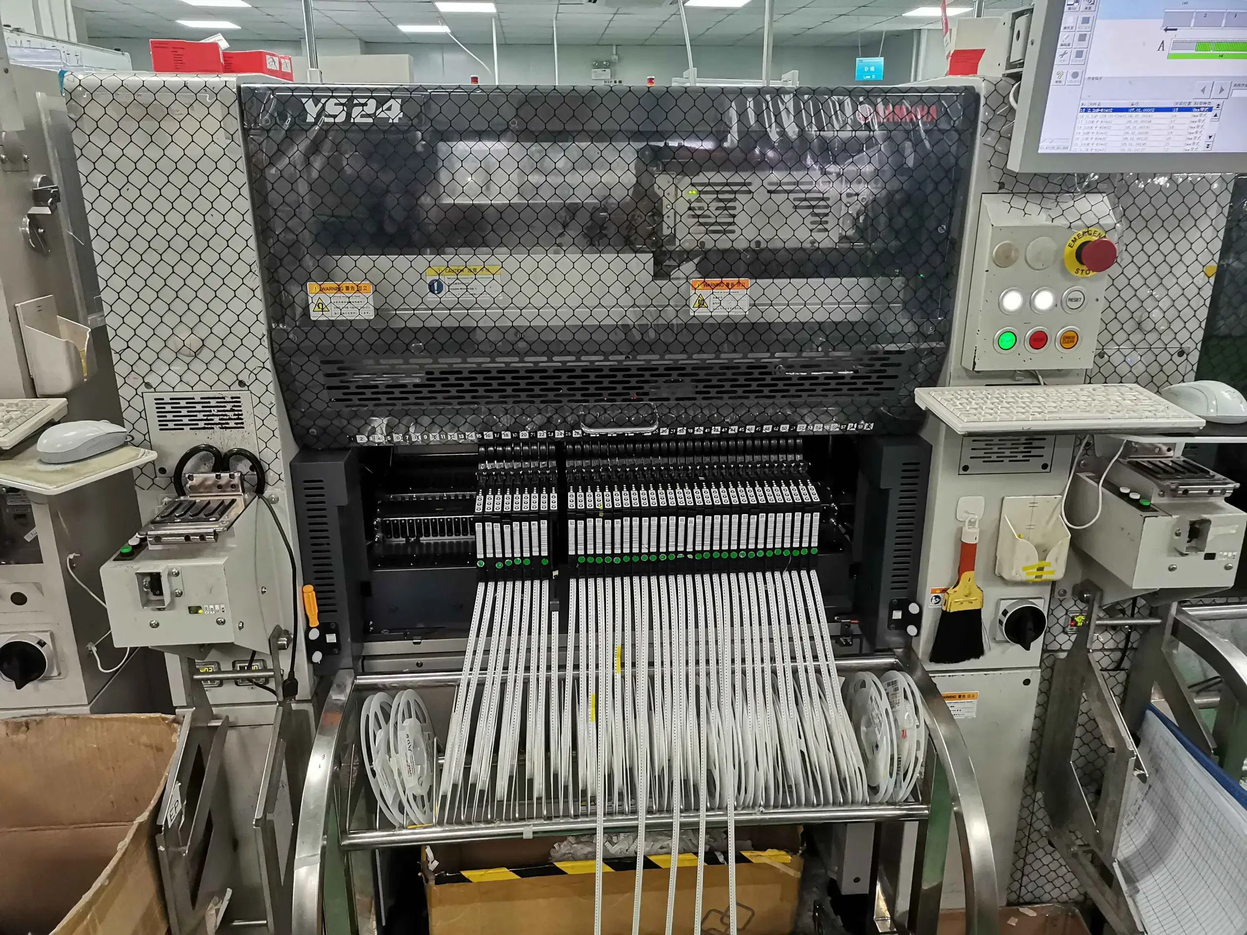
FAQ
Yes. Dense SMD can be used with THT connectors, transformers, or high-current parts that require stronger mechanical attachment to the board. When designing the assembly plan, the assembly method and process must be coordinated. The assembly must use reflow soldering with other methods such as wave, selective, or controlled manual soldering, and each joint type must be inspected according to its visibility and load.
Cost depends on layer count, material, copper weight, package density, component sourcing, SMT/THT mix, programming, test coverage, fixture maturity, volume, and revision frequency. Dense HDI, rigid-flex, heavy copper, hidden-joint inspection, or a new functional fixture changes the production work, so a fixed price without those details is not meaningful.
There is no useful universal MOQ for robot PCB assembly. The practical batch size used for production will vary based on tooling, material procurement, test setup, sourcing stability, inspection planning, and process-control maturity. Prototype and repeat-production quantities should be chosen based on the work needed to build and verify the board consistently.