Upload BOM & Gerber
-
Mobile: +86 13312967631
-
Email: sales@sugaintl.com

PCB Manufacturing Tolerances
Turn PCB Tolerances Into Measurable Results
A fabrication-drawing tolerance becomes a production requirement when the finished board can be measured against it. SUGA connects feature-specific engineering checks, process controls, dimensional and optical inspection, microsection, and TDR across its Shenzhen and Pearl River Delta production network. Each requirement is tied to a named feature, finished condition, drawing revision, and acceptance result.
±5% / ±10%
controlled-impedance bands for approved stackups, covering tight and standard targets.
0.15–6.5 mm
mechanical drill range; the 0.15 mm limit applies to board thickness ≤1.2 mm.
±0.05 / ±0.075 mm
tolerances for NPTH and PTH.
Up to 40 layers
multilayer PCB capability through SUGA-managed production.
What Are PCB Manufacturing Tolerances?
PCB manufacturing tolerances establish an acceptable amount of deviation from the specified dimensions for finished PCB features. A minimum hole diameter or trace width is an example of an established process limitation, while a drawing tolerance represents the acceptance criteria for finished PCBs.
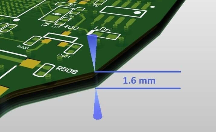
For example, at the time of incoming inspection, the nominal thickness of the PCB is 1.60 mm, and acceptance is defined within a ±10% tolerance band of the nominal thickness. Additionally, the manufacturing range for this nominal thickness may include thinner designs that are manufacturable. While each of these numbers has a specific purpose, using them interchangeably can lead to disputes over the rejection of a finished PCB even when the board is manufactured within the approved process window.
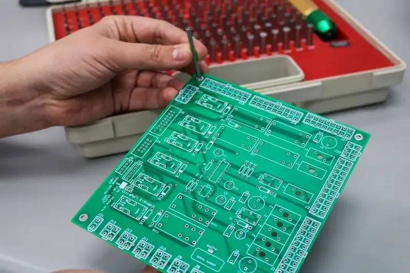
| Requirement type | Engineering definition | Typical PCB callout | Verification basis |
|---|---|---|---|
| Nominal | Target dimension in drawing or stackup | 1.60 mm finished thickness | Fabrication drawing / approved stackup |
| Acceptance band | Permitted variation around nominal | 1.60 mm ±10% | Dimensional inspection result |
| Process minimum | Manufacturable limit under stated conditions | Minimum drill or trace/spacing | Engineering capability assessment |
| Standard production window | Repeatable range for routine fabrication | Standard routed outline or hole tolerance | Standard inspection report |
| Tight production window | Narrower range for function-critical feature | Press-fit hole, laser profile, ±5% impedance | Feature-specific measurement |
| Design guidance | Geometry used to improve yield and process stability | Copper-to-edge or mask web recommendation | DFM result |
| Process-layer range | Thickness created by plating, finish, or ink | ENIG layer or solder-mask thickness | Process control / XRF / microsection |
How Do Fabrication and Assembly Tolerances Differ?
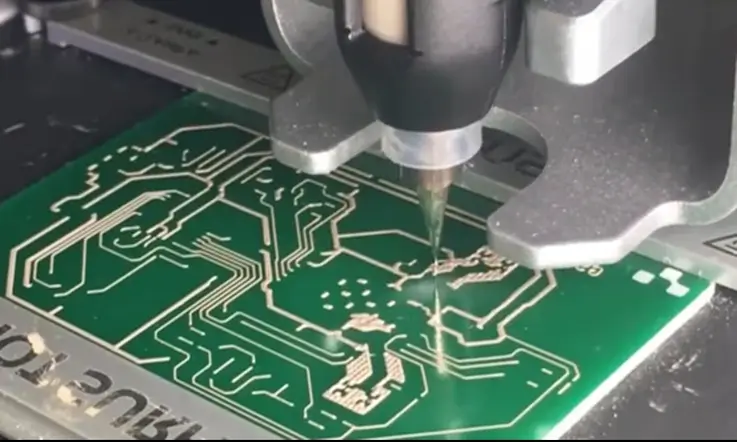
PCB fabrication tolerances govern the manufacture of a bare board: outline, thickness, finished holes, copper geometry, solder-mask registration, and impedance.
In contrast, assembly tolerances govern component position, component rotation, solder deposition, and placement alignment. Pads, connector holes, and board edges are interface features, but fabrication and assembly tolerances remain separate.
The fabrication tolerances of through-hole connectors define finished-hole diameter, annular-ring width, pad geometry, and board-edge location; however, the assembly tolerance for the same connector defines lead entry, component seating height, and overall component position. Therefore, a fit issue can arise from a correct connector being located on an incorrect hole pattern, or because the holes are correct but the assembly is not aligned properly. The drawing and inspection plan must allow the source of the problem to be identified.
Why Nominal Dimensions Need Acceptance Bands
A nominal dimension represents a target for manufacturing and measurement; manufacturing processes and measurement methods both create variations from the nominal dimension. Therefore, the drawing must include the range that maintains form and function when variations occur. Bilateral tolerances allow symmetric variations around the nominal dimension; unilateral limits represent minimum clearance, maximum material thickness, or another constraint in one direction.
Datum selection and the finished state of the part should always be considered when establishing the nominal dimension. A routed profile measured from one origin may yield a different positional result from features controlled through chained references. In the case of connector edges, housing interfaces, and hole patterns, one functional datum scheme prevents tolerance accumulation from being concealed across separate dimensions.
When Are Standard or Tight PCB Tolerances Appropriate?
Standard tolerances can be used for routine thicknesses, dimensional profiles, mounting-hole locations, conventional routing, and non-critical solder-mask applications, as long as electrical function and mechanical assembly remain within a stable production window.
Tighter tolerances should be used for connector edges, precision housings, press-fit features, critical hole locations, local fine geometry, and ±5% impedance when fit, insertion, signal integrity, or local reliability is sensitive to those parameters. Special requirements include laser profiles, complex HDI, stacked vias, very thin boards, heavy copper with fine geometry, and local thickness conditions outside the normal production window.
The same numerical value can represent different difficulty levels. For example, a 0.05 mm value represents a standard finished NPTH tolerance in this capability set. However, it may also represent a tight profile or registration target. The unit of measure, board construction, feature size, datum, and inspection method determine whether a 0.1 mm tolerance is considered standard or demanding.
Standard vs. Best-Case Tolerances
Standard capability represents a repeatable production window. Best-case capability is the tightest result attainable for a defined construction, production method, panel design, and inspection condition. However, for individual features that are critical to the function of the entire assembly, a tighter tolerance should be reserved in the drawing.
For example, laser-routed profiles, press-fit holes, and ±5% impedance may all constitute tight tolerances, but the controls used to achieve these results are not interchangeable. Profile accuracy is determined by variables including board thickness, datum, fixturing, and edge processing. Press-fit function depends on the finished-hole size and plating condition. Impedance depends on material properties, stackup design, copper geometry, and a representative TDR coupon. For specialist processes, the material, production method, equipment class, inspection frequency, and lot records must all be established before fabrication.
How Should Tolerances Be Stated on Fabrication Drawings?
Fabrication drawings should state the feature name, nominal value, units of measure, finished condition, datum, tolerance direction, and inspection method. Routine callouts usually identify the feature name, nominal value, and production tolerance. Callouts identifying tight tolerances should include the finished condition, datum, limit, and inspection method. Special callouts should identify the board construction, process conditions, and type of lot report required. For example, distinguish between PTH and NPTH, drill-tool diameter and finished-hole diameter, and controlled impedance and geometric dimensions.
A general note indicating “tight tolerance” is not sufficient. It is necessary to state the feature to which the specific tolerance applies and how it affects fit, signal, insertion, reliability, or incoming inspection.
Bilateral limits are appropriate for dimensions that can vary equally in both directions. Conversely, unilateral limits apply to dimensions for which only minimum clearance, maximum thickness, or another limit in one direction protects function. Controlled-impedance callouts should also identify the line type and stackup because the transmission-line construction determines the electrical response.
Why Do Tight Tolerances Cost More?
The increase results from changes in process compensation, equipment, inspection frequency, panel utilization, and scrap exposure.
Mechanical profiles and finished holes may require dedicated compensation, first-article measurement, and more frequent dimensional checks.
Fine copper, mask webs, and tight impedance also require additional imaging, plating, stackup, coupon, and lot controls. In addition, specialist processes may lock in the material, equipment, panel orientation, and inspection sampling used for each lot. Setting the tightest limits across the entire board may reduce the usable panel area or increase the potential for rework or scrap.
Function-critical tolerances should remain the same from prototype through production. Therefore, the narrowest limits should apply only to local features that affect fit, signal, insertion, or reliability. Unrelated features can remain within the standard window and avoid the additional expense of the most demanding process.
Board Thickness and Mechanical Dimensional Tolerances
Finished Board Thickness
The finished thickness of the board includes the laminate, copper, plating, solder mask, and surface finish. Construction ranges and acceptance bands should remain separate. Local stiffeners and gold-finger areas of flexible designs should have their own measurement locations. Average measurements across the entire board may mask a thickness issue in a connector zone.
| Feature | Capability / acceptance limit | Application condition |
|---|---|---|
| Finished board thickness | 0.60–3.20 mm range | Construction range; specify acceptance band separately |
| Finished thickness, material ≤1.0 mm | ±0.10 mm | Stated board construction |
| Finished thickness, material >1.0 mm | ±10% | Construction assessment for tighter limits |
| Flexible PCB thickness | ±0.025 mm; stiffener area ±0.05 mm | Separate flex-area and stiffener measurements |
| Routed profile | ±0.13 mm standard; ±0.076 mm tight | Drawing datum + routed-profile method |
| Laser-routed profile | ±0.025 mm for panels below 0.81 mm (0.032 in) | Thin-panel laser-routing condition |
| Bow and twist | 0.75% with SMD; 1.5% without SMD | Board size + defined diagonal measurement method |
| V-score position / residual | ±0.10 mm position; 0.50 mm ±0.10 mm residual | V-score process |
| Bevel | ±5° angle; ±0.10 mm remaining material | Defined connector edge |
| Copper-to-edge clearance | ≥0.20 mm to CNC-routed edge; ≥0.40 mm to V-cut line | Design clearance; profile acceptance set separately |
| Internal routed slot width | ±0.10 mm at width ≥1.0 mm; ±0.15 mm below 1.0 mm | Finished slot width; define datum and pin-gauge, CMM, or optical method |
| V-score breakout edge | ±0.20 mm | Finished edge after depaneling; panel design and board thickness specific |
| Profile-to-copper clearance | 0.30 mm standard; 0.25 mm tight | Finished routed or laser edge; local tight value identified on drawing |
PCB Bow and Twist
Bow and twist in the finished PCB result from multiple factors: copper balance, construction symmetry, moisture, PCB panel handling, and surface-mount content. Bowed or twisted PCBs can cause issues with solder-paste printing, component placement, connector fit, and fixture contact.
The percentage of bow or twist is only meaningful when taking into consideration other factors such as board size, diagonal or edge reference, support conditions, and the agreed measurement procedure.
How Do Edge Processes Affect Copper Clearance?
Edge processes, including CNC routing, laser routing, V-scoring, and beveling, each leave unique edge conditions on the PCB. Different edge processes require a matching profile value, board-thickness range, datum, and inspection method.
Copper clearance is maintained based on the separation method. Copper clearance protects conductors during profiling or depaneling, while outline tolerance dictates the finished edge position. Even though a PCB meets the outline dimension, copper may be exposed if the clearance requirement was designed independently of the selected edge process.
PCB Hole and Annular Ring Tolerances
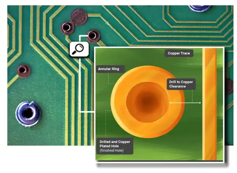
PCB hole tolerance begins with the hole family and finished state. The finished-hole size of a PTH includes hole-wall plating; the size of an NPTH is measured without plated-wall buildup. The position of the hole dictates the remaining annular ring and the fit of the mating connector.
The entire functional relationship can be expressed as drill-tool diameter, plating allowance, finished-hole diameter, positional variation, annular ring, and connector or mounting fit. All of these values should be defined and measured independently; a correct drill tool does not guarantee a correct finished-hole size.
Finished Hole Size and Plating Allowance
Finished-hole tolerance describes the finished diameter; drilling compensation is a process input.
| Feature | Capability / limit | Control condition |
|---|---|---|
| Mechanical drilling | 0.15–6.5 mm | 0.15 mm minimum at board thickness ≤1.2 mm |
| Finished PTH diameter | ±0.075 mm | Measure after hole-wall plating |
| Finished NPTH diameter | ±0.05 mm | No plated-wall allowance |
| Minimum NPTH diameter | 0.40 mm | Mechanical or mounting feature |
| Minimum slot width | 0.50 mm | Identify plated or non-plated wall |
| Minimum castellated-hole diameter | 0.50 mm | Board-edge solder interface |
| Blind-via wall copper | ≥20 μm | Stated HDI construction |
| Laser blind-via dimple | ≤10 μm | Laser-via process |
| Via pad allowance, single side | ≥0.10 mm | Finished-hole + registration allowance |
| PTH pad allowance, single side | ≥0.20 mm | Finished-hole + registration allowance |
| Annular-ring design input | 3.5 mil at 1 oz; 4.5 mil at 2 oz single-side | Hole family + registration + breakout rule |
| NPTH-to-copper clearance | 0.20 mm standard; 0.15 mm tight | Finished NPTH edge to adjacent copper |
Using a 1.000 mm PTH with a tolerance of ±0.075 mm gives a minimum and maximum acceptance value of 0.925 mm and 1.075 mm. Using a 1.000 mm NPTH with a tolerance of ±0.05 mm gives an acceptable range of 0.95–1.05 mm. For press-fit and mating-pin interfaces that require a precise fit based on finished-hole diameter, the limits will be narrower and use a feature-specific inspection method.
PCB Hole Structures
PTH holes must maintain continuous hole-wall copper and barrel integrity throughout the manufacturing process. NPTH holes provide mechanical clearance without plated-wall buildup. Plated and non-plated slots may have the same minimum width, but they are distinctly different finished features because of differences in wall conditions, gauges, and acceptance records.
When using laser microvias, additional requirements are based on dimple size, capture-pad width, dielectric depth, and via registration. The copper and dimple values specified in the drawing correspond to the approved HDI construction; using a different dielectric material or sequential-lamination method can change the manufacturability of the same nominal via.
How Much Annular Ring Is Needed?
Annular ring is the amount of copper that remains around the finished hole after drilling and layer registration. The pad size must accommodate the finished-hole size, plating allowance, positional margin, copper weight, applicable IPC class, and permitted breakout condition. A larger nominal pad does not remove the need to verify that adjacent copper has the required clearance.
Trace Geometry and Copper Thickness
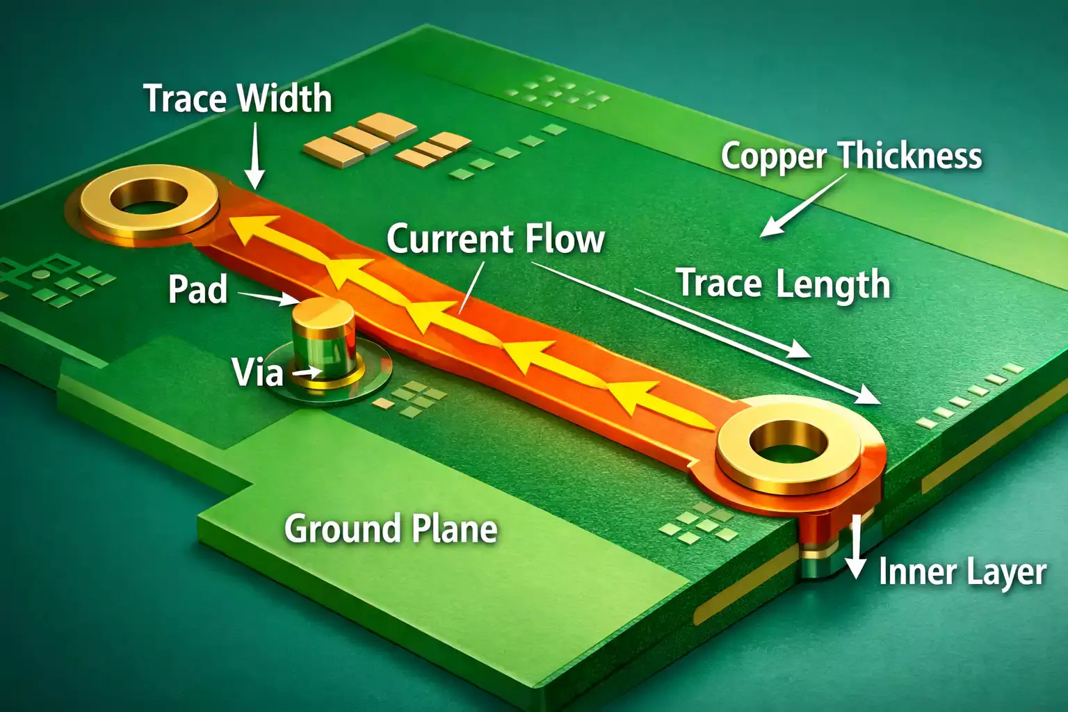
PCB trace-width tolerance, trace spacing, copper thickness, and minimum manufacturable geometry are separate measurements. As copper weight increases, the additional etch compensation affects the practical trace-spacing window and minimum manufacturable geometry. A 4/4 mil capability defines a manufacturable trace-width and spacing limit but does not automatically define the finished width of a controlled conductor. Drawing requirements for conductor geometries controlling current, timing, or impedance have their own finished-geometry tolerances. Inner and outer layers use different imaging and plating processes, so their geometry limits should be assigned separately.
Trace Width Limits
When selecting trace geometry, copper weight, layer position, and production class should be considered. Local fine geometry on a heavy-copper board may be manufacturable only in specific areas rather than across the entire panel.
| Copper / layer condition | Standard geometry | Tight / special geometry |
|---|---|---|
| 1 oz outer copper | 0.12 mm trace/spacing | 0.10 mm trace/spacing |
| 2 oz outer copper | 0.15 mm trace/spacing | 0.13 mm trace/spacing |
| 3 oz outer copper | 0.20 mm trace/spacing | 0.18 mm trace/spacing |
| 4 oz outer copper | 0.25 mm trace/spacing | 0.23 mm trace/spacing |
| 0.5 oz inner layer | 2.5 mil trace / 3 mil spacing | Construction-specific assessment |
Finished Copper Thickness
Copper thickness measurements are tracked individually for base foil, deposited copper, finished surface copper, surface finish, and hole-wall copper. One-ounce starting copper is approximately 35 μm. A typical outer-layer process can yield approximately 1.5–2 oz of finished surface copper after pattern plating; however, the drawing must specify whether the requirement applies to base foil or finished copper.
Copper thickness values for hole walls are typically 20 μm and 25 μm and are based on the approved board class and hole structure. For example, a blind-via requirement specifies a copper wall thickness of ≥20 μm. For a higher class of board or a through-hole requirement, the copper wall thickness may be 25 μm. Microsectioning reveals copper thickness for internal copper and hole walls; XRF measures supported surface layers.
Layer Registration Around Drilled Features
Imaging registration, drill-to-copper position, and etched-feature alignment determine whether pads, vias, and traces retain usable copper after fabrication. Interlayer registration controls the position of the layers relative to each other, while trace-width tolerance controls the geometry of the finished conductor.
Layer-to-layer registration is assessed against the released layer count and stackup. Drill-to-copper clearance should be treated as a separate CAM condition because a usable annular ring does not prove adequate insulation clearance to adjacent copper.
| Control item | Capability / design input | Verification basis |
|---|---|---|
| Layer-to-layer registration, ≤6 layers | ±0.075 mm | X-ray registration coupon + released stackup |
| Layer-to-layer registration, 8–12 layers | ±0.10 mm | X-ray registration coupon + released stackup |
| Layer-to-layer registration, ≥14 layers | ±0.125 mm | X-ray registration coupon + released stackup |
| Outer PTH wall-to-copper clearance | ≥0.15 mm | CAM clearance check |
| Inner PTH wall-to-copper clearance | ≥0.20 mm | CAM clearance check |
Solder Mask and Surface Finish Controls
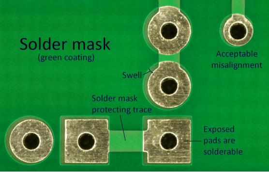
A solder-mask tolerance identifies the measured object: CAD opening, expansion, produced registration, remaining web, coverage, or thickness. Surface-finish thickness and legend printability have separate controls. One generic designation of “mask tolerance” cannot simultaneously define pad encroachment, dam width, and copper coverage.
Solder Mask Geometry
Expansion refers to the CAD opening relative to the pad. Registration refers to the produced mask edge relative to copper. The web is the mask material remaining between adjacent openings, while coverage is the mask material retained over copper. The 0.04 mm value refers to the minimum CAD expansion around a pad; the produced opening still depends on pad size and registration.
| Feature | Capability / limit |
|---|---|
| CAD solder-mask expansion | 0.04 mm minimum |
| Mask-to-trace clearance | 0.05 mm |
| Minimum mask web | 0.075 mm |
| Mask thickness on copper trace | 10–18 μm |
| Mask thickness at copper edge | >10 μm |
| Mask dam by color | 3.5 mil green; 5 mil black/white; 4 mil other colors |
| Legend line width | 0.10–0.15 mm |
| Legend text height | 0.8–1.0 mm |
| Legend-to-pad clearance | >6 mil (>0.15 mm) |
Separate pad openings, produced-registration measurements, and remaining-web measurements are used for fine-pitch and BGA pads. For example, if there is a physical dam separating adjacent pads, the mask-dam values may be color-dependent when assessing these pads. If there is no dam in the design, it must not be assessed against the same web value.
Surface Finish Thickness
All surface finishes are formed from process-specific layers that are separate from outline or copper-geometry tolerances. SUGA can quote: HASL: Thickness range is 2–40 μm. ENIG: Nickel thickness is 3–6 μm; gold thickness is 0.05–0.10 μm. ENEPIG: A 0.05–0.15 μm palladium layer is placed between nickel and gold.
If the drawing references IPC-4552B or IPC-4556A, the specified deposit system and measurement rule govern the order rather than the general capability range.
Legend Pad Clearance
Legend readability is determined by line width, text height, printing method, and pad clearance. Optical inspection can confirm the legibility of the characters and verify that the ink has not contacted the solderable pads. Surface-finish thickness must be assessed separately; a readable legend cannot confirm surface-finish coverage.
Controlled Impedance Tolerance and TDR Verification
PCB impedance tolerance identifies the intended target, line type, layer, material system, stackup, and TDR method. Acceptance results from a combination of the produced geometry, material system, stackup, and TDR result.
| Control or target | Tolerance / example | Construction condition | Verification output |
|---|---|---|---|
| Standard control | ±10% | Approved material + stackup + line type + target | TDR coupon / report |
| Tight control | ±5% | Narrower dielectric + copper + geometry control | TDR coupon + stackup + lot report |
| Single-ended target | 50 Ω ±10% | Design-specific target | Production-layer coupon |
| Differential target | 90 Ω or 100 Ω ±10% | Pair geometry + reference plane | Differential TDR trace |
| Tight differential target | Design target ±5% | Defined high-speed or RF construction | TDR result with agreed band |
What Controls PCB Impedance?
PCB impedance is influenced by dielectric thickness, material dielectric constant (Dk), copper thickness, reference-plane distance, line type, trace geometry, plating, and solder-mask condition. As such, compensation for PCB impedance is assigned based on the complete stackup, finished conductor geometry, and production coupon.
Etching Effects on Impedance
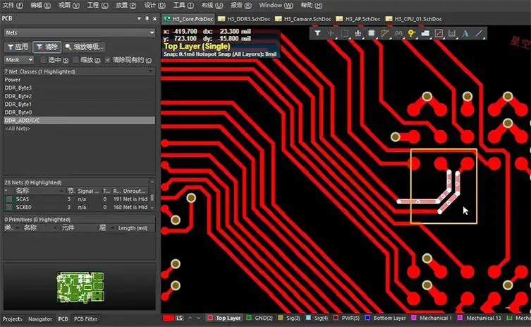
Etching affects the top width, bottom width, and sidewall profile of a trace. Outer-layer pattern plating can also affect the thickness and geometry of a trace. Therefore, artwork compensation must be consistent with the selected copper weight and process to ensure that the finished trace profile meets the required impedance target.
TDR Acceptance Bands
A production coupon represents the physical layer structure of the PCB and the critical geometry used for measuring PCB impedance. A TDR report includes the target, line type, coupon structure or location, measured result, acceptance band, test method, lot number, and acceptance status. TDR measures PCB impedance, while continuity and isolation tests identify PCB shorts and opens. If the production panel has uneven copper density or the distance between the coupon and production traces is significant, the coupon location and stackup revision must remain traceable to the finished boards.
PCB Manufacturing Tolerance Applications

Enclosure-Fit Control Boards
PCB enclosure fit is determined by mounting holes, cutouts, connector edges, board thickness, bevels, and fixed datums. A common issue is tolerance accumulation: each individual dimension may pass inspection while a connector edge and mounting-hole pattern drift in opposite directions because they were measured from different reference points. Using one functional datum and true position for housing-critical profiles, holes, and connector locations prevents chain dimensions from concealing fit errors. It also allows profile, NPTH, and copper-to-edge limits to be tightened locally while unrelated electrical features remain within standard capability.
Compact HDI Electronics
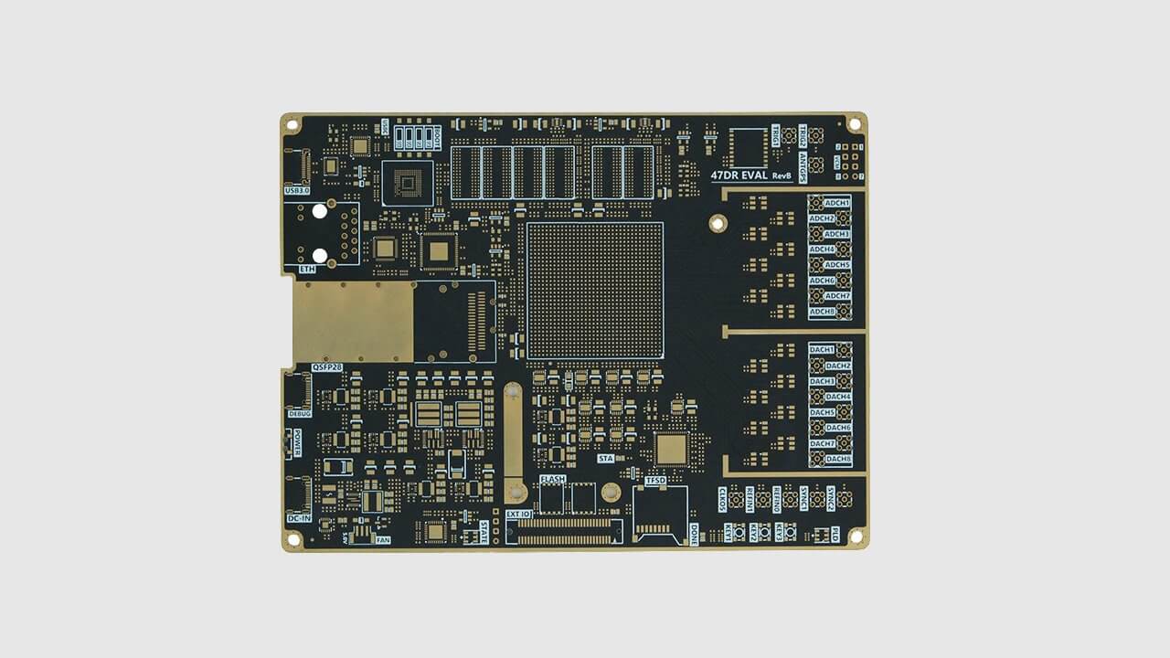
The design of thin HDI boards depends on coordinated microvia diameter, dimple, capture-pad size, dielectric depth, registration, fine trace and spacing, mask web, and finished thickness. A microvia diameter can pass independently, while reduced dielectric depth or layer shift reduces capture at the target pad, which may not be detected until microsectioning. The accepted construction links the laser process, sequential lamination, capture geometry, and microsection location as one record instead of separate pass or fail checks. This link prevents breakout, mask encroachment, and unstable stacked structures.
High-Speed and RF Boards
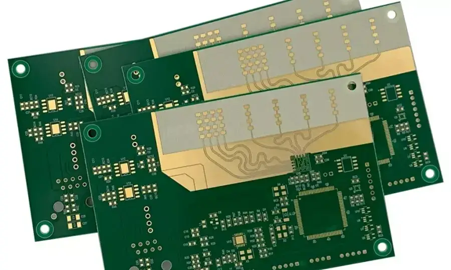
High-speed and RF boards rely on dielectric thickness, Dk, copper profile, trace geometry, reference-plane distance, and via transitions to maintain the targeted impedance. A trace may pass its impedance tolerance but still fail insertion-loss, return-loss, or skew requirements because these also depend on copper roughness, glass-weave orientation, and via-stub length. Boards with tight timing or multi-gigabit channels need these parameters stated separately rather than assumed to follow from a passing TDR result.
Traceable High-Reliability Boards
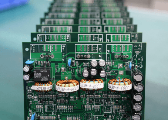
High-reliability boards pair each function-critical feature with its acceptance limit and inspection method. The risk is an inspection report that cannot be linked to the actual lot, coupon, or cross-section location. Controlled hole geometry, registration, dielectric spacing, flatness, and impedance should therefore include the drawing revision, sampling rule, inspection location, and lot identity needed to investigate production drift. These records should support review across repeated production, not only at initial acceptance.

Flex Connector Interfaces
Flex and rigid-flex connector areas use local stiffeners, gold fingers, ZIF contacts, coverlay openings, and rigid-to-flex transitions. The critical thickness is local rather than the average across the flex. A ZIF tail can meet the overall flex thickness but still fail insertion when the adhesive, coverlay, or stiffener stackup changes at the contact area. A separate measurement point should therefore be specified at the connector zone, together with controls for opening registration, outline, conductor exposure, and transition stress.

High-Current Power Boards
Power boards using 2–6 oz or heavier copper need wider geometry and spacing allowances than thin-copper designs. Heavy copper changes the etch sidewall angle, pad and annular geometry, hole-wall plating, mask coverage over raised copper topography, and local edge clearance. A narrow feature that is manufacturable at 1 oz may require local relief, a different copper process, or a larger mask opening when combined with heavy copper.
How Are PCB Manufacturing Tolerances Measured?
PCB tolerance inspection must match the feature, finished condition, and acceptance limit. Each result remains linked to the applicable drawing or stackup revision and manufacturing lot.
| Measured feature | Required drawing input | Inspection method and output |
|---|---|---|
| Finished board thickness | Stackup + finished-state definition | Micrometer or thickness gauge at defined locations; Dimensional report |
| Routed or laser profile | Datum + profile-method definition | CMM or optical profile measurement; First-article / final dimensional report |
| Routed slot / cutout | Finished width + datum + wall condition | Pin gauge, CMM, or optical profile measurement; First-article / dimensional report |
| Bow and twist | Construction + panel-balance assessment | Agreed flatness measurement; Flatness report |
| Finished PTH / NPTH | Tool + finished-hole definition | Pin gauge or optical hole measurement; Hole inspection report |
| Hole-wall copper / internal plating | Board-class requirement + plating plan | Microsection; Microsection / plating report |
| Annular ring / registration | Pad capture + compensation assessment | Optical inspection or microsection; Registration report |
| Trace width / spacing | Layer + copper weight + compensation assessment | AOI, coupon, or cross-section; Geometry report |
| Solder-mask registration / web | Opening + pad-pitch assessment | Optical measurement; Mask inspection report |
| Surface-finish thickness | Finish + layer-system definition | XRF or process-specific method; Finish measurement report |
| Controlled impedance | Target + stackup + line type + coupon definition | TDR; TDR trace / report |
PCB Fabrication Files
A PCB tolerance evaluation relies on the combination of the fabrication drawing, Gerber or ODB++ data, drill table, stackup, copper and solder-mask details, profile dimensions, and controlled-impedance specifications. Function-critical dimensions establish the desired finished state, datum, and inspection method.
Using this data, SUGA assigns every requirement to a standard, tight, or specialist production method and defines the manufacturing controls, inspection technique, and acceptance record to use for quotation and production.
To ensure the fabrication drawing, Gerber or ODB++ data, drill definitions, and stackup are all aligned to the same design revision, the CAM review should check that copper, mask, drill, and profile objects are aligned and manufacturable, as any discrepancy can influence the assigned production method or inspection method.
When plated and non-plated holes, slots, and routed cutouts occur together in an area, the drill table and drawing notes must separately identify each finished feature and wall condition, so the routing or drill file cannot silently override the intended plating state.
Which Standards Govern PCB Tolerances?
The approved drawing and applicable board specifications establish PCB tolerances for manufacturing purposes. IPC-6012F, IPC-6013E, and IPC-6018D cover rigid, flexible or rigid-flex, and high-frequency printed boards, respectively. IPC-A-600M is an aid for visual acceptability determinations. IPC-4552B and IPC-4556A apply to ENIG and ENEPIG deposit systems when specified as finishes. The TDR method used to measure characteristic impedance is provided in IPC-TM-650 2.5.5.7.
Quality-system or material compliance does not negate feature-specific acceptance. The purchase order will still identify the drawing revision number, IPC class, finish specification, sampling rule, and acceptance record required to fulfill the order.
Our PCBA Production Lines
















PCB Manufacturing Tolerances FAQ
Confirm at quotation, rather than afterward, which production and inspection methods will be used, since jobs processed at partner factories can use different coupon or microsection methods from SUGA-managed jobs under the same capability category.
Use true position if the holes or connectors need to relate to a functional datum system instead of referencing independent horizontal and vertical dimensions. When using separate tolerances on the X and Y dimensions, you can mask accumulated error when each dimension is referenced from a different origin point. It is important that the drawing indicates all datum features and the relevant material condition, as well as the gauge or CMM method used to verify compliance.
Ask the supplier to provide the coupon's panel position and stackup revision information alongside your particular product traces, rather than just a passing TDR number. Without that connection, a passing coupon report only shows that the process was capable somewhere on the panel, not necessarily that the specific traces you are interested in were measured.
Not automatically. The general tolerances found in a title block are intended for routine dimensions. However, connector edges, mating slots, press-fit holes, and enclosure datums should generally have feature-specific callouts. State the finished condition, nominal value, tolerance direction, datum, and inspection method beside the critical features so that a broad default tolerance is not applied to the functional requirement.
Instead of a single flex-thickness callout, specify where the measurement is taken. For example, measure the flex thickness at the ZIF contact area, including adhesive and coverlay, rather than using only a flex-thickness value without a defined location. A supplier measuring flex thickness at its own selected measurement point could still report compliance without checking the connector-critical zone.
Yes. The imaging processes for copper and solder mask are performed separately; thus, the edge of the mask may shift relative to the copper pad. The fabrication drawing should indicate the pad size, CAD opening, mask expansion, registration tolerance, and required remaining web. Optical inspection of the completed product measures the finished mask-to-copper relationship against these callouts.
Several items can affect confirmation of the quoted tolerances: layer count, board thickness, copper weight, panel size, and measurement datum. Keep these items on a standing checklist so that when any of them changes, reconfirmation is required before production, even if the PCB drawing revision number has not changed.
Zero tolerance does not exist in physical manufacturing or measurement processes. A design intent that allows no variation must be translated into a measurable acceptance band with defined units, datum reference points, finished state, and inspection method before acceptance of the manufactured PCB.