Upload BOM & Gerber


Contents
show
What Is a 4 Layer PCB?
A four-layer PCB consists of four conductive copper layers with insulation between each layer. Solder mask protects exposed circuitry, while silkscreen carries markings. Neither these layers nor the CAD mechanical layers count toward the four copper layers on the PCB. The designation of a four-layer PCB does not assign a specific signal, ground, or power configuration; a published specification from a four-layer service is just one example of that distinction.
Copper Layers, Core, and Prepreg
A four-layer PCB has 4 copper layers, with a core dielectric and prepreg providing insulation between the copper layers. In a traditional rigid core/foil construction, the stack is L1 copper / prepreg / L2 copper / core dielectric / L3 copper / prepreg / L4 copper. Therefore, the structure contains 4 copper layers separated by 3 insulating regions. Each prepreg region may contain several sheets that, when laminated together, form the insulation between the copper layers.
The core layer is made with already-cured insulation that has copper on both sides. In a traditional four-layer PCB build-up process, prepreg is made of partially cured resin that flows and cures during lamination, bonding the core layer to the outer copper foil layers.
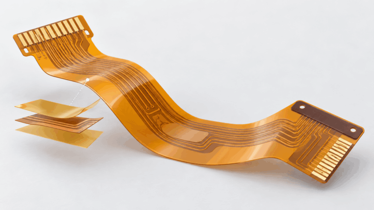
Rigid, Flexible, and Rigid-Flex describe the mechanical construction, while the four-layer designation refers to the total number of copper layers in the PCB. Several factors determine the ability of the PCB to bend and be flexed repeatedly, with flex-to-install design guidance being a common example. An optional design consideration for a 4-layer PCB is the use of either blind or buried vias.
During the manufacturing process, the fabricator will create the inner copper layers, etch them, and inspect them before the layers are laminated together. The next steps in the process are drilling holes, metallizing and plating the hole walls, and forming the outer conductive copper layers. Once an inner trace is buried after lamination, that trace cannot be modified or accessed directly. Depending on whether the PCB has blind or buried via structures, the manufacturing sequence will change because these interconnections must be formed at the appropriate stage before later layers close the structure.
When Is a 4 Layer PCB the Right Choice?
A 4-layer PCB is a good choice if a 2-layer layout will not accommodate the necessary routing, continuous reference planes, and power paths.

Let’s say that there is a theoretical compact circuit board that has connectors at multiple locations on the bottom of the board, which cross over the ground copper needed under the most critical traces in an application. By moving the ground reference to an inner layer, that problem can be resolved.
When there are other requirements such as BGAs, there may still be too many usable channels being consumed by dense components. A good way to identify how to route the critical signals in a six-layer stackup is to draw out a proposed six-layer stackup and identify the necessary connections.
Selecting between several “high frequency” interface designations or clock frequencies is not sufficient to find a solution. The characteristics of the signal edges, the total path lengths, and the continuity of the ground references determine the behavior of the interconnects used in a particular solution; any labelling of a frequency does not specify any of the above-mentioned characteristics.
For example, the ESP32 Hardware Design Guidelines do recommend that boards using this processor should use four layers; but in addition, the guidelines allow for two-layer designs that meet specific ground layout requirements.
Additionally, the allowance applies to the stated device and layout conditions, while the signal integrity and certification of other radios using the board would still depend on that board’s own layout and RF conditions.
Which 4-Layer Stackup Should You Use?
First, determine the layer assignments based on the critical signal references and what is needed for power distribution. In this case, “SIG” represents signal routing; “GND” represents ground copper; and “PWR” represents power copper. The actual coupling to the adjacent references depends on the dielectric spacing.

An electronic design should show the most critical net on its intended layer and track the adjacent copper network to the device or receiver. Using the stackup as a starting point allows the appropriate routing and reference requirements to be checked against the final layout, since no single stackup fits every placement, routing, and reference requirement.
Power on a Plane or on the Outer Layers
Multiple supply power rails can use traces or local copper where space, load positions, and current paths permit, so a dedicated power plane is not always required. When two inner ground layers are used, one can carry digital return current and the other analog or RF return current, keeping the return-current domains separate. Whichever plane carries the lighter current density may have room to accommodate additional supply routing without overcrowding the outer layers. A power layer split among multiple supply rails, however, may disrupt the reference for traces routed beneath the bottom side of the board.
The outer ground pour should be connected to the intended ground network while maintaining the required clearance around critical traces routed through the outer layer.
In some cases, inner-signal and outer-ground arrangements can also be used. The reference distance, component-pad access, and escape routing through the outer copper should be checked.
Board Thickness, Copper, and Impedance Geometry
Finished board thickness differs from trace-to-reference spacing. Two boards with a common overall thickness can differ in their outer dielectric heights, copper conductor thicknesses, and transmission-line geometry.

Read the Actual Layer Spacing
The following fields come from a published four-layer service specification.
The document also has an alternate construction, so confirm the stackup for the actual order. The finished dielectric spacing should be modelled, not the overall 1.6 mm thickness. The rounded nominal fields should not be summed as an exact total.
Set Geometry from the Interface and the Stackup
Start with the impedance target and impedance tolerance of the interface or device. Next, set up the transmission-line configuration, reference spacing, copper thickness, and material properties before calculating trace width. Differential geometry also involves pair spacing and coupling, while controlled impedance follows the same geometry-first method.
The term “FR4” does not contain a design Dk. The proper application of Dk is dependent on the material grade, build-up method, operating frequency, and method of measurement that match your intended calculation; loss-sensitive path calculations require appropriate loss data too. When changing suppliers or stackups, you must check all of these inputs again even when the board is still nominally 1.6 mm.
Check the Copper, Holes, and Thermal Path
The drill diameter and the finished hole diameter after plating should be differentiated. For the thickness-to-drill aspect ratio, confirm which diameter and thickness convention the manufacturer uses. All four items must be checked together: copper thickness, annular ring, inner-layer clearance, and hole process. The published rules for the four-layer construction explain the service-specific acceptable combination.
Trace width and copper thickness affect the current path under its allowed temperature-rise conditions. Review the entire length of the route, including narrow sections, rather than assigning copper weight based entirely on current. Heavier copper also affects feasible fine-line geometry.
Mechanical balance considers the thicknesses of the dielectric and copper as well as the distribution of copper. Just because you change the names of PWR and GND does not change the way it’s built, and how much warpage the board experiences will still depend on the actual copper distribution and the dielectric thicknesses on each layer, regardless of how the materials are labeled or what they are called. The multilayer fabrication guidelines treat both lay-up and bonding as construction processes, not as electrical labeling processes.
Look at the path that goes from the package to the pad, copper, and thermal vias. The pad and via layout requirements are connected to the assembly requirements based on ESP32 EPAD guidance. The temperature reduction comes from that pad-copper-via path along with the specific dissipation and soldering conditions of the device, not from the multilayer count alone.
How Do You Route Signals on a 4-Layer PCB?
Always trace out all critical signals with the associated continuous reference before making any layer transitions, as the high-frequency return current will take impedance-dependent paths, and any split or void in the reference will force it to take a detour, enlarging the loop.

Follow the Return Path Through a Layer Change
Connect the L1 driver to the L4 receiver through a signal via; use SIG/GND/GND/SIG, and make sure both grounds are part of the same network, without isolation boundaries.
- Locate Your References. The L1 segment sits beside the L2 ground, and the L4 segment sits beside the L3 ground. Make sure to check both routes for connector and via clearances.
- Find Interruptions. Any crossing over a reference split will force the return path around that opening. You may need to reroute over continuous copper or consider repartitioning. It is not necessary to cut the ground plane to create separation between analog and digital electrical functions.
- Inspect the Ground Transition. Place a ground stitching via near the signal transition to connect the two references that are part of the same net. Inspect the location and geometry of this via to make sure this connection is adequate.
- Change L3 to Power. With the SIG/GND/PWR/SIG configuration, the bottom segment now sits beside a different network. You should never short that power plane using a ground stitching via. You should prefer a continuous ground reference where applicable. If you are unable to maintain a continuous ground reference, then you must reassess the power distribution network, decoupling, and transition geometry.
Inspecting reference transitions this way is in accordance with the interface layout guidelines; other-net transitions should still undergo circuit-specific analysis, as opposed to being dictated by a universal via distance or capacitor prescription, and all required isolation boundaries should remain intact.
Which Copper Layers Does a Through Via Connect?
The electrical connections of a through via depend on the copper attached to its plated barrel because the copper creates the electrical connection to the barrel. For example, a signal that connects L1 to L4 may have clearance openings, or antipads, in L2 and L3 around the barrel, but the barrel passes through these openings without electrical contact.
A ground via can provide a direct connection from the outer ground pad to the inner ground plane using a standard through via. If there is a need for denser interconnection than what is available through standard through vias, a blind via becomes an option. Microvias, buried vias, and blind vias are options for creating dense interconnections in a PCB, while backdrilling can be used to remove unwanted barrel stubs; via-in-pad construction decisions involve pad geometry and assembly considerations. Each of these methods has distinct construction requirements, and the specific characteristics must be verified with the PCB fabricator before committing to the structure.
For bottom-side decoupling capacitors, it is best to follow a loop that consists of the power supply pin, capacitor, and ground connection. When working with decoupling capacitors, all three of these connections, as well as the traces and vias connecting them, must be checked. The capacitor value and placement should be selected according to the circuit and device requirements.
The differential pairs, length-matching rules, timing constraints, and routing constraints should correspond to the interface, edge behaviour, and timing budget. For example, if an existing board has been designed with a four-layer stackup, you should use the actual stackup and high-speed PCB layout guidance to convert allowable timing differences into routing constraints rather than borrowing a mismatch limit simply because another board also has four layers.
Where Four Layers Work Well and When They Do Not

Compact MCU and Wireless Controllers
Moving a continuous ground reference to an inner layer is advantageous for a small controller containing an MCU, radio, switching regulator, USB, and highly dense peripheral routing. The main advantage is that critical outer-layer traces can maintain a stable return path while power and lower-priority routing use separate space. Whether a properly disciplined two-layer layout will suffice for a particular RF design is determined by routing density, return-current paths, antenna placement, and the vendor’s layout requirements — not the existence of RF alone.
Mixed-Signal Sensor and Control Boards
Control and sensor boards are generally composed of low-level analog sensing, converters, digital control circuits, and switching power. Often an engineer can exhaust clean routing space long before reaching the raw connection count. Four-layer boards allow sensitive traces to remain over continuous reference copper while noisy current loops and power paths are kept physically compact. Validate the actual return paths before splitting the ground: maintain the necessary isolation boundaries and route to keep analog and switching currents from sharing avoidable loop areas rather than splitting the ground by default.
USB and Ethernet Embedded Systems
When dealing with USB, Ethernet, and similar edge-rate-sensitive interfaces, using a four-layer PCB can make controlled impedance and continuous references easier to achieve because the PCB stackup determines the trace-to-plane geometry rather than the total PCB thickness.
To maintain signal integrity with any layer count, considerations such as pair geometry, via transitions, reference changes, connector footprint design, and stubs still need to be considered.
When multiple interfaces compete for the same escape channels or force reference changes, using a six-layer allocation could be more effective than routing dense detours through four layers.
Dense QFN and BGA Control Boards
When implementing fine-pitch QFN and BGA packages, a PCB design choice will often come down to escape routing from the package. If the escape routing can be completed without cutting critical reference copper, a four-layer PCB may be sufficient. This is also typically true if practical routes are still available for power distribution.
However, if connector fan-out, BGA escape, multiple high-speed buses, and power distribution consume the same routing channels, moving to six layers may allow for a cleaner layout than forcing repeated detours.
Checking a Four-Layer Design Before Fabrication
To confirm the design requirements are correct, send the fabricator a current and consistent revision of the drill and outline data alongside these fabrication requirements:
- Confirm all four copper layers, their order, reference networks, and via connections.
- Match the material, copper thickness, dielectric spacing, hole dimensions, and clearances to the intended construction. A design-rule check validates configured rules but does not confirm that all manufacturing and functional requirements have been met.
- Identify controlled-impedance nets or structures, targets, and tolerances. Include a BOM and component placement data when the work includes assembly.
AOI is one of several methods used to inspect copper patterns. Bare-board electrical testing checks connectivity for opens and shorts. TDR is a common method used to measure representative impedance structures, often on a coupon that must correspond to the relevant board construction, as described in controlled-impedance guidance. These checks do not validate assembled functionality or EMC of the system.
Surface finishes and platings depend on solderability, flatness, contact use, and how the assemblies will be stored. To make a price comparison, variables such as board area, quantity of boards, material, copper, hole process, finish, testing, and delivery conditions must be consistent because layer count is not the only variable driving PCB price differences.
References & Sources
- 4 Layer Prototype Service – OSH Park
- PCB Multi-layer Fabrication – Lay-up and Bond – Eurocircuits
- Designing flex-to-install PCBs – Eurocircuits
- High-Speed Layout Guidelines – TI
- PCB Layout Design – Espressif
- The Right Way to Use Power Planes in a 4-Layer PCB Stackup – Altium
- What is controlled impedance? – Polar Instruments
- Blind and Buried Vias – Eurocircuits
- What Are the Basic Guidelines for Layout Design of Mixed-Signal PCBs? – ADI
- High-Speed Interface Layout Guidelines – TI
- During Production – Eurocircuits