Upload BOM & Gerber

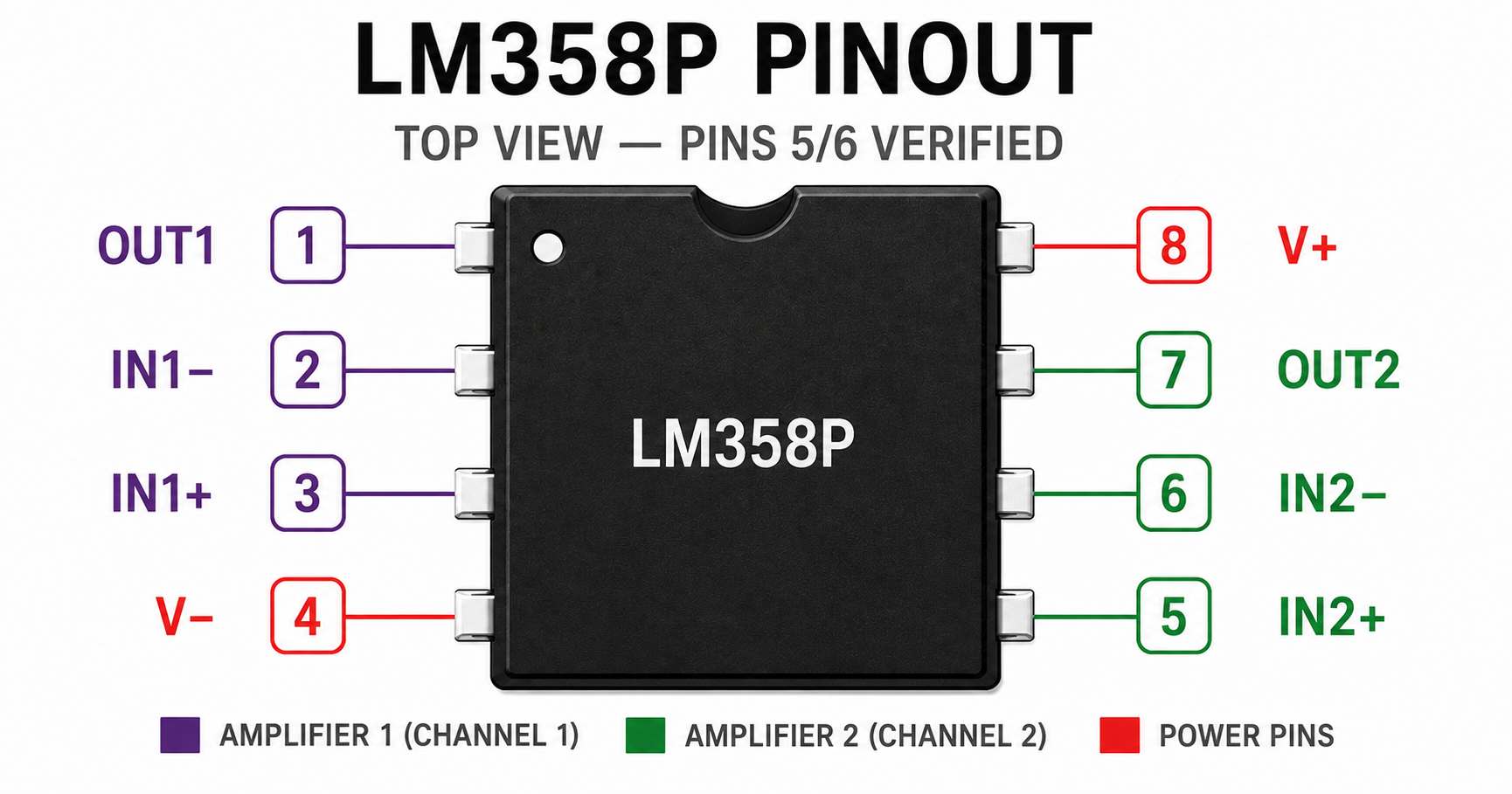
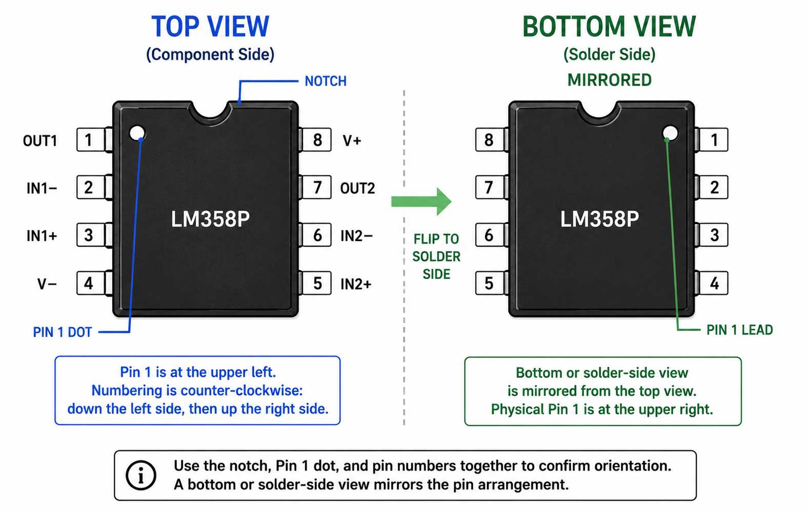
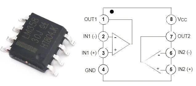
the pin arrangement for the Texas Instruments LM358P in the PDIP-8 package, as seen from the top: Pin 1 is OUT1, Pin 2 is IN1−, Pin 3 is IN1+, Pin 4 is V−, Pin 5 is IN2+, Pin 6 is IN2−, Pin 7 is OUT2, and Pin 8 is V+. Confirm the manufacturer and the package view. Then carry those pin numbers through the schematic symbol, footprint pads, and assembly orientation.
The TI LM358P is a two-op-amp device in an eight-pin through-hole package. The pinout, although simple, does have errors that could be easily overlooked in the course of a brief glance; these include mistaking the bottom view for the top view, transposing pins 5 and 6, and using specifications for the newer LM358B/BA for the older LM358P.
Contents
show
How Do You Identify the Exact LM358P?
Begin with the manufacturer, complete marking or order code, and package information. The TI datasheet describes the LM358P as the legacy LM358 device package option in an 8-pin PDIP, with an operating temperature rating of 0°C to 70°C (TI LM358P Product Page). The "P" suffix is related to TI's order code, rather than a universal name associated with the PDIP package type.
This distinction matters, as the LM358 part name is widespread and includes many different manufacturers. Onsemi uses the designation "LM358NG" for a PDIP package option, whereas ST uses "LM358PT" for a TSSOP-8 part number (Onsemi LM358 datasheet; ST LM358 datasheet). The use of different suffixes among manufacturers makes it easy to select the wrong package before routing any pins.
The TI datasheet indicates that the LM358P is the "legacy" device and provides separate listings for LM358B and LM358BA. While all three devices are included in the same datasheet, they differ in performance and supply limitations. Record the exact orderable part in the BOM and bind the schematic and footprint to that record. A generic label in the library is not sufficient to prove the actual part.
Read the LM358P Pinout from the Top View
With the pinout viewed from the component side with the notch facing upwards, pin numbering runs counter-clockwise. Starting from pin 1 (the upper left corner), the pin numbering proceeds downward on the left side, beginning at pin 1, until reaching pin 4 (the lower left corner), and then continues back up to pin 8 (the upper right corner). TI has explicitly described the LM358P package pinout diagram as being viewed from the top.
The solder-side view (bottom) is mirrored relative to the top view and can still look plausible while placing each physical lead on the opposite side. When using a PCB footprint editor, the display may depict the PCB in one of three possible ways (top, bottom, flipped layer). Do not assume that the left and right sides will correspond to the same positions on the bottom side. Always refer to the Pin 1 pad indicator, notch location, and the numbered diagram for guidance when determining pin orientation.
Which Pins Belong to Each Op-Amp Channel?
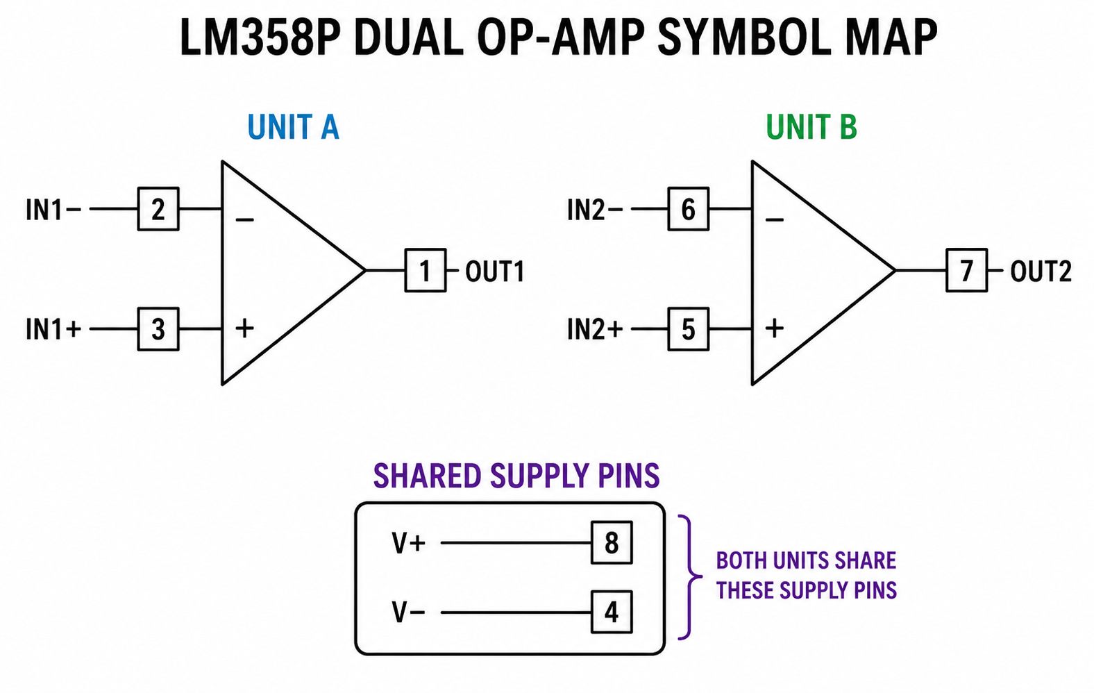
It's relatively easy to reverse the order when wiring channel 2, as its functional order runs 7-6-5 rather than 5-6-7.
According to TI Table 4-1, pin 5 is assigned to IN2+ and pin 6 to IN2−. If the image you are using shows different pin assignments than TI's table, please use TI's table as your reference. This single verification helps prevent your negative-feedback circuits from becoming positive-feedback circuits.
What Do V+ and V− Mean in Single- and Dual-Supply Circuits?
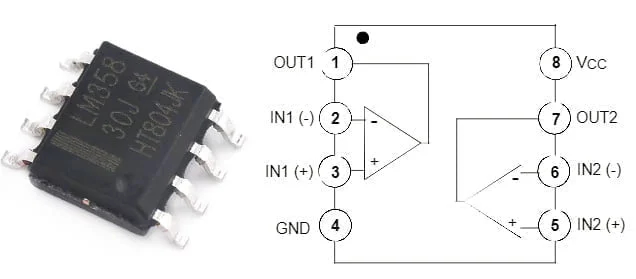
V+ (pin 8) is the highest power supply rail, while V− (pin 4) is the lowest supply rail. In a single-supply circuit, V− is usually connected to ground (or 0 V). In a dual-supply circuit, V− is connected to the negative rail. The negative sign (−) in V− does not make it an inverting input signal.
TI recommends an overall supply range of 3 V to 30 V for the legacy LM358. Therefore, for a 5 V single supply, V+ would equal 5 V and V− would equal 0 V; for a ±12 V supply, it would create a 24 V overall supply range.
For PCB layout design, TI recommends using 0.1-µF bypass capacitors between the supply pins and ground, placed as close to the device as possible. In a single-supply circuit, the V+ pin would need to be bypassed with one capacitor to ground. (See the TI LM358 datasheet.)
The signal voltage level and datasheet specification limits are defined in relation to the V+ and V− rails rather than only relative to ground. When the reference voltage system is unknown, it is essential to distinguish GND, 0 V, and the negative supply before concluding the input or output voltage level.
Correct Pins Can Still Produce the Wrong Voltage
A pin map that has been assembled correctly does not guarantee that the input signal will be within the common-mode range or that the output voltage will reach the requested voltage. For example, the input voltage range for the legacy TI LM358 extends from the negative supply to below the V+ rail. The output-high voltage limit is determined by the power supply, load, and temperature (see TI's LM358 datasheet for details).
Keep all three categories of data separate from one another. The Absolute Maximum Ratings state the limits beyond which damage may occur to the device, the Recommended Conditions state how the device should be used, while the Electrical Characteristics indicate how the device will perform when tested under specific conditions. None of the categories can replace or substitute for any of the other two.
TI's LM358B/BA devices have increased the recommended power supply to 36 V and specified approximately 1.2 MHz GBW. However, these specifications do not improve the performance of an LM358P. Also, the higher the output load, the more likely the high-side output will decrease due to the increased load. Refer to the exact device row to determine the actual operating point, not the family headline.
How Do You Verify the Symbol, Footprint, and Package View?
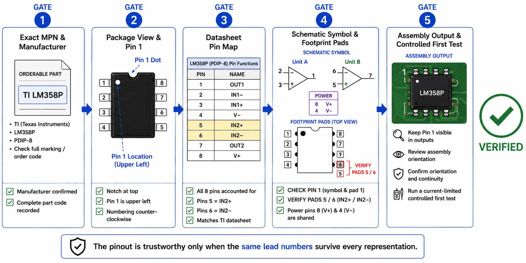
For a given orderable part, the same physical lead numbers must be preserved across five separate representations: the orderable part, package view, datasheet pin table, schematic symbol, and footprint or assembly output. This means that an apparently correct-looking symbol can still connect to the wrong copper if the pin designators associated with the symbol do not correspond to the footprint pads.
While Altium provides components with multiple graphical parts, KiCad allows for multi-unit symbols; in KiCad, the letter of the unit that is visible does not replace the electrical designation of the pins (Altium Symbol Documentation; KiCad Schematic Editor). Review the actual object in the library along with any separate power unit.
After running ERC and DRC, review the 3D and assembly views of Pin 1, its rotation, as well as pads 5 and 6. These tools verify different types of errors; in isolation, no tool confirms the validity of the entire connection chain.
How Do You Run a Controlled First Test?
With the power off, confirm the orientation and pin continuity first. Then, using a current-limited power supply, test one of the channels as a voltage follower by tying the output to the inverting input with a properly biased non-inverting signal well within the common-mode range and using a light load on the output. Measure both supply pins to determine if they are supplying power properly before judging whether the output has followed the input.
Instead of starting near 5 V for a 5 V single-supply application, begin with either a 1 V or 2 V input signal as a follower input. The lower-level voltage signals allow for significant common-mode and output headroom to complete a basic check of the circuit. If the output follows the lower-level signal properly, but as the input signal approaches the upper rail begins to clip or fall off, then the limits of operation are determined by the input and output levels rather than a misapplication of the pinout. If the lower-level test fails, check the package view and pins 5 and 6 to ensure the correct package configuration. After that, confirm the supply polarity, check the load, and finally ensure the manufacturer part number matches.
Also ensure that an unused amplifier is in a defined stable linear circuit with valid common-mode inputs and feedback because TI recommends that floating inputs can create erratic output conditions and that tying the inputs to low-impedance power rails may violate the input conditions (TI Application Report SLOA277B). Use this report to guide the power supply and device generation.
The bench operation sequence is intended to supplement a practical setup guide and cannot be interpreted as the authoritative reference to the exact TI pinout or guaranteed limits. Expand the bench test to document the functional testing of the PCB using established stimuli, limits, loads, fixtures, and traceable results.
Common LM358P Applications and First Checks
The same pinout of the LM358P applies to numerous common circuits, but each configuration reaches a different electrical limit first.
Comparator, Bandwidth, and Substitution Boundaries
While switching may be familiar from comparators, an op amp is not necessarily the best choice for applications where comparator functionality is required, because phase reversal due to common-mode violations, overload recovery restrictions, and a 0.3 V/µs slew rate can inhibit switching functionality. For predictable saturation recovery, threshold response, and output interfacing, a comparator should be used.
Frequency of operation is not fixed for the LM358P. Gain in closed-loop reduces the available bandwidth, while the slew rate and amplitude of an input signal create a limit to the maximum large-signal performance of the LM358P; a 0.7 MHz GBW does not guarantee full-scale waveform performance at 0.7 MHz.
For example: An active non-inverting configuration on a 12 V single supply, in the mid-rail region of the supply voltage, will use a 10 kΩ reference resistor plus a 100 kΩ feedback resistor (OUT to IN-) to achieve a gain of 11. A 100 mVpp input signal will require a 1.1 Vpp output signal; both are well within the allowable swing of the amplifier's output over a 12 V rail. The closed-loop bandwidth will be calculated from GBW ÷ gain, i.e. 0.7 MHz ÷ 11 = 64 kHz, which serves as a ceiling to check before assuming that signals at faster rates can be tracked by the LM358P.
For the same single-pole RC filter at 1 kHz, this filter's cutoff frequency operates entirely within the limits established by the LM358P, so the GBW of 0.7 MHz provides three orders of magnitude of margin, and the slew rate becomes limiting at approximately 95 kHz (assuming a 1 Vpp swing, slew rate ÷ (2π × peak voltage)). Therefore, as frequency approaches tens of kHz at large swings, the slew rate may become the limiting factor before the feedback network.
As the shunt voltage in low-side sensing is generally near ground, the offset voltage of the LM358P could have a significant impact on the measurement accuracy, especially if the shunt drop is only a few mV. The offset error must be calculated prior to making any assumptions regarding the accuracy of the measurement; when close attention must be paid to the measurement error, current-sensing amplifiers may be better suited.
The matching eight-pin layout does not mean the two parts are drop-in compatible. Always compare the new replacement device datasheet with the old part's operating point before performing a BOM change.
Verify the Number Chain Before Release
Verify one consistent number chain from the TI order code and the top-view drawing all the way through the symbol designators, footprint pads, assembly orientation, and intended operating point.
References & Sources
- LM358P – Texas Instruments
- Industry-Standard Dual Operational Amplifiers datasheet (Rev. AB) – Texas Instruments
- Application Design Guidelines for LM324 and LM358 Devices (Rev. B) – Texas Instruments
- LM358, LM358A, LM2904, NCV2904 Single Supply Dual Operational Amplifiers – onsemi
- LM358 Low-Power Dual Operational Amplifiers – STMicroelectronics
- Creating a Schematic Symbol – Altium
- Schematic Editor 10.0 – KiCad