Upload BOM & Gerber

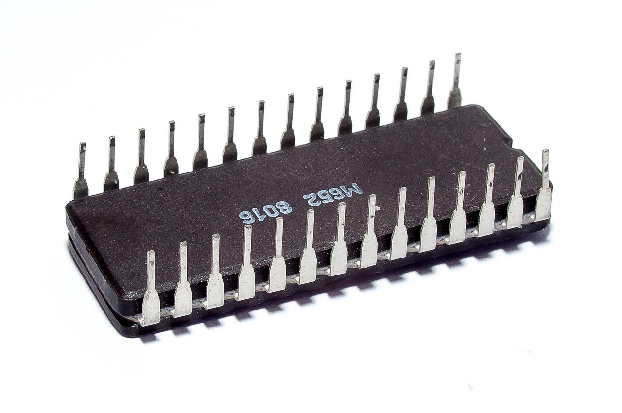
A DIP, short for Dual In-Line Package, is an electronic component packaging style consisting of two parallel rows of leads. Most DIP integrated circuits connect to printed circuit boards through through-hole mounting or plug into compatible sockets. The definition of DIP describes how the device is laid out; it does not define a single size or specify the entire through-hole assembly process.
DIP represents many different packaging styles. Some DIP packages may have the same number of pins and the same electrical function but vary in pin pitch, body width, row spacing, lead configuration, temperature grade, or pin assignment. Therefore, when determining how to replace a device or design a footprint, the complete manufacturer part number and associated package option must be obtained.
DIP stands for Dual In-Line Package. It specifies that the device has two parallel rows of leads but does not indicate the lead pitch, row spacing, body width, socket size, or PCB footprint. Verify the complete manufacturer part number, package suffix, pinout, Pin 1 orientation, and dimensional drawing before treating two DIP devices as interchangeable.
Contents
show
What Does Dual Inline Package Mean?
The term “Dual” refers to the two parallel rows of leads, while the term “In-Line” refers to the fact that the leads in each row are aligned in a straight line. An established alternative to DIP is DIL, an abbreviation for the same packaging arrangement; it does not designate a different electrical function.
DIP packaging and through-hole technology describe different levels of the hardware. A Dual In-Line Package (DIP) is a physical package in which an integrated circuit (IC) can be contained. Through-hole technology is used to mount and solder DIP ICs and many other leaded components, such as connectors, transformers, relays, switches, capacitors, and axial components. Although DIP ICs are generally assembled through holes, not all through-hole components are DIPs.
The circuit inside a package is not defined by the package name. For example, logic gates, op-amps, memory devices, microcontrollers, drivers, opto-isolators, resistor packs, and other functions are available in DIP-style packages. The electrical function of the device and the data needed to use it are derived from the device part number or datasheet; the DIP designation solely refers to the external physical arrangement.

What Is Inside a DIP Package?
A typical molded plastic DIP contains a semiconductor die that performs the electrical function, a die-attach area, a metal lead frame, fine wire bonds that connect pads on the die to the inner ends of the lead frame, an encapsulating body, and external leads that connect to the PCB or socket.
The lead frame serves both electrical and mechanical purposes. It supports the die during the packaging process, provides conductive pathways to the external circuit for electrical signals from the die, and acts as part of a thermal path to help dissipate heat from the die. The material, plating, cross-section, and internal structure of the lead frame depend on the package design and should not be assumed based solely on the external appearance of the package.
A plastic DIP package is commonly identified as a PDIP, while a ceramic DIP package may be identified as CDIP or CERDIP. Ceramic construction can support different mechanical, thermal, moisture, or reliability requirements, but those properties depend on the exact device grade and package specification.
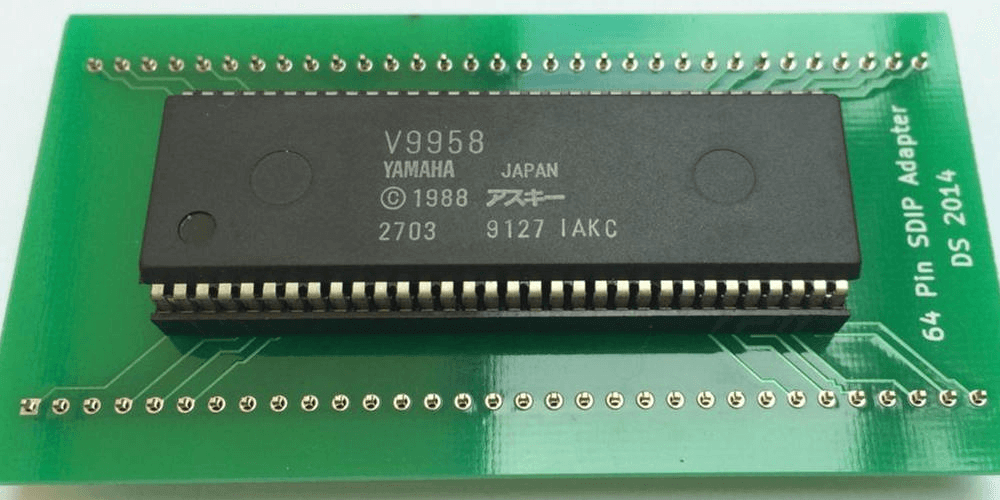
How Do You Recognize and Read a DIP Package?
Common characteristics of a conventional DIP integrated circuit package include a rectangular shape with two rows of leads along the length of the package and an orientation marking, such as a notch, dot, or molded symbol. The rectangular shape alone does not provide enough information; the orientation marking and package diagram establish the location of Pin 1 and the view orientation of the package.
For example, Texas Instruments provides a concrete 14-pin example for the CD74HC11 integrated circuit. In the stated top view, Pin 1 is the upper-left pin. Numbering continues down the left row to Pin 7, crosses the end of the package, and returns up the right row to Pin 14. This familiar counterclockwise pattern must still be confirmed against the actual datasheet because pin count, view direction, and orientation symbols vary by package and manufacturer.
The mechanical interface of the device is divided into six fields:
- Pin count: Refers to the total number of leads that are external to the package. This does not define pin compatibility or package width.
- Pin pitch: The distance between adjacent leads in the same row, measured from center to center.
- Row spacing: The distance across the two rows of leads at the reference points defined in the package drawing.
- Body width: The overall width of the plastic or ceramic body of the device, which is not the same as the lead-row spacing defined above.
- Lead geometry: Details related to lead width, thickness, length, bend, position tolerance, and seating relationship.
- Pin 1 orientation: The physical reference point for aligning the device with the appropriate electrical pinout and PCB numbering.
A typical full-size DIP package has a pitch of 0.100″ (2.54 mm), and shrink-DIP socket families also use a grid size of 0.070″ (1.778 mm). The lead-to-lead spacing may match the pitch but may not meet the row-spacing, body-clearance, or lead-size criteria for the compatible hardware.
DIP, DIL, PDIP, CERDIP, Skinny DIP, and Shrink DIP
Package abbreviations provide a shorter description, but these abbreviations do not denote the orderable part number or outline code. Mechanically incompatible packages may be offered within the same electrical device family. For example, Analog Devices lists variants of the AD586 in 8-lead PDIP, CERDIP, and SOIC, with a different package code for each.
What common DIP package terms identify
The terms “shrink” and “skinny” should not be defined as the same type of package, as these two definitions refer to different DIP dimensions. “Skinny” refers to a narrower DIP package in which the distance across the package or lead rows is reduced, while “shrink” refers to the lead spacing along a row, or the pitch between adjacent leads, being reduced. In some cases, both dimensions change within a package family, so the dimensional drawing of each package must be analyzed to determine which dimensional changes were made.
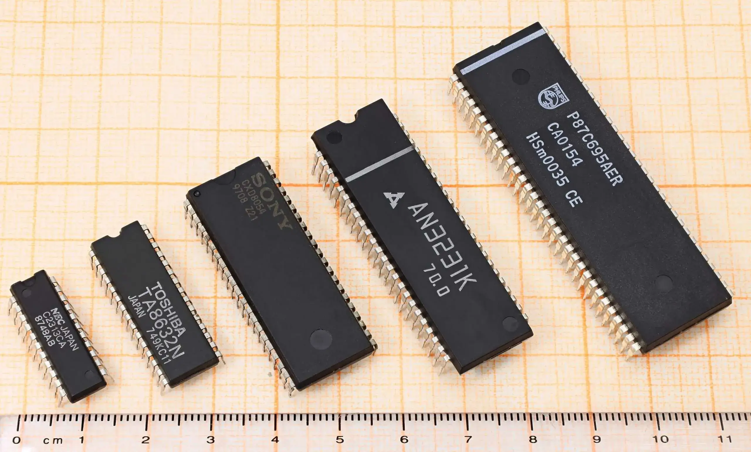
How Do You Check Whether a DIP Will Fit?
For a DIP package to be compatible, there must be agreement between the electrical device and the physical destination, specifically the DIP package and the PCB on which it will be installed. Although the DIP package name, shape, and lead count might be clues during the screening process, they should not be considered the final determination. To ensure compatibility, follow these steps:
- Make a record of the complete manufacturer part number of the DIP package, including any package suffix and temperature suffix.
- Locate the datasheet or package drawing for the exact orderable part number.
- Verify the electrical pinout, supply pins, no-connect pins, and any functional differences between the two DIP packages.
- Verify the drawing view, lead count, and Pin 1 location or orientation.
- Compare the pitch, row spacing, body width, lead size, lead length, and seating dimensions as separate limits.
- Compare the complete dimensional ranges with the socket drawing, breadboard dimensions, or PCB footprint.
Four different records must agree for a replacement DIP package to be approved. The schematic symbol indicates the electrical connections; the BOM record provides the official manufacturer code of the DIP package; the package drawing indicates the body, leads, tolerances, and orientation of the DIP package; and the PCB footprint indicates the holes, pads, numbering, assembly courtyard, and any clearances required for assembly. A matching symbol or matching pin count cannot substitute for the other three records.
Why Equal Pin Count and Pitch Are Not Enough
Having an equivalent pin count and pitch does not necessarily mean that a DIP package is compatible. For example, Microchip publishes both an 8-lead PA plastic DIP and an 8-lead JA ceramic DIP for the TC4420/TC4429 family with the same lead count and a 2.54 mm pin pitch. To determine compatibility, compare the body dimensions, overall row spacing, lead width, lead length, and height limits, as these specifications are not identical for both packages .
Device-specific package example: TC4420/TC4429 8-lead PA PDIP vs. JA CERDIP
An equal pin count and equal pitch match only two fields. The total min-to-max dimensional ranges of a part’s package must allow it to enter the target holes or contacts without interference. The hole-size relationship must allow the leads to enter the target holes or sockets without loose retention, lead deformation, incorrect insertion depth, or incorrect seating.
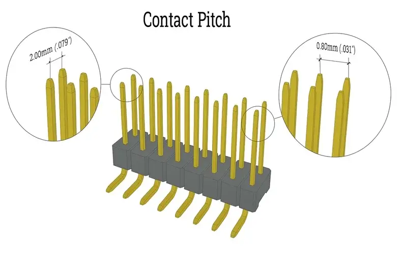
DIP Sockets, Breadboards, and PCB Footprints
Although one device may pass inspection for one destination and fail for another, the socket, breadboard, and PCB impose different sets of constraints on the part. Each destination should independently be evaluated against the same device drawing.
DIP Sockets
DIP sockets provide a mechanical contact interface between the integrated circuit and the printed circuit board. A socket considers pin count, pitch, and row spacing, and the accepted width and thickness of the leads, contact entry geometry, insertion depth, body clearance, contact force, and extraction behavior. Open-frame, closed-frame, stamped-contact, machined-contact, and zero-insertion-force designs do not accept all DIP-style leads in the same way. Selecting a socket allows the device to be removed; however, it adds assembly height and an additional electrical contact interface. When a device is exposed to vibration, contamination, or repeated expansion and contraction due to thermal cycles, socket selection must be considered when determining device reliability rather than treated as an automatic upgrade.
Solderless Breadboards
When using a solderless breadboard, the user must work with a fixed hole pattern that includes the center channel and hidden contact strips. Many 2.54 mm-pitch DIP ICs can straddle the center channel; however, depending on the width of the package, the user must ensure that usable tie points remain and that the body of the DIP IC does not interfere with adjacent wiring connections. The width of a DIP IC can occupy most of the breadboard area, while a shrink DIP may not align with the grid arrangement at all. Leads must be seated evenly in the breadboard; inserting one side first may spread or fold the leads, compromising the breadboard contacts.
PCB Footprints
A PCB has a footprint for each type of device used. Footprints define more than just the hole spacing on the printed circuit board. Footprints also define the finished-hole diameter, pad diameter, annular ring, solder-mask openings, row spacing, component outline, courtyard, assembly orientation, and board-side pin numbering. Although the lead on a part can enter a hole, the final solder joint could still be poor because the finished hole is too large, too small, or incompatible with the shape of the lead. The footprint must reserve enough space for the component, insertion, inspection, rework, and the potential use of a socket between the part and the board.
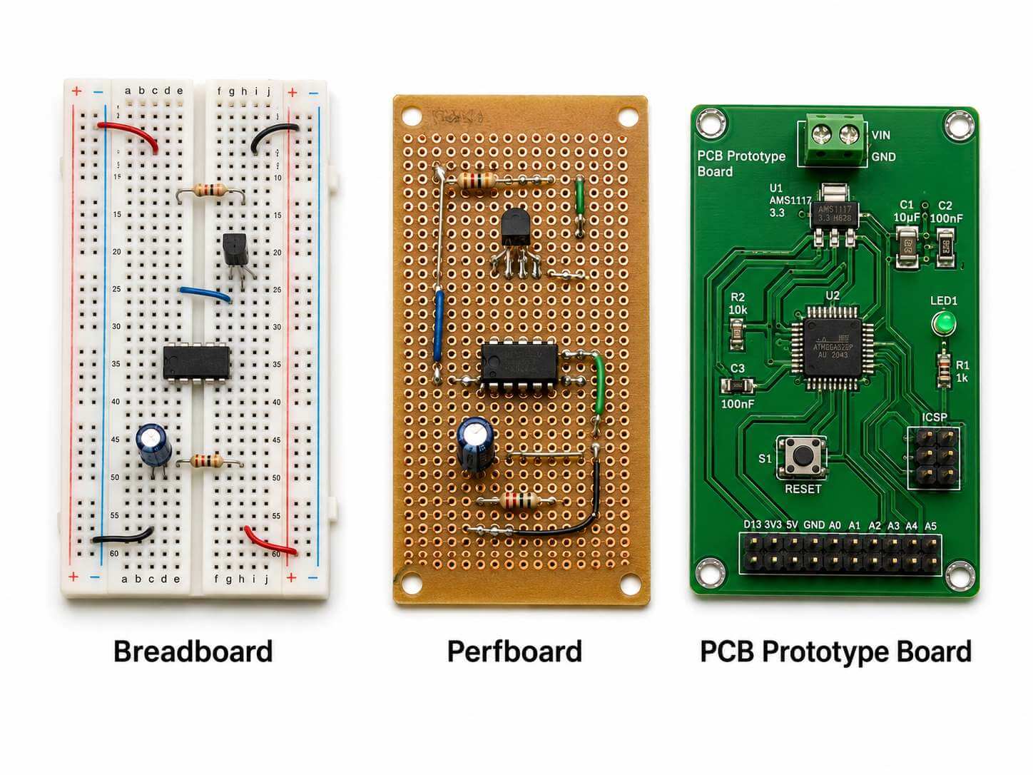
DIP vs SIP, SOIC, SMD, SMT, and THT
SMT, SIP, SOIC, THT, and DIP are often grouped together. Each term describes a different package, mounting category, or assembly process. Grouping them together can cause designers to mistake a device classification or an assembly process for a physical package definition. For example, if a designer reads SMT and treats it as a package design, they may search for a board footprint that does not exist; SMT describes what a factory does to a board, not what a component looks like.
Package names, device categories, and assembly technologies
A standard dual-in-line package (DIP), which is a common type of integrated circuit (IC) package, has through-hole leads that pass through holes in the printed circuit board (PCB). The small-outline integrated circuit (SOIC) package uses gull-wing leads on the surface pads of the PCB. The lead-geometry difference is what drives the PCB footprint and assembly route, so when you confirm the package suffix of a part number, you determine which lead form applies to your order; the device family name does not indicate which lead form applies.
Surface-mount device (SMD) and surface-mount technology (SMT) are not synonymous, as SMD refers to the actual component and SMT refers to the process of placing and soldering a component on a PCB. The same distinction applies to through-hole devices: DIP is an IC package, while through-hole technology (THT) refers to the mounting technology used to assemble the PCB.
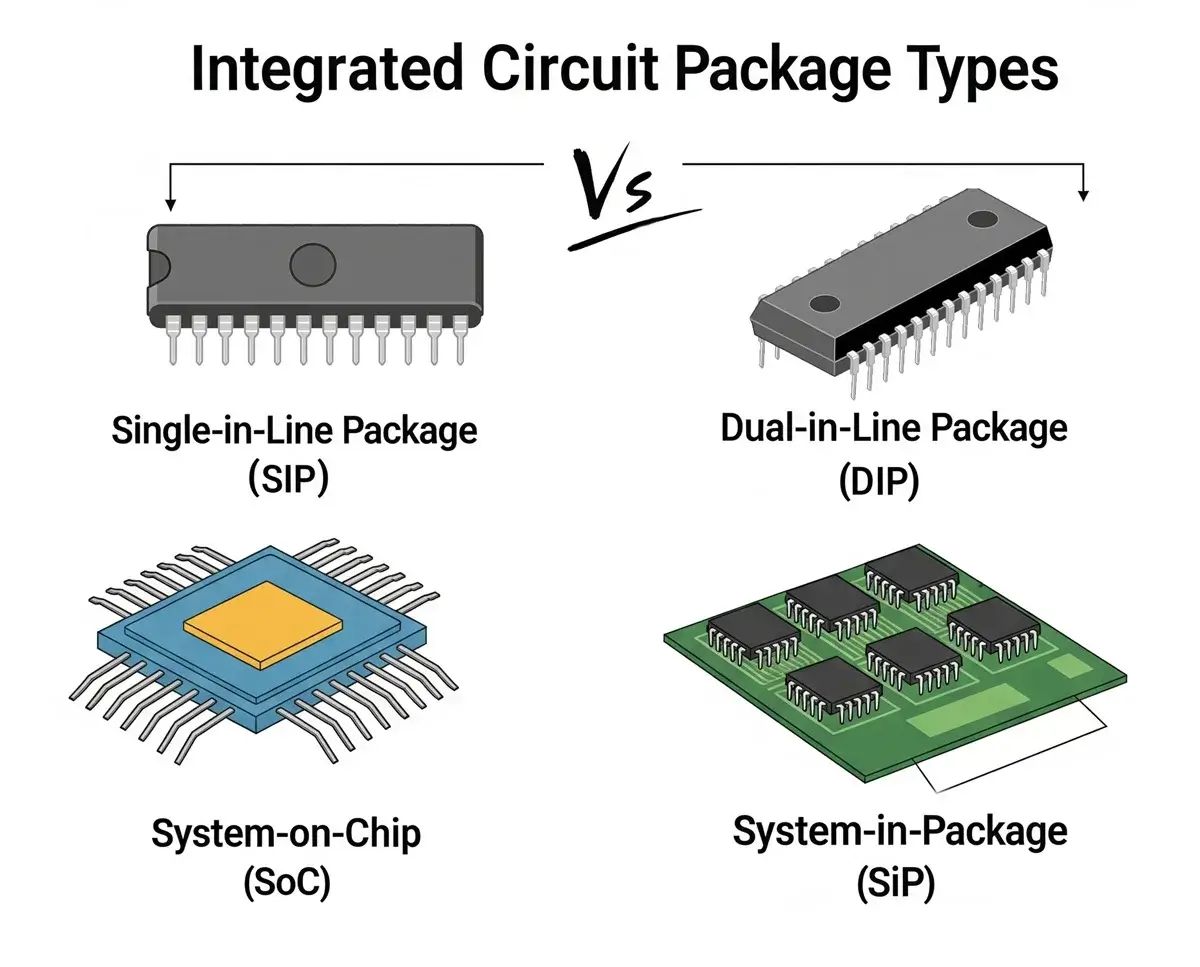
DIP vs SMT for PCB Design and Assembly
In practice, an engineer may compare a through-hole DIP option with an SOIC or another surface-mount package from the same or a similar device family.
Practical differences between a through-hole DIP option and a surface-mount option
For example, a laboratory instrument using a replaceable calibration device can take advantage of the “socket” interface on the PCB. A small form factor (SFF) communication device will typically benefit from shorter interconnection distances and more compact routing. In the case of a mixed-technology PCB, the typical use will be SMT for the majority of the components, with through-hole components only being used when mechanical, electrical, connector, servicing, or supply criteria warrant the additional use of through-hole components.
Advantages and Limitations of DIP Packages
DIP packages continue to be relevant as they are readily visible and easy to handle using hand-soldering techniques without the need for optical magnification or specialized rework equipment.
Through-hole leads also establish a direct mechanical anchoring connection to the PCB; however, the degree of anchoring for a through-hole lead will depend upon several conditions, such as the PCB material, the size of the drill hole, the quality of the solder joint, the mass of the component mounted through the holes, the vibration profile of the application, and any strain relief added in the area around the component. Therefore, DIP is not “universally” superior or more reliable without taking into consideration the previously noted conditions.
Many of today’s IC families are available solely in a surface-mount configuration; consequently, there is a risk that as technology advances and ICs are offered in fewer DIP package styles over time, the number of options for replacement devices that can be used on older circuit boards will diminish, regardless of how well the original designs continue to perform. Sourcing risk is commonly longer-lasting than the density or routing tradeoffs associated with mounting through-hole ICs.
Where Are DIP Packages Still Used?
DIP packaging is primarily found in applications where ease of handling, accessibility, ability to repair, suitability for an existing PCB footprint, or suitability for a specific available device outweighs the need for maximum component density.
Breadboard Prototyping
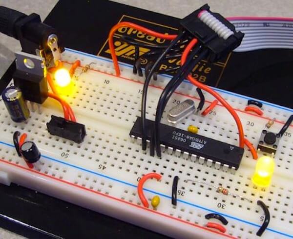
Standard-size DIP ICs using a 2.54 mm pitch continue to offer advantages when breadboarding because the ICs’ two rows fit on opposite sides of the center channel of the breadboard. Check the pitch, whether the rows of the package fit on the breadboard properly, and whether the IC’s body size leaves adequate space for power supply connections, decoupling capacitors, signal connections, and test connections. Repeated insertion into the breadboard can also lead to bent or spread pins, while larger IC package sizes can block access to adjacent connection points on the breadboard. Surface-mount-only parts usually require a breakout board to adapt the footprint of the IC to the breadboard layout.
Education and Laboratory Work
DIP package design exposes each pin, enabling easy connection to a meter or oscilloscope probe. This is an advantage for teaching students about logic, analog circuits, microcontrollers, memory, and interface ICs. The most frequent error made by students is incorrectly interpreting the pin diagram and inserting the IC with the wrong orientation or rotated 180 degrees. A DIP socket can also help prevent solder damage on the PCB from repeated soldering, but pin bending may occur during removal of the IC. If an IC extractor is used to remove the IC, lifting both ends slowly is safer than trying to remove one end quickly by using leverage.

Socketed Repair and Field Replacement
DIP sockets are used in equipment designed for use with replaceable processors, programmable memory devices, calibration components, programmable logic devices, firmware ICs, and control ICs. A replacement DIP package must match the physical dimensions of the original DIP and must have the same pin functions, voltage ratings, timing specifications, logic threshold levels, temperature ratings, and programming or configuration requirements. A DIP socket should provide sufficient retention and contact conditions for the intended location. In equipment that is subjected to vibration or contains contaminants, a poorly seated contact or an oxidized contact can give the appearance of a failed IC and may complicate troubleshooting.
Legacy Equipment
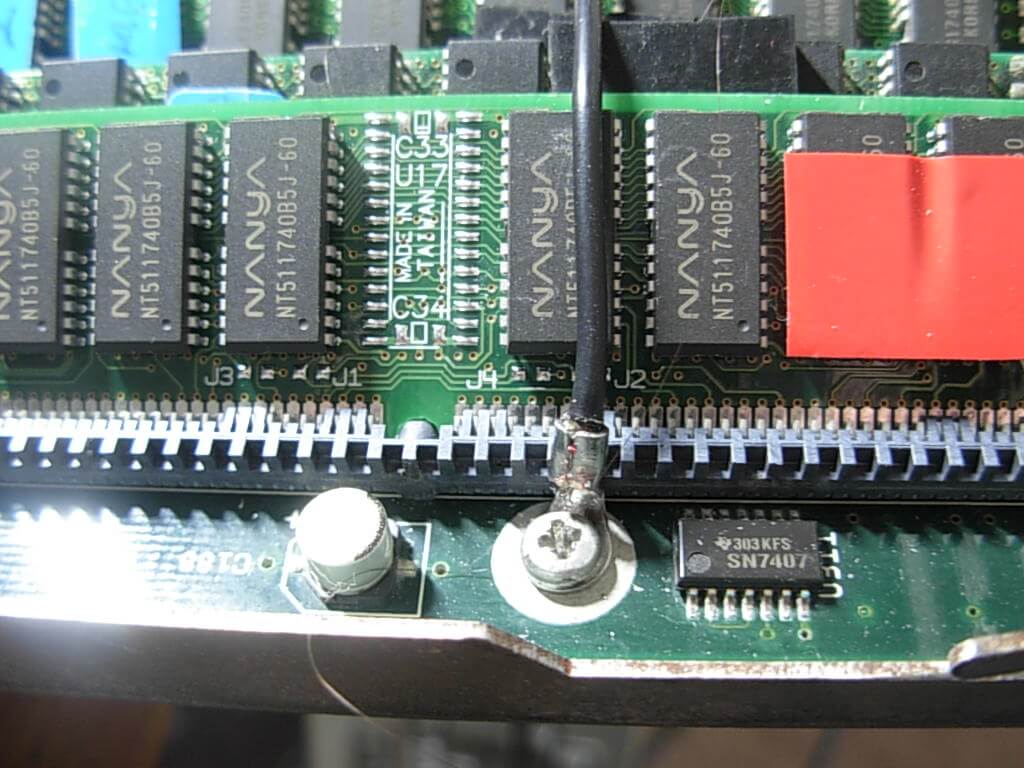
Legacy systems, such as industrial controllers, laboratory instrumentation, arcade systems, audio equipment, and older computers, may contain DIP footprints that cannot be altered without redesigning the entire PCB. In some cases, functional equivalents may now be available only in SOIC, TSSOP, PLCC, or similar packages, thereby requiring the use of an adapter board. Adapters for DIP packages must maintain the same physical orientation and electrical pin mapping, provide adequate clearance and height, and preserve signal integrity and access to adjacent devices. Simply replacing one DIP package with another DIP package of the same pin count can damage the board or components when the electrical connectivity or characteristics are different.
Industrial and Low-Volume Controls
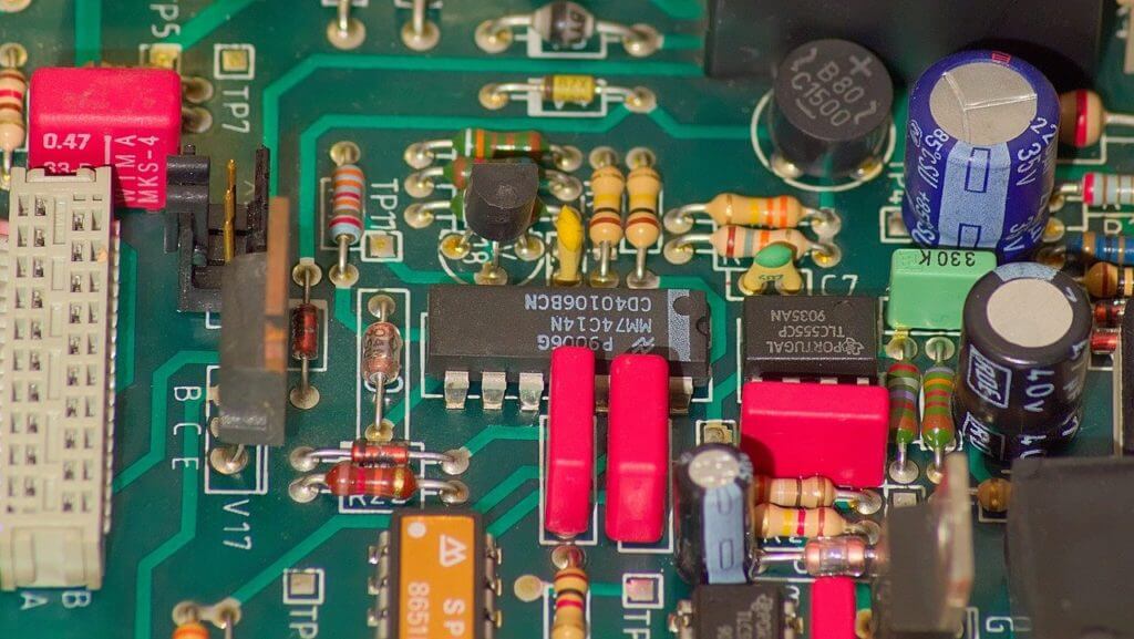
In low-volume industrial control applications, it may still be practical to use DIP-packaged logic, optocouplers, resistor networks, driver circuits, and configuration devices where ease of manual placement, ease of inspection, easy access for repair, or a known working design outweigh any advantages that may result from higher board-density goals. If a particular board design is mostly composed of surface-mount technology (SMT), it may require separate insertion and soldering phases for select through-hole-packaged DIP parts. Each of the three soldering methods (wave soldering, hand soldering, selective soldering) imposes different keep-out, thermal, masking, and inspection requirements, all of which must be considered when choosing the type of packaging and assembly route and will be reflected in the final design footprint.
What Do DIP Switch, DIP LED, and DIP Assembly Mean?
When referring to DIP in conjunction with products and manufacturing applications, DIP does not mean a generic dual-inline integrated circuit (IC) package design.
DIP Switch
A DIP switch consists of several manually operated switches packaged in one small housing. Each switch position may be used to set or configure an item’s address, options, termination, or hardware configuration. DIP switches are available in various forms, such as slide, piano, rocker, and rotary switches. Despite the name, a DIP switch is not an IC, nor does it need to be a through-hole component. Manufacturers offer DIP switches in straight-pin, right-angle, gull-wing, full-pitch, or half-pitch versions.
DIP LED Display
In the LED display industry, the term DIP refers to individual pixels associated with multiple through-hole-mounted LEDs. A full-color pixel may consist of three discrete red, green, and blue lamps, whereas an SMD (surface-mount device) display will generally comprise those colors integrated into a single compact package that is surface-mounted onto the PCB. The terminology describes both the display construction and the optical design. The definition does not describe the physical dimensions of an IC socket or PCB footprint .

DIP Assembly
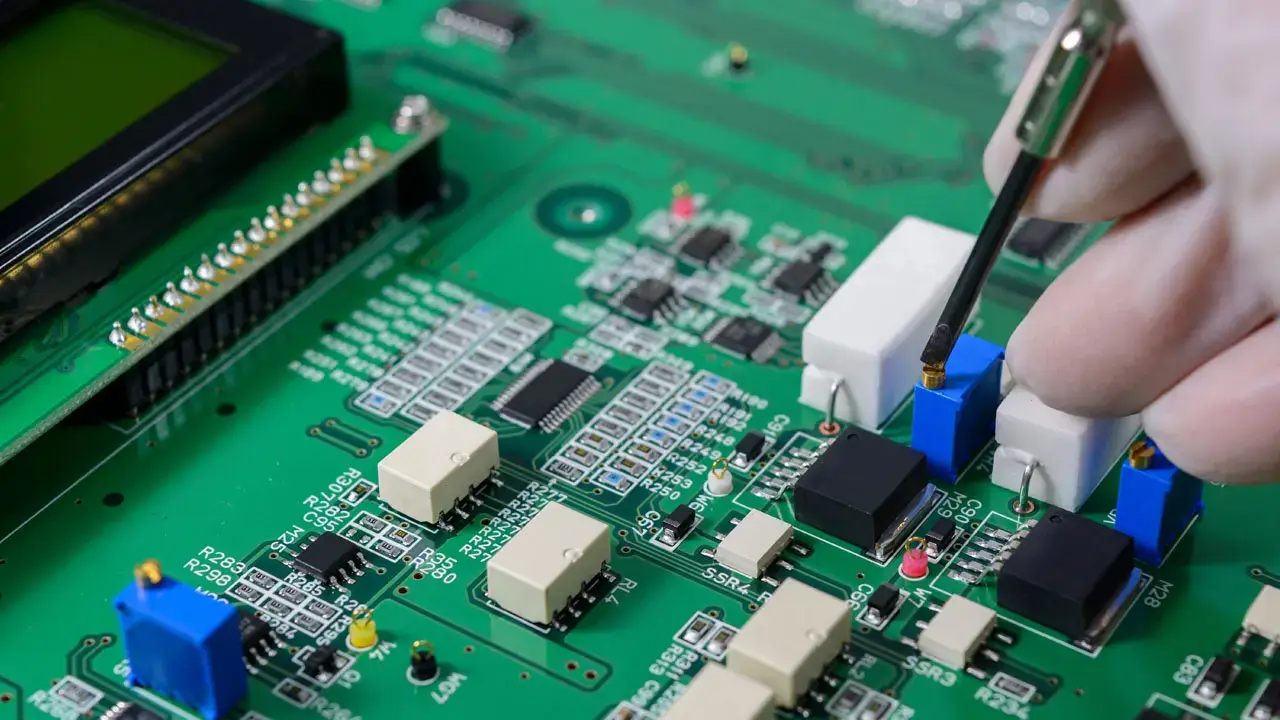
The term DIP assembly is sometimes used by PCB or circuit board manufacturers to describe through-hole insertion and soldering of components. This process may include various types of connectors, transformers, relays, switches, capacitors, or other leaded components, not just dual-inline ICs. Through-hole and surface-mount work are treated as two separate categories of assembly within IPC training materials; the use of “DIP assembly” is therefore similar to other terms that blur the lines between process areas and component packages.
Are DIP Packages Still Used?
Yes, selected devices are still available in DIP variants, although part numbers may vary. Microchip lists the 24LCS21A serial EEPROM in both 8-pin PDIP and SOIC packages. Although dual listings are available for some devices, it should not be assumed that a DIP option will always be available as a substitution or replacement. Check the most current ordering page for the specific part number.
Today, DIP-type packages are used most frequently when a particular issue must be solved by using a DIP package; examples include breadboarding, hand assembly, on-site repair, socketed replacement, legacy compatibility with a pre-existing product design, or an existing PCB that has already been qualified for production. Newer compact designs tend to be dominated by surface-mount packages, while many mixed assemblies still retain through-hole devices where the need is justified by one or more of the following criteria: mechanical, service, electrical, or supply-chain considerations.
When searching for a replacement part, use the current orderable part instead of the previous historical reference. Confirm that the new device is electrically equivalent before comparing the actual device package dimensions and target PCB geometry. An electrically suitable replacement may require an adapter or a revised PCB rather than a forced substitution.
Conclusion
Dual inline packages are defined by their two rows of pin terminals, but the term only describes the component form, not a universal PCB footprint. The best way to ensure that the choice of a DIP-type package is sound is to identify the complete manufacturer part number, including the electrical pinout, package suffix, dimensional drawing, and orientation of Pin 1. If only the DIP label, number of leads, or nominal pitch matches, many crucial compatibility questions remain unanswered.
References & Sources
- 1. Texas Instruments, CDx4HC11 Triple 3-Input AND Gates datasheet (Rev. F).
- 2. Mill-Max, IC Sockets / TO Sockets catalog and shrink-DIP socket selections.
- 3. Analog Devices, AD586 High Precision 5 V Reference Data Sheet (Rev. G).
- 4. Microchip Technology, TC4420/TC4429 6A High-Speed MOSFET Drivers, package drawings.
- 5. ICC, DIP and SIP Sockets.
- 6. NXP Semiconductors, AN11267 EMC and system-level ESD design guidelines for LCD drivers.
- 7. E-Switch, What Are DIP Switches and What Are Their Uses?
- 8. Same Sky, DIP Switches 101.
- 9. Rotapanel, Understanding Different Types of LED Displays: SMD vs. DIP.
- 10. Microchip Technology, 24LCS21A 1K 2.5 V Dual Mode I2C Serial EEPROM datasheet.
- 11. IPC, Electronics Assembly for Operators – Instructor Guide.
- 12. Different IC Packages Explained | DIP, SOIC, QFP, QFN and BGA Packages Explained — ALL ABOUT ELECTRONICS.