Upload BOM & Gerber

Voltage Reference, Current Return, PCB Grounding, and Safe Measurement
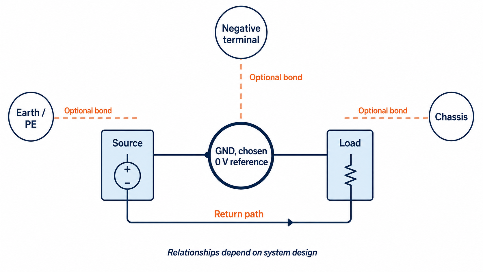
An abbreviation for ground in the electronics field, GND is commonly used as a voltage reference, a current-return path, and a potential connection to either Earth or a chassis. The power architecture, isolation barriers, connectors, and enclosure design of each piece of electronic equipment determine which functions GND performs.
Read any GND label with three questions: What voltage reference does it establish? Which current returns through it? What is it intentionally bonded to?
Contents
show
What Does GND Mean in Electronics?
GND is a common reference point for all voltages within a circuit. If a signal indicates a voltage of 3.3 V, it can be understood as 3.3 V above GND. By establishing a reference voltage, GND allows the voltages present in the circuit to be identified and measured, even though the actual voltage at GND may vary from its reference value under changing load conditions.
GND may also carry return current from a power rail or signal conductor through the GND net or node. The reference and return aspects of GND work together within electronic circuits; however, even though GND is a voltage reference, it does not necessarily have a physical connection to Earth. PE serves a safety function and is used to conduct fault current, never normal operating return current.
In most schematic drawings, repeated GND symbols represent the same logical net defined by the connectivity scope within a design tool. As a result, designers do not have to indicate every wire that connects to GND, the entire physical return path for current back to the power source, the impedance of that path, or every connection from GND to shielding, chassis, or Earth. Net names, hierarchical scope, net ties, connector pinouts, and system documentation define what a net name means.
Why Is GND Called 0 V?
GND is identified as 0 V because the designer or system architect has chosen it as the voltage reference point for the circuit design. Voltage is defined as the difference between two points and requires a specified or implied reference point.
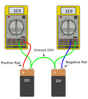
If you take the example of an isolated 5 V supply with the negative output connected to GND, that places the positive output at +5 V relative to GND. If a different configuration connects the positive output to GND, the negative output is indicated as -5 V relative to GND. The isolated 5 V source still has the same terminal-to-terminal voltage of 5 V; only the chosen voltage reference and the resulting voltage labels have changed. Therefore, in most cases, GND will be the negative terminal of a single-supply circuit, but this does not mean it is always negative.
There are situations where a circuit can float relative to Earth while its internal voltages remain defined. Examples include battery-powered devices, isolated DC/DC converters, and some bench power supplies. Connecting a USB cable, programmer, oscilloscope, grounded load, or chassis bond may create a new Earth relationship that was not previously established.
A virtual ground is typically created as a reference point near the centre of the voltage range between the supply rails of a single-supply circuit. The single-supply circuit can process signals above and below this reference point. The source and sink capability, output impedance, stability, and response time of the GND reference also determine how much return current the ground point can support before its voltage deviates from the reference voltage.
How Does Current Return Through GND?
The most basic rule for current is that it flows in a complete circuit back to where it originated, even though it may pass through a GND symbol on a schematic. In the example of a battery-and-resistor configuration, conventional current leaves the positive terminal, flows through the load, and returns to the negative terminal. When that returning conductor is labeled GND, GND refers to the reference point and connectivity of that conductor, and the current continues to flow through that point back to the battery.
In practice, there may be several ground currents flowing simultaneously through different areas of the GND network. For example, logic outputs, voltage regulators, analog sensors, motor-drive circuits, cable-shield currents, protection devices, and decoupling capacitors are all sources of GND return currents. Some return currents may use the same physical copper trace to return to the GND reference point, while others remain local to where they are injected, and others meet at a specific point in the GND network. The full electrical circuit and total impedance of each return-current path determine how these return currents flow back to the GND reference point.
At DC and low frequencies, resistance dominates the voltage drops associated with each return-current path. As the edge rate or frequency of a signal increases, inductive reactance, loop area, plane continuity, and proximity to reference structures have an increasing influence on the return currents. High-frequency return current generally remains close to the associated signal path when a continuous plane is available as a ground reference. Gaps in the conductive plane, such as slots or split ground planes, poorly placed vias, and distant decoupling capacitors can force the return current to take a longer path, leading to additional noise and radiation.
Where the return current physically travels is dictated by the copper and via geometry. The physical placement of GND symbols in a schematic provides no information about the actual current flow within the GND network; the GND symbol at the bottom of the page is merely a drafting convention, and the voltage at two GND symbols may differ under load even if the two points belong to the same logical net.
How Is GND Different from Negative, Neutral, Earth, PE, and Chassis?
In a product, several different reference systems may exist; they may be bonded at one point, connected through an impedance, capacitively coupled, or completely isolated. In any case, a schematic label alone cannot indicate the interconnection between those different reference systems.
Mixing up neutral (current return) and PE may cause an error when measuring an AC-powered circuit: a technician may clip a lead to neutral and expect the same protection as when using PE. Technicians need to be aware that neutral carries normal load current and, during a fault condition or with a broken conductor, may be well above 0 V relative to Earth. A PCB label such as GND does not specify which of these two reference systems, if either, it eventually reaches.
Another parallel error occurs when assembling chassis and shields. A shield connected to chassis at a single connector provides an intended path for high-frequency common-mode current. If the same shield is connected again at a second connector or bonded to circuit GND at a point that was not planned in the original single-point design, it can create a second path that may lead to a hum or emissions problem. The resulting problem can be traced to the additional connection, not to a design flaw.
What Do Ground Symbols and Labels Mean?
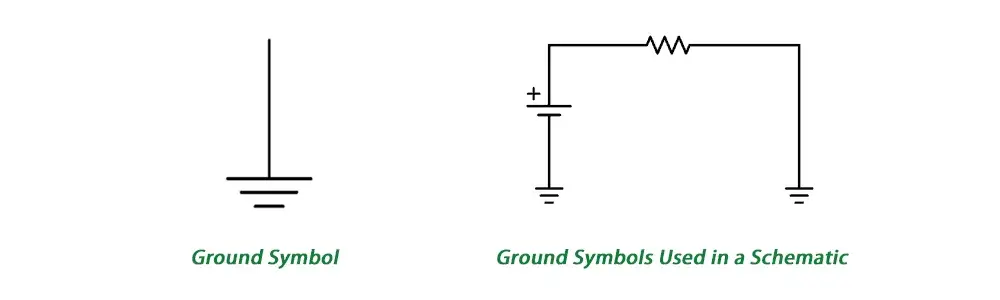
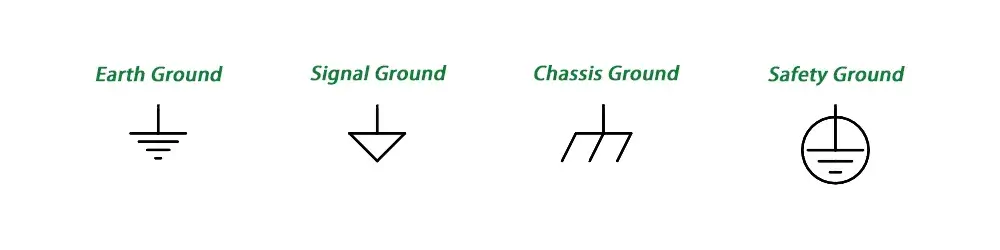
Ground symbols indicate the type of reference system intended by the designer. The interpretation of a given symbol depends on the schematic legend, CAD library, net name, and product architecture. In addition, similar-looking symbols may have completely different meanings at different companies. Understanding the meaning of a ground symbol requires reading the drawing as a whole: the legend, netlist, and hierarchy.
Common Ground Symbols
A circuit-ground symbol is used to designate the local electrical reference and return network of the circuit. To confirm whether the local electrical reference has an actual Earth connection, the designer must check the netlist, not simply rely on the symbol. An Earth symbol indicates an intentional connection to an Earth-referenced system. The drawing should clearly specify whether the connection to Earth is for functional or protective purposes. The PE symbol represents the protective conductor and is used for touch-voltage safety and to conduct fault current. A chassis symbol indicates the metal frame or enclosure of the device, which is bonded to circuit GND only where a specific note or component makes that clear. A signal-ground symbol indicates a signal-reference domain. How that domain joins power ground or chassis is a separate design decision that the symbol alone does not convey.
Repeated ground symbols must follow the CAD connectivity rules. A global ground symbol may connect multiple sheets within a project, whereas a local ground symbol or hierarchical net may remain within a single design block. Net ties and zero-ohm links can intentionally connect nets that retain different names. Reviewing only the printed symbol without checking the netlist can therefore lead to the wrong conclusion.
AGND, DGND, PGND, SGND, and Related Labels
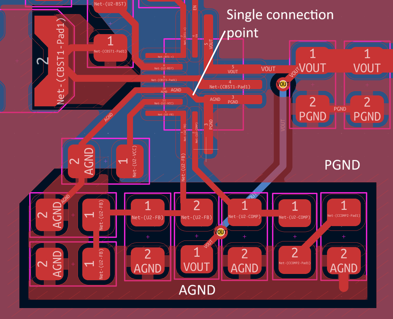
Typically, the prefix identifies a current domain, functional domain, or component pin purpose. The prefix is a clue for tracing the reference, return path, and bond; it is not a universal instruction to split the ground plane.
The AGND and DGND pins can be connected to a shared low-impedance plane or through a controlled low-impedance connection according to the manufacturer’s specifications. However, a split plane is not automatically quieter. When a signal crosses a split plane, the return current may have to flow around the gap, increasing the loop area and coupling. Component placement and return-current control will have a greater effect than the printed name of the pin.
PGND also requires special consideration because it commonly carries pulsed current from switching converters, gate drivers, LEDs, solenoids, and motors. Thus, the point at which PGND connects to a quieter reference may be less important than keeping its high-current loop compact and preventing PGND from sharing impedance with sensing or control returns.
How Does GND Work on a PCB?
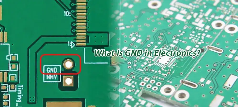
The PCB translates the logical GND net into copper pours, planes, traces, vias, pads, connector pins, mounting points, and controlled bonds to chassis or shield. The quality of the GND network is based on its geometry and current distribution, not on the number of GND symbols shown in the schematic.
Keep the Reference Path Continuous
By providing a continuous GND plane, the PCB allows signals and decoupling currents to have a nearby low-impedance return path. High-speed traces should not cross plane splits, slots, voids, or reference changes unless a designed return path is provided. When a signal route changes layers, a nearby ground via provides a path for return current between reference planes. If such a path is not available, return current may reroute through distant stitching vias or connectors. This can increase both loop area and emissions.
Control High-di/dt Loops
Current changes produced by switching regulators, motor drivers, gate drivers, and pulsed loads can occur very quickly. Their input-capacitor loops, switching-node loops, rectifier loops, and output-capacitor loops should therefore be kept as compact as possible. Adding wider copper alone will not reduce emissions if the actual loop is large or the return path shares a narrow connection with analog ground. When designing the circuit layout, place the components that exchange pulsed current close together and connect their returns locally before connecting them to quieter areas as required by the overall circuit design.
Place Decoupling Where the Current Is Drawn
Decoupling capacitors provide local transient current between the power pin of the device and its reference pin or plane. Long traces, distant vias, and narrow necks add inductance and reduce effectiveness. The path used to supply current to the device and return it to the capacitor forms the complete decoupling loop. This loop should be as direct and short as possible.
Partition Functions Without Blindly Cutting the Plane
Digital, analog, RF, and power circuits should be positioned so that their dominant return currents remain within their intended regions. This functional separation between circuit sections can often be achieved over one continuous ground plane. Any cutting of the ground plane should be implemented deliberately as part of the overall electrical design, based on the device data sheet and the circuit’s signal-routing plan.
Use Controlled Connections Where Separate Nets Are Required
Depending on the application, different nets can be connected using net ties, zero-ohm jumpers, ferrite beads, capacitors, RC networks, or chassis bonds. A net tie creates a defined connection point while preserving separate net names. A zero-ohm jumper provides a configurable DC connection. A ferrite bead provides frequency-dependent impedance; however, it can also develop a voltage under current and may resonate with connected capacitance. A capacitor can provide a high-frequency path without providing a DC connection. Choose the interconnection method according to the current, voltage, EMC, safety, and service requirements.
Why Is GND Not Exactly 0 V Everywhere?
The schematic representation of all components connected to the GND net will show that they are connected to the same point; however, physical conductors have resistance and inductance. When current flows through that impedance, localized voltage differences appear. The real-world reference point for GND is represented as nominally 0 V, but it is not truly at 0 V at all locations and at all times.
Ground Offset
Ground offset refers to a voltage difference created by current flowing through resistance. The formula for calculating ground offset is voltage offset = current x resistance. The copper path through a connector contact, cable, trace, via field, mounting screw, or narrow copper neck may appear to be a short circuit during an unpowered resistance test; however, it can develop a measurable voltage under load. This is especially important for devices with millivolt-level outputs whose return paths share copper with ampere-level loads.
Ground Bounce
Ground bounce refers to a rapid change in the local ground reference caused primarily by changing current through parasitic inductance. Ground bounce is proportional to L x (di/dt), where L is inductance and di/dt is the current slew rate. Fast logic outputs, gate drivers, memory interfaces, and switching power stages can shift the local ground reference enough to alter thresholds, disturb ADC results, or cause false switching, even while the average DC ground voltage appears normal.
Ground Loops
A ground loop occurs when two points are interconnected by more than one conductive path and a voltage difference causes unintended current to flow around the resulting loop. Common examples include a USB cable together with a separate grounded power supply, an audio cable between two Earth-referenced devices, or multiple chassis bonds connected through a rack.
An unwanted path can produce audible hum, measurement errors, common-mode current, or EMI. The appropriate remedy depends on whether the unwanted path is DC, low frequency, or high frequency. Removing every bond can create a safety or EMC problem.
A shared GND name provides logical connectivity, yet conductor resistance and inductance may cause two physical points on the same GND net to have different instantaneous voltages. The relevant question is whether the voltage difference between those two points remains within acceptable limits for signal accuracy, noise margin, EMC, and safety under the actual current and frequency conditions.
How Do You Identify and Measure GND Safely?
Properly identifying GND means more than locating a point where a multimeter or continuity tester beeps. Schematic connectivity, power-state measurements, dynamic measurements, and instrument grounding answer different questions.
Unpowered Continuity Test
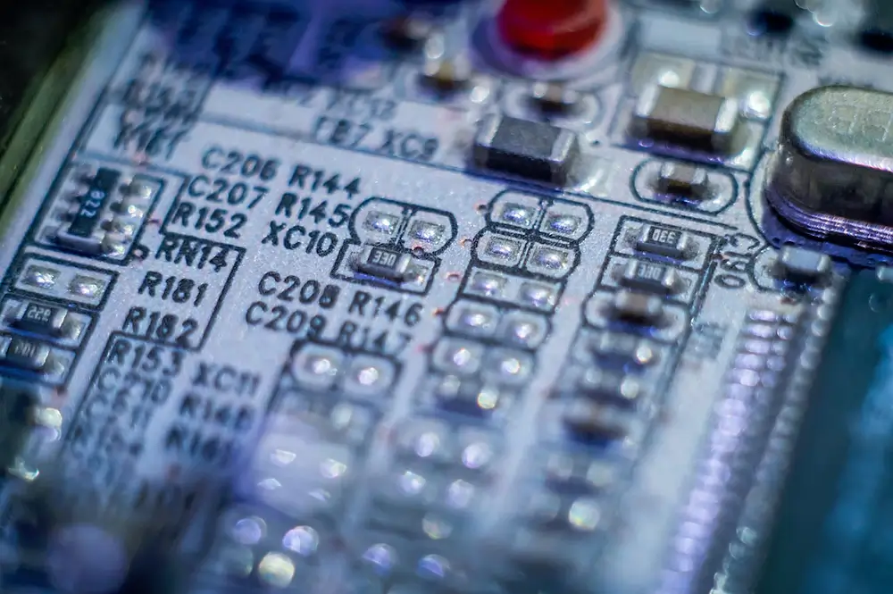
With power removed and stored energy discharged, a continuity test can show whether a conductive DC path exists between two locations. The continuity test is useful for verifying that a connector pin, test pad, mounting point, or component pin is part of the expected ground network. Resistance mode can provide additional information when the path contains a resistor, ferrite bead, inductor, protection device, or semiconductor junction.
A continuity test does not verify that the path provides sufficiently low impedance under operating current. It may also fail to identify contact resistance, a narrow copper neck, a weak solder joint, current-dependent heating, or high-frequency inductance. A path that shows continuity at a few milliamperes may still produce significant voltage drop or noise when the product is powered.
Powered Voltage-Drop Test
A powered voltage-drop test measures the voltage difference between two ground points while the circuit operates under its normal or worst-case load. It can reveal connector resistance, long cables, insufficient copper, shared high-current return paths, loose fasteners, and load-dependent ground offset. Measuring across the suspected path is typically more useful than measuring both ends separately against a distant reference.
A handheld meter often provides an average or relatively slow response. It may miss nanosecond- or microsecond-scale ground bounce, switching spikes, and ringing. A low DC reading does not prove that the reference remains stable during digital edges or power-switching events.
Oscilloscope Measurement
An oscilloscope can show dynamic activity that a multimeter cannot detect. This includes ground bounce, switching spikes, common-mode transients, ringing, and reference movement associated with clocks or load steps. Probe connection geometry can affect the measured waveform. A long ground lead adds inductance and can distort or exaggerate the measurement. For fast, low-amplitude measurements, use a short spring ground or a suitable differential probe.
Displaying a waveform does not guarantee that the connection is safe. On a conventional Earth-referenced oscilloscope, the probe ground clip is typically connected through the instrument to PE. Connecting the clip to a floating node, an offline power-supply primary reference, or another point that must not be Earth-referenced can create an unintended short circuit, damage the equipment, or expose the user to hazardous energy.
Before probing, verify the relationship between the test point and Earth, the oscilloscope input architecture, the probe voltage and common-mode ratings, and the measurement method permitted by the equipment documentation. A floating or high-side measurement may require a suitably rated differential probe, an isolated-input instrument, or another approved isolation strategy. Removing PE from a standard oscilloscope is not a safe substitute for a proper measurement system.
Real GND Examples in Electronic Systems
Battery-Powered Sensor
A battery-powered sensor may have a completely floating internal GND. Its ADC, microcontroller, and radio can still use it as a stable 0 V reference point. This relationship changes when the sensor is connected to an external device, such as a USB programmer, grounded oscilloscope, charger, or shielded cable. Once an external connection is made, the sensor GND may be bonded to Earth or to another device’s ground, creating a new common-mode path.

When testing the product during production, the same risk occurs at the test fixture or programming station. For example, if a bed-of-nails probe or pogo pin is wired to a grounded ICT fixture chassis, it might inadvertently bond to the floating GND once the board is loaded onto the fixture, unless the test specification expressly states the grounding configuration for the test points and fixture. Debugging a prototype should include comparing the standalone and connected configurations rather than assuming that the battery maintains isolation during every measurement.
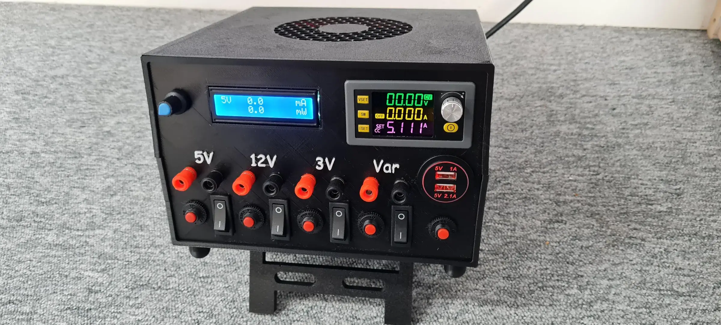
Floating Bench Supply
Most isolated bench-supply outputs remain disconnected from chassis Earth until the user makes that connection. Grounding the negative output produces the familiar positive supply. On the other hand, grounding the positive output produces a negative voltage rail relative to Earth, provided the instrument ratings allow it. Connecting two output channels in series establishes another reference relationship.
Assuming that the black terminal, green chassis terminal, and oscilloscope ground clip are all at the same potential is a common trap. This trap can also affect FAI verification of isolated boards when the polarity of a supply rail is checked against a floating output rather than Earth. Adding an explicit step to verify the supply-rail polarity against the intended reference before running a full production batch can prevent boards from being tested against the wrong reference.
USB-Powered Device
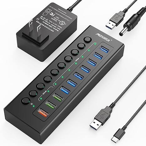
A USB-powered board shares its circuit GND with the return conductor of the cable and often with the chassis of the host computer. Connecting the board to an audio system, benchtop power supply, debugger, or oscilloscope can create another path between the same grounds. Low-frequency potential differences can create hum, while high-frequency common-mode current can flow through the cable shield and connector shells.
The board design should distinguish the signal return, shield termination, chassis bond, and ESD path. This is what a reviewer should check during a layout review of the connector footprint: whether the shield tab of the USB connector lands on its own keep-out pad tied to chassis, separate from the signal-return trace. This allows the reviewer to confirm in the Gerber data that the two paths are separated before the board is built, rather than after a hum complaint occurs.
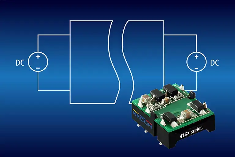
Isolated DC/DC or Communication Interface
An isolation barrier produces two different reference domains. GND_A and GND_B cannot be considered interchangeable, even though they are labeled GND on different sides of a digital isolator, isolated transceiver, or DC/DC converter. Although there may be no DC continuity between the two grounds, transformer or capacitor parasitics can still permit high-frequency common-mode current to pass across the isolation barrier.
The path of that common-mode current depends on creepage, clearance, Y-capacitor selection, shield strategy, and connector placement. Connecting GND_A and GND_B together, whether accidentally through a test instrument or through mounting screws, can defeat the intended isolation. A layout review checks creepage and clearance across the isolation barrier against the voltage-based spacing tables in IPC-2221 and the working voltage specified for the project. Without that working voltage in the design input, no reviewer can verify that the isolation gap on the board supports the isolation assumed by the schematic.
Offline Switch-Mode Power Supply
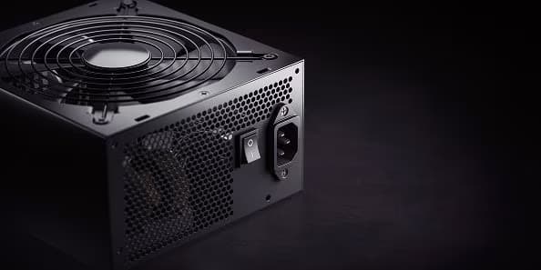
The primary reference for an offline switch-mode power supply is typically referred to as primary ground or hot ground. This reference can be at a hazardous potential relative to Earth. It is not PE and should never be assumed to be safe to touch. The secondary GND may float, connect through a controlled network to chassis, or connect directly to Earth, depending on the equipment class and EMC architecture. Connecting an Earth-referenced probe ground to the primary reference can create a destructive fault.
A hipot or insulation-resistance test across the primary-to-secondary barrier can confirm the intended isolation. The test applies the specified test voltage between the primary and secondary circuits and checks whether the leakage current or insulation resistance remains within the applicable acceptance limits.
Automotive or Motor-Control Module
In a vehicle or motor-control system, chassis or battery negative may carry substantial current from starters, fans, pumps, injectors, solenoids, or traction loads. Cable resistance, connector resistance, weld-point resistance, and copper-path resistance can create a ground offset between a sensor and the controller, causing the sensor reading to appear inaccurate when measured against a distant power ground.
Several methods can minimize this condition, including separate sensing returns, Kelvin connections, local filtering, and controlled joining points between sensing and power returns.
A layout or DFM review can identify an issue related to ground-reference locations in the netlist. For example, if a Kelvin sense return from the load shares the same net name and copper path as the high-current power return it is intended to measure independently, the resulting shared impedance can create inaccurate or noisy readings once the PCB is populated and loaded.
Conclusion
Before assuming what a GND label means, three points must be checked: which voltages use it as their reference, which currents complete their paths through it, and which other reference systems it is bonded to.
On a PCB, this check includes plane continuity, loop geometry, component guidance, connectors, shielding, and enclosure strategy. On the bench, continuity testing, powered voltage-drop measurements, and oscilloscope measurements answer different questions and carry different safety requirements. Relying only on a continuity beep can allow a floating reference, hazardous primary reference, or shared return path to remain undetected until the product fails in the field or on the test floor.
References & Sources
- 1. Keysight Technologies. “What Is Ground Reference?”
- 2. Keysight Technologies. “Your Load Could Cause Unexpected Power Supply Behavior.”
- 3. Texas Instruments. “Grounding in Mixed-Signal Systems Demystified, Part 1.”
- 4. Texas Instruments. “Grounding in Mixed-Signal Systems Demystified, Part 2.”
- 5. Analog Devices. MT-031, “Grounding Data Converters and Solving the Mystery of AGND and DGND.”
- 6. Texas Instruments. “Best Practices for Board Layout of Motor Drivers.”
- 7. Texas Instruments. TLE2425 Rail Splitter data sheet.
- 8. Tektronix. “ABCs of Probes Primer.”
- 9. Occupational Safety and Health Administration. “1910.399 Definitions.”