Upload BOM & Gerber


Manufacturing printed circuit board assemblies (PCBAs) is the controlled conversion of authorized production packages, identified bare boards, and identified materials into verified PCB assemblies with traceable records. These processes are completed using machines, but they are successful only if we know that the configuration of each unit being produced is authorized, which manufacturing route applies, what each verification process proves, and who can close an exception in the manufacturing process.
Production is initiated when identified bare boards, released materials, and approved production data are in place; however, design for assembly (DFA) evaluation, stencil creation, programming, and fixture development may occur before this point. The elements of the printed circuit board assembly manufacturing process, including basic terminology, differences between printed circuit boards and printed circuit board assemblies (PCBs versus PCBAs), and common sequential process flows, have already been discussed in detail in the What Is PCB Assembly? article; however, this article will focus on configuration control, manufacturing evidence, exceptions, traceability, and final release.
When manufacturing a large volume of units over time, maintaining a cohesive relationship between the three files—the bill of materials (BOM), placement file, and assembly drawing—is ultimately what printed circuit board assembly manufacturing practices and processes are about. For example, if the BOM indicates the correct part number for design revision C, but the placement file describes assembly revision B, then a stable manufacturing line will continue to manufacture the incorrect configuration repeatedly over time. Therefore, we must ensure that the first manufacturing gate closes the release package before materials reach the manufacturing line.
- Production requires an authorized configuration, not a collection of files.
- The assembly route will vary based on the board side, package geometry, thermal limitations, physical access, and verification criteria.
- Machine or inspection records carry weight only when they identify the job, revision, operation, and acceptance decision they support.
- Inspection, structural testing, and functional testing address different questions.
- The depth of traceability should correspond to the product risk as agreed upon between the customer and supplier.
Contents
show
What Makes a PCBA Job Ready for Release?
The release gate will have the following key components: product, revision, population variant, permitted deviations, process instructions, and test definitions, all of which should be listed in one easily readable format. There are three main areas that must be reviewed as part of the job release review process:
Product configuration: The bare-board identification and revision must match the assembly order. The bill of materials (BOM), approved alternatives, intentional no-fits, placement data, and assembly drawings must clearly define the same product variant, including part position, rotation, orientation, population status, polarity, and board side.
Production requirements: Wherever special handling, hardware installation, cleaning, coating, programming, and labeling instructions affect the manufacturing route or final acceptance, those requirements must be clearly identified.
Deviations and test configuration: Any approved deviation linked to the job must include the approval authority for that deviation. Also included will be the test firmware, test fixture version, pass/fail limits, and test result format, all of which must match the same released product revision.
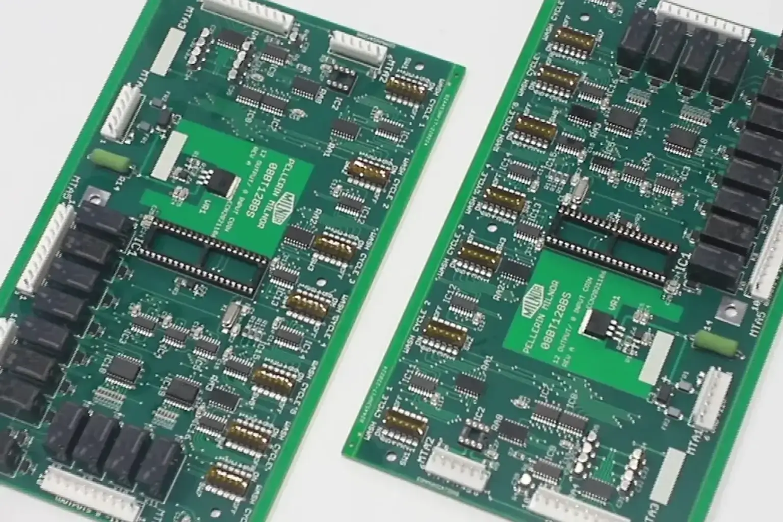
The methodology for generating output files in electronic design automation (EDA) software might lead to different outputs being provided to the manufacturer. For example, KiCad 10 documentation states that placement files contain the position and orientation of components, but EDA export settings and footprint attributes might exclude DNP, BOM-excluded, position-excluded, or selected through-hole footprints. Similarly, Altium’s output-generation documentation shows that BOMs, assembly drawings, pick-and-place files, test-point files, and other outputs can change with the selected assembly variant. Therefore, the single practical rule regarding PCB manufacturing outputs is to always generate and release related outputs from the same approved design state.
Schematic diagrams are still useful for defining the electrical configuration of a PCB and developing tests, but schematic diagrams are not sufficient to create a complete assembly package. Production should stop when any document contradicts another document. Guessing at a component rotation, substitute, or no-fit turns an unresolved design question into a manufacturing defect.
What Are the Main Steps in PCB Assembly Manufacturing?
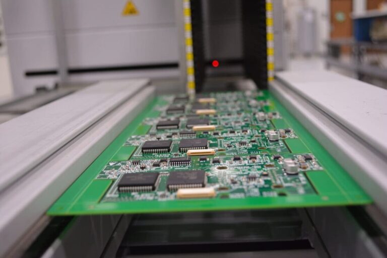
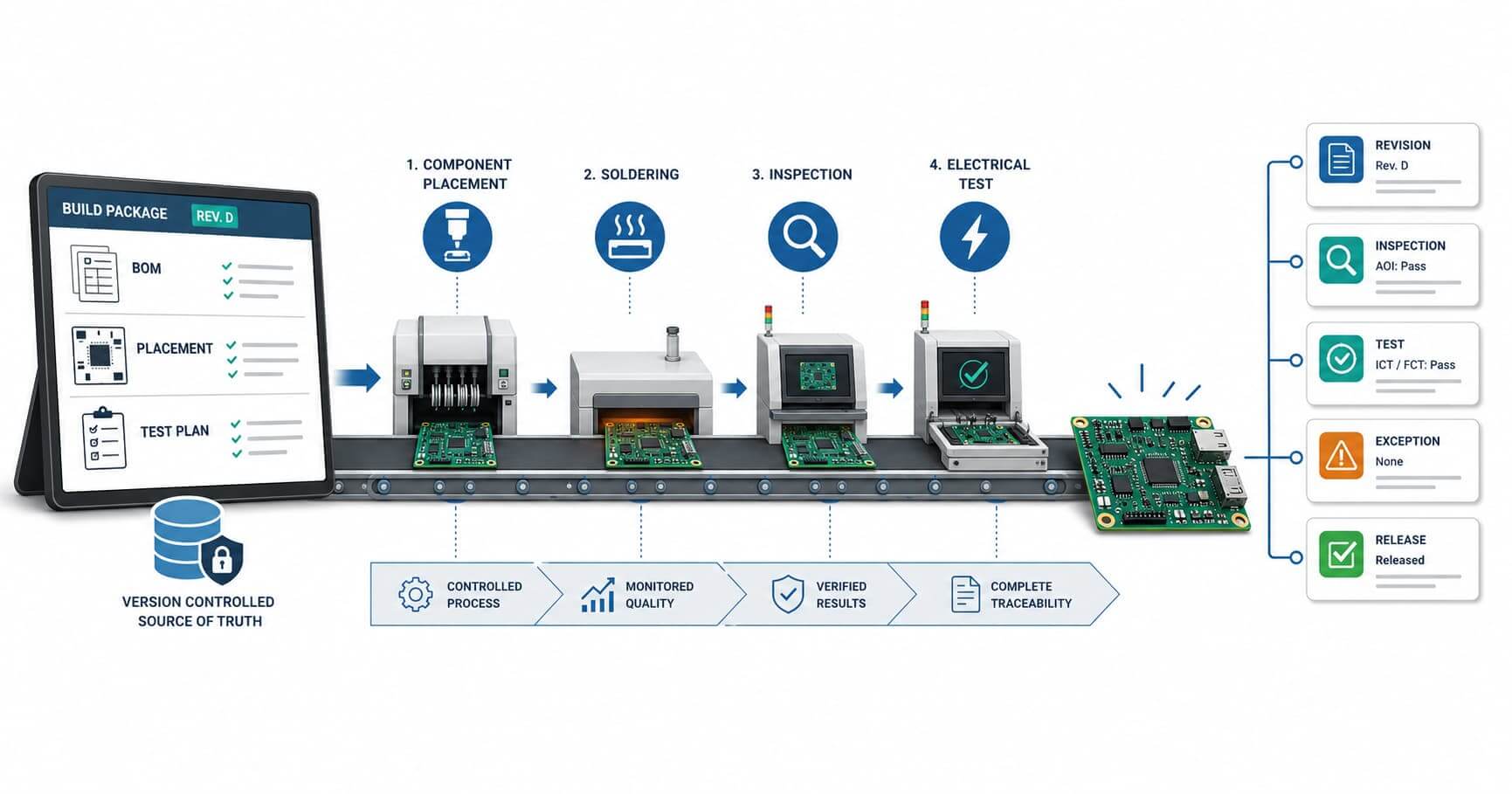
A typical PCB assembly manufacturing flow begins only after the production configuration, materials, tooling, and machine data are ready for use. For an SMT assembly, the baseline sequence usually moves from solder paste printing and inspection through component placement, reflow, and post-reflow inspection. Through-hole components, cleaning, programming, coating, hardware installation, and electrical testing are then added where the released product and process route require them.
This sequence is a reference flow rather than a fixed recipe. A double-sided assembly may require two controlled reflow passes, concealed joints may require X-ray inspection, and mixed SMT and through-hole assemblies may add wave, selective, or manual soldering. Components with cleaning, thermal, mechanical, or access restrictions can also change the order of individual operations. The manufacturing route therefore has to be defined for the actual board rather than inferred from the process names alone.
How Do Board Design and Component Technology Change the Assembly Route?
Printed circuit boards assembled using SMT, through-hole, or mixed-technology methods are referred to by their respective technologies, but using those terms alone is not sufficient to define the complete assembly route. The complete assembly route will therefore vary according to the following factors: board side, component package geometry, heat exposure, physical accessibility, feature visibility, and the need to verify features before they become hidden. The assembly process not only includes the methods by which the PCBs are assembled, but also determines where heat, accessibility, visibility, or verification requirements change the assembly route.
The assembly route must also take into account items such as panel support, component packaging, feeder and nozzle access, stencil design, compatibility with the cleaning process, programming, coating, and access to test fixtures. For example, a heavy component installed on the bottom side of a PCB assembly can dictate the order of components during the second reflow pass; non-washable connectors could require installation after cleaning the board; and closely spaced through-hole pins can prevent access to the selective-solder nozzle.
There are cases where the various constraints above do not align, and the solution is to create a processing sequence for the different items rather than apply more stringent inspection practices. For example, a double-sided PCB assembly with a heavy component installed on the bottom side would require reflow-sequence priority, while a non-washable connector must be installed after the initial cleaning phase. Therefore, in many cases, attempting to process the two components in the same sequence will involve reworking the PCB assembly rather than causing a defect outright. The same applies when selective-solder nozzle clearance is not assessed until after the design review has been completed and the PCB assembly has entered production setup. The design review process needs to take into account access for the selective-solder nozzle before the assembly is set up for production, not as an additional step after the through-hole process has already begun.
Control Starts Before the First Solder Joint
The most important first control points are released documents, material identity, handling status, stencil and tooling revision, machine programs, panel support, and verification of the first-off product. The Design for Assembly (DFA) review should address component-to-footprint mismatches, polarity or pin-1 conflicts, feeder and nozzle accessibility, fiducial and support requirements, through-hole soldering accessibility, and test-point or coating keep-out zones before production setup. The above items serve as the first line of defence against defects propagating throughout a lot or being hidden by subsequent processes.
Material readiness requires, at a minimum, linking each issued component and bare board to the job number, approved manufacturer part number, selected population variant, and appropriate handling status. When material requires drying or preparation for use, or has other material-specific restrictions, these items must be checked. Any discrepancies should warrant an exception rather than an informal substitution at the manufacturing site.
There must be a disciplined approach to tool and program configuration, meaning both must be readily linked back to the released configuration through the stencil, solder paste requirements, placement program, feeder setup, reflow recipe, inspection program, test program, and fixture. Therefore, a correct bill of materials (BOM) cannot protect an assembly if the active placement program belongs to a different revision.
While first-off verification processes are valuable for identifying configuration-related risks before production is repeated, they should include paste deposits, part identity, polarity, orientation, placement, hardware used, and a representative sample of solder and test features. First-off verification cannot substitute for later inspections; however, its objective is to ensure that the route, setup items, and released configuration have been successfully aligned during the assembly process.
Which Evidence Belongs at Each Manufacturing Gate?
The strength of any evidence file depends on the link between the evidence and its current job, revision, operation, and acceptance decision. A machine log without a clear job identity has weak diagnostic value, and a pass result without parameters or the original program revision cannot determine the conditions that dictated the acceptance decision.
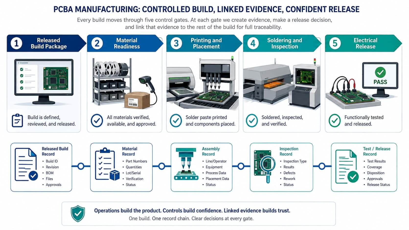
Evidence does not dictate what a customer must receive in terms of a delivery package. The level of detail or granularity of each record depends on the risk of the product, the contractual obligations of the parties, and the customer-specified quality plan. For example, one customer may require the supplier’s records to include lot-level data for each lot of PCBAs shipped, while another may require that each assembly’s serial number be linked to all material, process, inspection, test, and deviation records.
SPI (Solder Paste Inspection) and placement alarms are often viewed as providing a combined safety net, but they both provide no insight into the same class of failure. For example, if a component produces no placement alarm and is placed on an acceptable solder paste deposit, these records offer no protection against a cold joint that may result from insufficient time above liquidus for the thermal mass of the pad. Therefore, neither the SPI nor placement record will indicate that a failure exists due to this gap.
This risk is compounded for a double-sided assembly because the second-side reflow cycle changes the thermal history of the first side, which means that side-specific support and a second-pass thermal review are performed as independent checks rather than by repeating the first-side thermal checks.
What Can Inspection and Electrical Test Actually Prove?
While electrical tests and inspection each provide evidence for certain release decisions, their results have different applications depending on what is being accepted for release, the available access, and the acceptance criteria for each designated feature.
In its J-revision announcement, IPC separates the functions of J-STD-001J from those of IPC-A-610J. While J-STD-001J covers soldering process and material requirements, IPC-A-610J deals with the acceptability of completed assemblies. Both standards are often used together; however, visual acceptance does not verify electrical or functional capability.
The coverage of each ICT test also depends on the ICT test fixture interface. Connectivity among the probes, wiring, and test nodes in relation to test fixture verification is covered in Keysight’s guidance on ICT test fixture verification.
Therefore, the test plan should define all accessible nodes, fixture and program revisions, expected limits, and retained results. When selecting PCB assembly inspection and test methods, coverage, package visibility, access to test points, and product risk are to be considered.
How Should Deviations and Rework Be Controlled?
The control of a deviation is established when the affected configuration, approval authority, containment, action taken, reinspection results, and final disposition are recorded. Without this chain, repairs may have been technically acceptable; however, the company may be unable to establish the identity of the units affected or the validity of the evidence retained.
A compact exception workflow is:
- Stop all affected operations and segregate all materials that could potentially be affected.
- Identify the unit, lot, revision, process stage, and suspected scope.
- Document the nonconformance and obtain the appropriate technical disposition.
- Proceed only with the approved rework, repair, substitution, or process adjustment.
- Repeat all inspections and tests that have been made invalid by that action.
- Cross-link the disposition and new results to the affected unit or lot before release.
Whereas a design change alters the authorized product definition, a deviation allows a defined departure from that product definition. Rework takes an item back toward meeting the original requirements; repair allows the item to be restored to a usable condition but not necessarily to its original condition. The terminology and approval process for both terms are defined by the contract and the quality system in place.
An example of weak configuration control would be a company entering into an oral agreement with someone on the production line. The record must contain the name of the person approving the action, which items have been affected, and what previous evidence is to be reevaluated. If this does not occur, the final pass label may hide the fact that the technical decision is still open.
How Does Traceability Support Final PCBA Release?
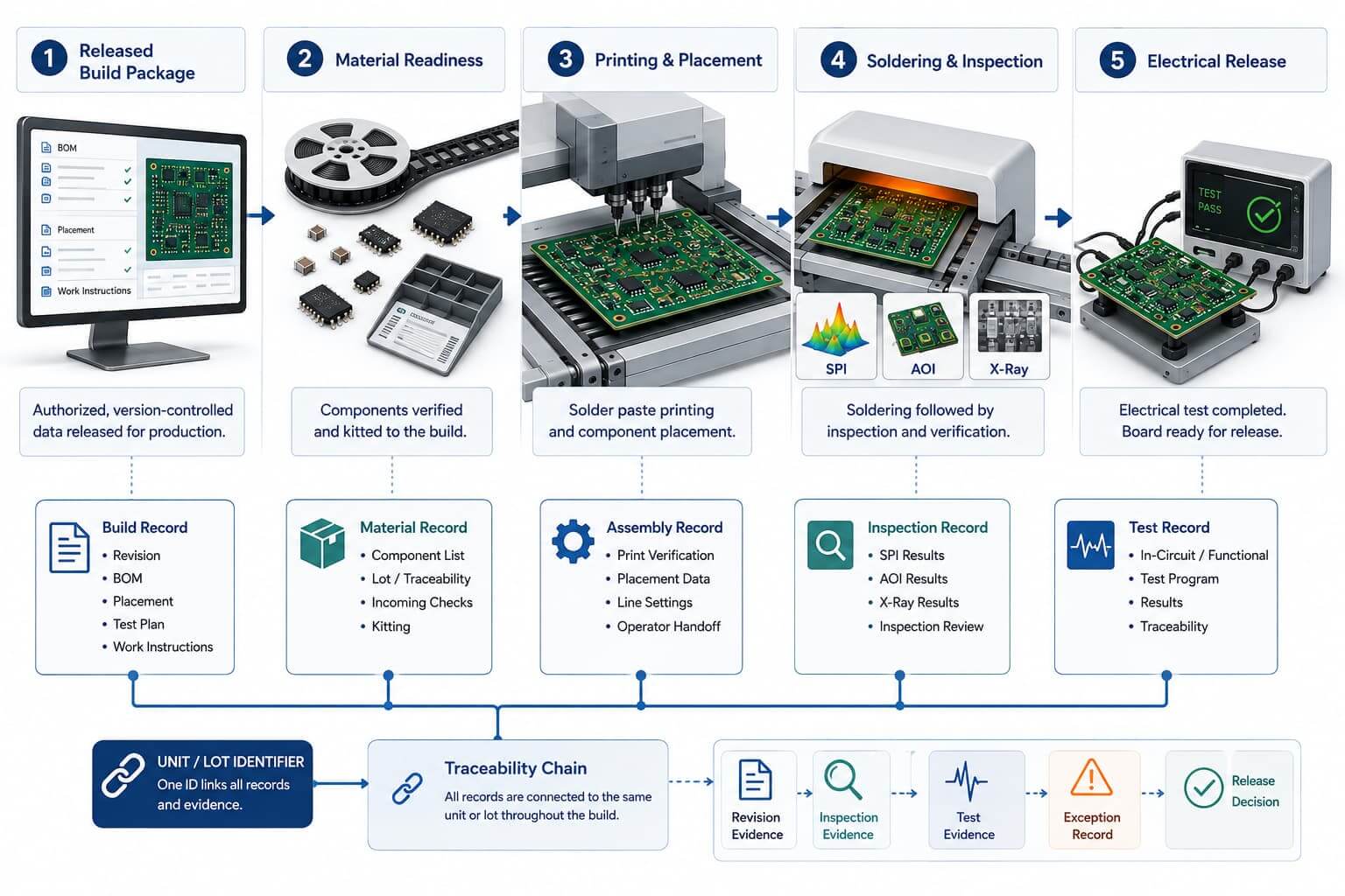
To determine how traceability is associated with the final release of PCB assemblies, you must establish a level of traceability deep enough to isolate the materials, process events, inspections, tests, and exceptions at the risk level agreed upon by the customer and supplier for traceability controls. You do not need to create a full genealogical tree for every project produced; instead, you need to confirm that the required genealogy can be established at the agreed traceability level.
IPC’s Factory of the Future overview describes IPC-1782 as a risk-based manufacturing and supply-chain traceability standard developed between the user and supplier. The IPC published revision history indicates that IPC-1782B is the most current available revision, while the IPC status page for IPC-1782C indicates that it is currently a working draft. The project should specify which released version of the IPC-1782 standard applies rather than expecting to use a draft requirement.
Depending on the traceability level approved between the user and supplier, the records that link the PCB assembly or production lot back to the released product and process revisions will reflect the following:
- Material identification, lot, and date-code information
- Tooling, program, equipment, or recipe events associated with the job
The same evidence chain may include inspection and testing results based on the approved acceptance requirements, as well as deviations, approved rework or repairs, repeated verification, and the final acceptance, hold, rejection, or release status.
Machine-to-system data may also be used to support this evidence chain. IPC-2591 Version 2.0 added messages for examples such as board-vendor identification, placement-cycle and failed-pickup events, and recipe changes. These examples demonstrate the connected manufacturing data that can be captured; however, they do not establish that a supplier has deployed IPC-CFX or is satisfying the customer’s traceability contract using only raw machine data.
A Practical PCBA Manufacturing Release Checklist
The final PCB assembly review checklist should be used to confirm that the PCB assembly has been built according to the intended configuration and authorized route, passed all defined checks, and closed all exceptions.
Configuration
Verify that the product, bare board, BOM, placement data, assembly drawing, firmware, and test-program revisions match those of the released job. Approved variants, no-fits, alternatives, and deviations should be visible to both production and inspection personnel.
Process
Verify that the executed route matches the board side, component-technology mix, thermal constraints, access requirements, and approved instructions. Tooling, programs, recipes, and material status must be identifiable at the approved traceability level, along with in-process checks conducted before later processes obscure the relevant features.
Verification
Verify that inspection has been conducted on all selected visible and concealed features of the PCB assembly using the defined inspection criteria. During electrical testing of PCB assemblies, each network or function exercised, method of access, firmware, limits, and result format must be identified. Electrical checks that failed or were interrupted must have an approved disposition, and a valid repeat test must be performed where needed.
Disposition
Verify that nonconformances, deviations, rework, and repair information have been linked to the affected PCB assemblies or lots, the responsible approval authority, and any repeated verification. The final acceptance, hold, rejection, or release status must be recorded at the agreed traceability level.
Making the decision to release a PCB assembly involves a judgment regarding the extent of the linkage between the records associated with the release of that assembly, not just the number of inspection stamps on each assembly. You must ensure that the finalized PCB assembly is based on the intended configuration, executed route, defined evidence, and closed exceptions before deciding whether to release it. Therefore, all of these traceability controls should be agreed upon and documented during the handoff of the PCB assembly service before manufacturing material is prepared and released for production.
Frequently Asked Questions
Q1. Which inspection and test results must be repeated after rework?
Any verification that has become questionable due to the approved rework must be repeated. This will include renewed verification of the component’s identity, polarity, placement, and solder joint. For work performed on components whose solder joints are concealed from view, X-ray verification may be required. Modified electrical networks, firmware, test access, or test methods may require in-circuit testing (ICT), flying-probe testing (FPT), or functional retesting. The disposition will list all affected assemblies, required verification checks, applicable limits, and details regarding the new verification results and their linkage to final release.
Q2. Does every PCBA need unit-level traceability?
No. IPC-1782B defines risk-based traceability levels for PCB assemblies. Traceability at the lot level may be all that is needed to perform one isolation task, whereas another product may require serial-level traceability to identify the material, process, test, and exception history for each PCB assembly. The required level of traceability should be established before the start of production and not derived retrospectively after an issue has occurred.
Q3. Can a prototype assembly process be reused for volume production?
Only after the route and controls required to verify that the assembly can be produced under the new conditions have been validated. Volume production may require different panel handling, component packaging, feeder setup, tooling, inspection programming, test fixtures, sampling, or record-retention requirements. The prototype shows that the defined configuration and verification passed for that prototype; it does not guarantee the correct operation of the assembly method under all subsequent production conditions.
Conclusion
Control of printed circuit board assembly (PCBA) manufacturing is established when the released data, executed operations, inspection and test evidence, and exception records verify that the correct PCB configuration has been produced. The connection between these items will prevent an established, capable line from producing the incorrect revision and will ensure that a pass result does not indicate something that the method did not actually verify.
References & Sources
- PCB Editor Documentation – KiCad
- Automating Generation of Outputs from Altium Designer – Altium
- IPC Releases J Revisions to Two Leading Standards for Electronics Assembly – IPC
- How to Verify ICT Fixture Integrity – Keysight
- Factory of the Future Program – IPC
- IPC Document Revision Table – IPC
- Status of Standardization – IPC
- IPC Releases Version 2.0 of IPC-2591 – IPC