Upload BOM & Gerber

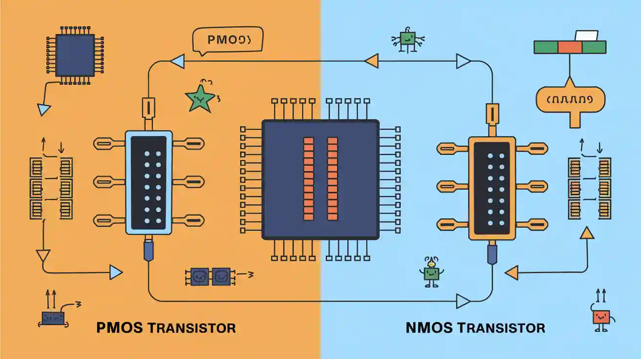
An individual MOSFET diagram does not always provide enough information by itself to determine whether it is classified as an NMOS or PMOS device. Determining the classification of an isolated MOSFET from the diagram depends on which diagramming convention is used, how the arrow is represented, whether the body terminal is visible, and whether the manufacturer or library identification has provided the type. For accurate determination of the device type, the process starts with the diagram representation and does not rely upon memorized arrow symbols.
- A four-terminal diagram will usually allow the device to be identified, while a three-terminal diagram without the arrow or body connection may not allow this determination.
- An enhancement-mode NMOS requires a positive VGS and an enhancement-mode PMOS requires a negative VGS, with the gate voltage referenced to the source voltage.
- N-channel vs. P-channel describes polarity; enhancement vs. depletion describes operating mode, and the channel line may indicate operating mode rather than polarity.
- The definition provided by the library and manufacturer’s datasheet takes precedence over the position, orientation, color, or a generic diagram from the internet for that device.
Contents
show
Can You Identify NMOS or PMOS from the Symbol Alone?
Sometimes it is possible to make that determination when the diagram contains a polarity cue whose meaning is known. For instance, a four-terminal diagram exhibiting a body terminal allows for verification of the P-to-N direction of the body-source junction. A source-arrow diagram allows for confirmation when its documentation specifies that the arrow represents conventional current. In simplified CMOS notation, the presence of a bubble on the gate usually identifies the P-channel pull-up device.
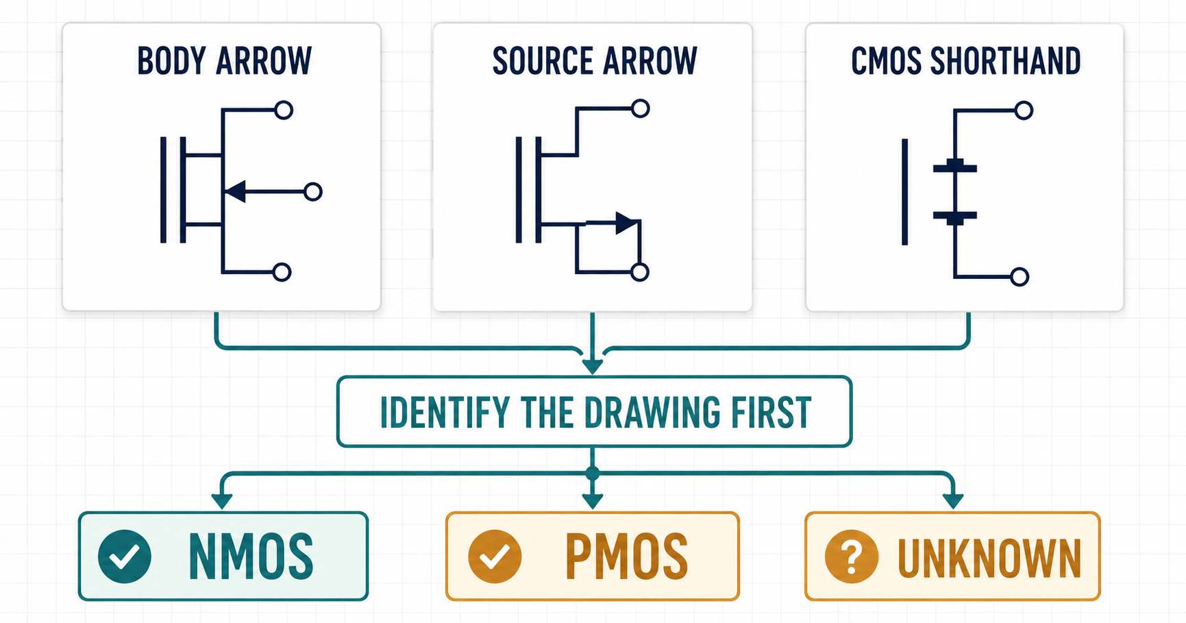
Images may be cropped to the point that the source and drain labels are not apparent, or the library used for the symbol may use an arrowless generic MOSFET symbol. As such, the only technically accurate response could be “not identifiable from this glyph.” In addition, rotating or mirroring the glyph does not change the device polarity, so statements such as “top is PMOS” and “bottom is NMOS” indicate only how the circuit has been drawn. After identifying the family of symbols, additional information may be present to reach a conclusion, but position alone cannot provide a definitive conclusion.
Why NMOS and PMOS Behave Differently
NMOS structure and turn-on
A typical enhancement-mode NMOS will have N-type source and drain regions and a P-type body. When VGS is close to 0 volts, no strong channel will exist connecting source to drain. Increasing the gate voltage above the source attracts electrons under the insulated gate. When VGS exceeds VGS(th), an N-type inversion channel will begin to form. Normal operation should be understood as electrons moving across the device from source to drain; however, conventional drain current is defined as flowing from drain to source. When someone writes about “current direction,” if the discussion does not clarify whether it means actual carrier movement or conventional current, the statement can be misleading.
PMOS structure and turn-on
The configuration of a typical enhancement-mode PMOS is the reverse of NMOS. The P-type source and drain regions are placed in an N-type material, such as the body or well. The PMOS will begin to conduct when the gate potential is lowered below the source, making VGS negative enough to allow the creation of a P-type channel. Holes are the majority carriers within the PMOS, and the movement of holes from source to drain corresponds to conventional current flowing from source to drain.
The voltage applied to the gate does not need to be negative relative to ground. It needs to be negative relative to the source of the PMOS device, making this distinction essential when a PMOS is used in high-side switch applications, where the PMOS source is at the positive supply voltage.
What the usual speed and resistance claim really means
In comparable silicon structures, the mobility of electrons is generally greater than the mobility of holes. As a result, for comparable silicon structures with similar geometry and bias, NMOS devices can provide higher current, faster switching capability, or lower RDS(on) than PMOS devices. This is a design tendency and does not mean this will hold true across all NMOS and PMOS devices.
NMOS and PMOS devices can vary significantly in voltage rating, die area, processing technology, gate charge, package resistance, temperature, and available gate drive, thus preventing a universal ranking of NMOS over PMOS. As such, it is inappropriate to claim that “NMOS devices are 2.5 times faster” without stating that this is process-specific information and cannot be considered a general MOSFET rule.
Which MOSFET Drawing Convention Are You Looking At?
Before interpreting an arrow, identify which symbol convention is being used and what the arrow represents.
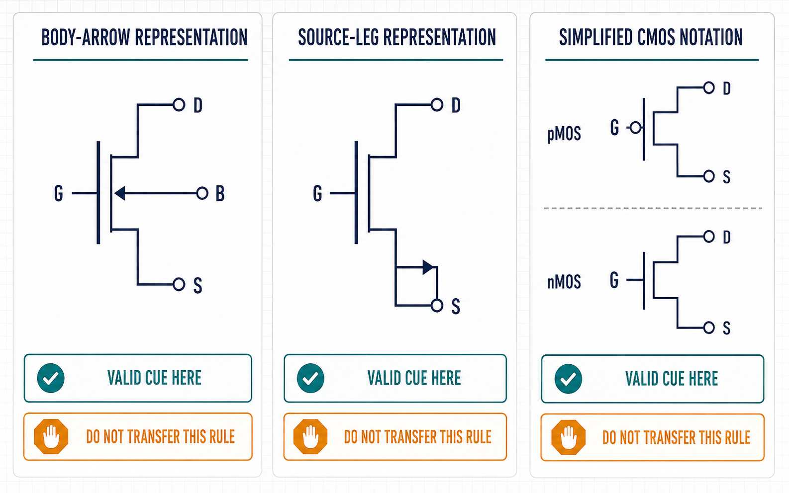
Body-arrow drawings
The arrow on a body drawing represents the P-to-N direction of the body-to-source PN junction. When the body and source are identified, this relationship can be used to determine whether the device is N-Channel or P-Channel. Therefore, if you have a body-arrow drawing and a source-leg-arrow drawing, do not attempt to use the same mnemonic for both drawings.
Body-arrow drawings show arrows pointing in opposite directions for the two channel types. These opposite directions represent the polarity of the body-to-source junction. Rotation, mirroring, or the side on which the body lead is drawn can change the apparent arrow direction without changing the device polarity; trace the arrow between the identified P and N regions instead.
Source-leg-arrow drawings
In contrast, a source-leg-arrow drawing places the arrow on the source terminal of the three-terminal device. In tools that define this arrow as conventional current direction, normal NMOS current enters the drain and leaves the source, while normal PMOS current enters the source and leaves the drain. Therefore, the meaning of the source-leg arrow should be confirmed from the tool or manufacturer’s symbol convention rather than from the physical position of the source terminal.
Simplified CMOS and arrowless drawings
In digital CMOS logic circuits, the body terminal and arrow are frequently omitted from the drawing; most often, a bubble on the gate identifies the active-low PMOS device, while the unbubbled device is NMOS. Bubbles are not universal polarity markers; therefore, a bubble should be interpreted according to the convention used in that logic diagram. An arrowless generic three-terminal drawing only indicates the gate, drain, and source terminals; therefore, unless additional identification information, pin labels, or library metadata are present to indicate polarity, it is not safe to guess.
In a MOSFET drawing, the insulated gate is separated from the channel; however, a JFET gate meets the channel junction. Thus, while library stylization may differ, the physical separation between the insulated gate and the channel can be used as a family cue, but the exact part definition should still be verified.
Does the Channel Line Show N-Channel or P-Channel?
No. Continuous, broken, or omitted channel lines are often used to differentiate depletion mode, enhancement mode, or simplified drawing styles and should not be taken to mean that the channel is automatically labelled N or P.
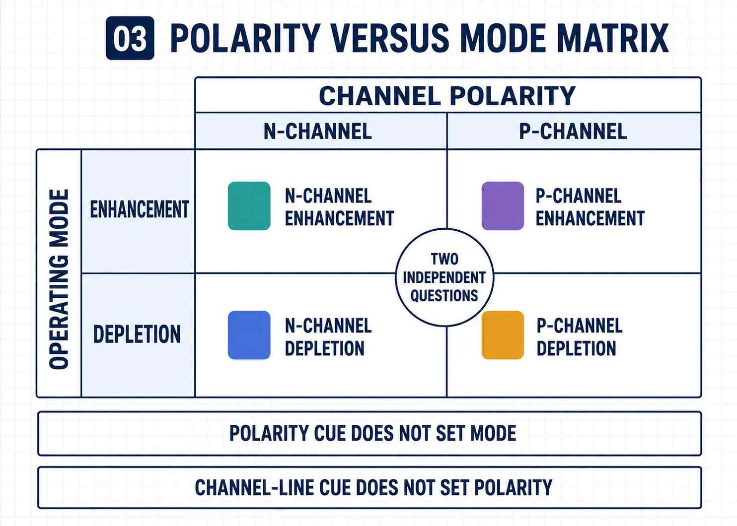
Most examples of switching devices utilize enhancement-mode devices, which are normally off when VGS is approximately 0 V. In contrast, depletion-mode MOSFETs will conduct when VGS is approximately 0 V, requiring the opposite gate bias to reduce the channel current. The line that represents a channel will only be useful when you have already referred to a standard drawing for the meaning of that line or to the component definition.
How Circuit Context Can Confirm—But Not Define—the Symbol
CMOS inverter
In a basic enhancement-mode CMOS inverter, the PMOS source is connected to VDD, the NMOS source is connected to ground, the drains are tied together at the output, and both gates are driven by the same input. With a low input, the PMOS has a sufficiently negative VGS to turn on; the NMOS has an approximate VGS of 0 V, causing it to be in a “turned off” state, thus causing the output to go high.
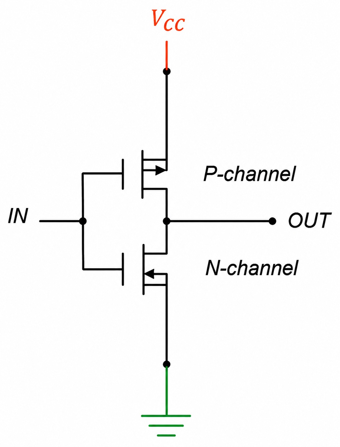
Conversely, with a high input, the NMOS will be in an “on” state, and the PMOS gate will approach the same potential as its source, thus preventing it from conducting and causing the output to go low. However, this does not provide a definitive determination of the polarity of an isolated, cropped glyph; the shorthand notation used to represent these devices assumes that they are enhancement-mode CMOS devices.
Low-side NMOS and high-side PMOS switching
Because the NMOS source can sit near ground, it is generally well suited for use as a low-side switch. In addition, a PMOS is commonly used on the high side at reasonably low supply voltages because pulling its gate below its source creates the required negative VGS without needing a bootstrapped high-side driver. A disadvantage of this approach is the fact that PMOS devices tend to have higher RDS(on) when compared with NMOS devices of similar ratings.
The switch position itself provides further supportive evidence, although rotated symbols, half bridges, transmission gates, source followers, and custom libraries all break the basic top/bottom mnemonic. For discrete devices, the body diode can provide additional corroborative evidence, provided the terminal mapping has already been established by reliable means; the anode of the body diode for NMOS is connected to the source and the cathode is connected to the drain; the reverse is true for PMOS.
What Should You Check When the Symbol Is Ambiguous?
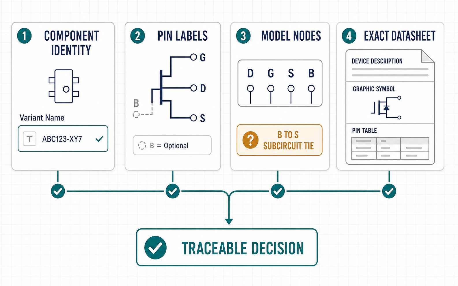
Use the strongest source of evidence available and stop when that source does not support a more specific conclusion. The most useful sources and their possible limitations are:
- Examine the component identity. Open the complete library record or symbol and write down the part number, MOSFET type, and all aliases that exist.
- Compare manufacturer data. Use the same ordering code to locate the device description, device graphic symbol, package variant, and pin table for comparison.
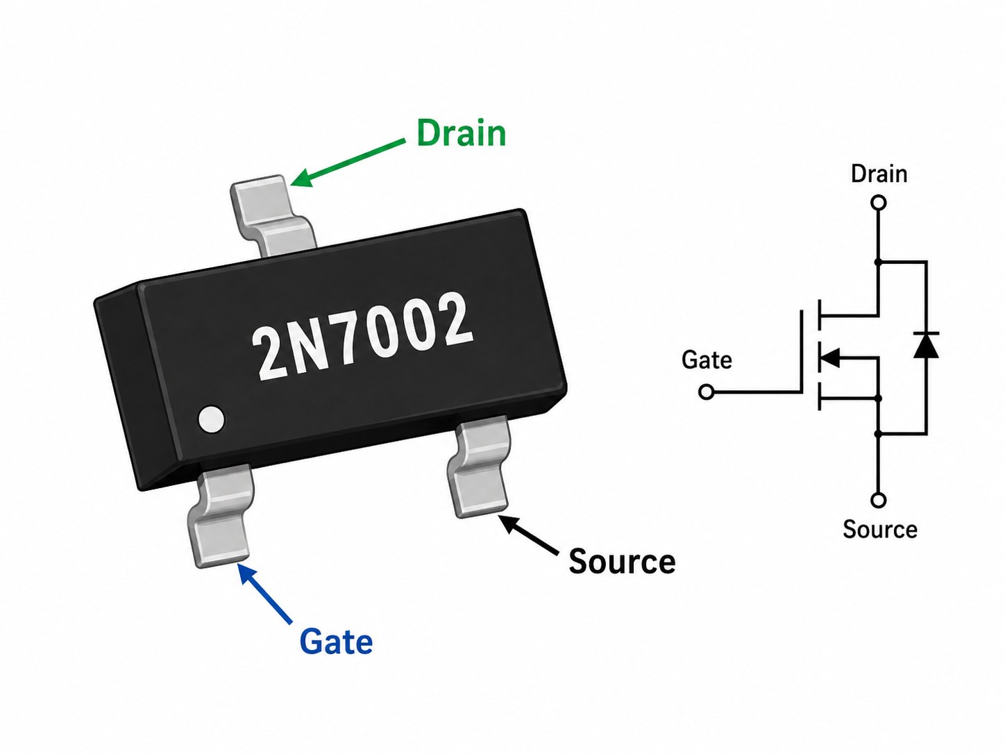
- Detect terminal & body connection. Check that G, D, S, & B on the symbol, footprint mapping, and model nodes are verified and correct. Do not assume that all SOT23 MOSFETs will have the same pin-out configuration as depicted.
- Once you know the representation, interpret the arrow, bubble, or channel line. If you do not see sufficient evidence, record the polarity as indeterminate, not based on circuit positioning folklore.
Use VGS as a Sanity Check, Not the First Clue
For both types of devices, VGS = VG − VS. An enhancement-mode NMOS begins to conduct when VGS is sufficiently positive. An enhancement-mode PMOS begins to conduct once VGS is sufficiently negative. This check of polarity can expose an incorrect interpretation in a complete circuit layout, but cannot determine source polarity if the source terminal is unknown.
2N7002: a verified NMOS example
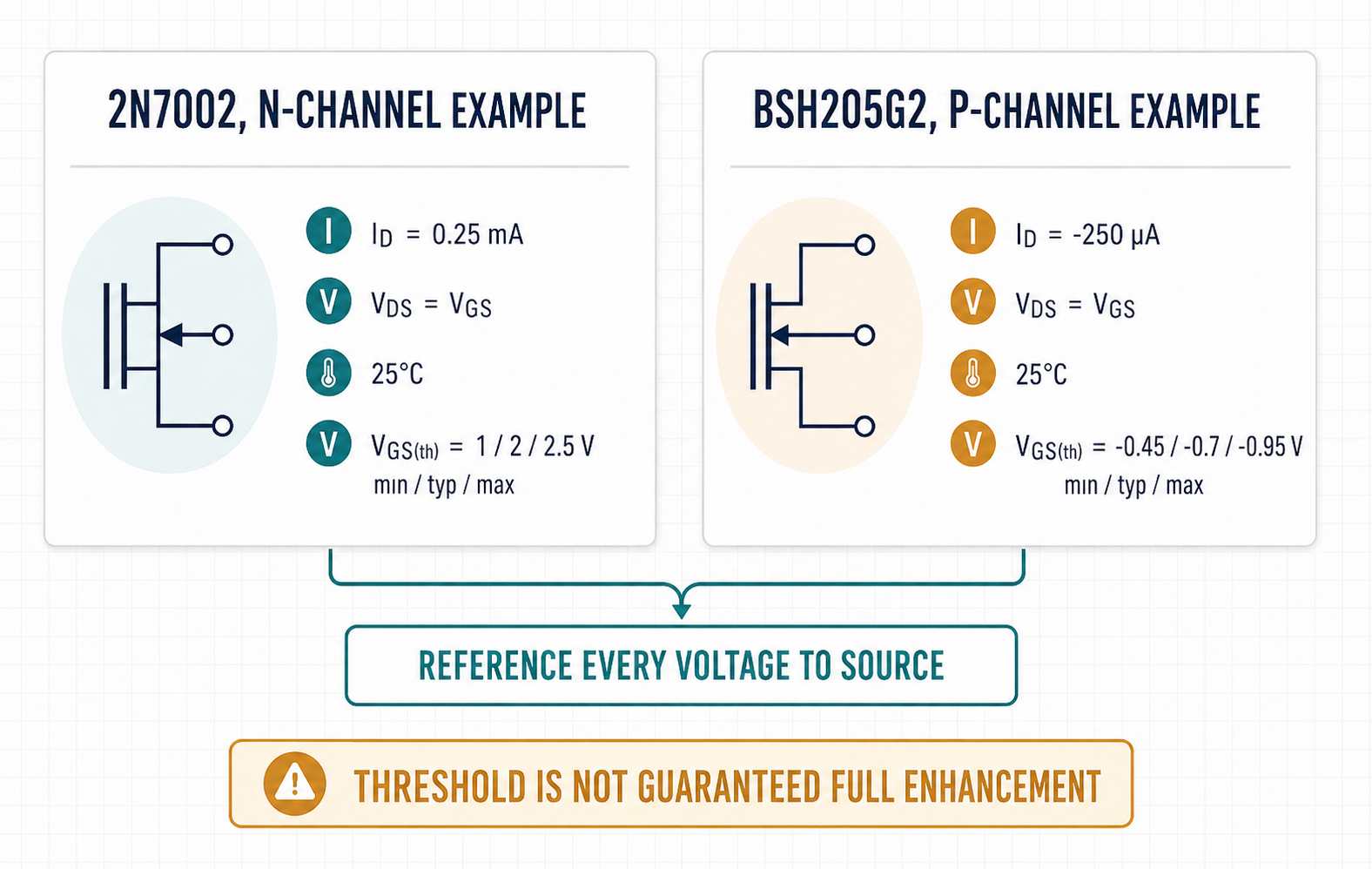
According to Nexperia, the 2N7002 is a 60 V, 300 mA N-channel enhancement-mode Trench MOSFET. In its SOT23 package configuration, Pin 1 is Gate, Pin 2 is Source, and Pin 3 is Drain. At 25 °C, with ID = 0.25 mA and VDS = VGS, the VGS(th) values are 1 V minimum, 2 V typical, and 2.5 V maximum. These values confirm the positive NMOS threshold sign and show why the test condition matters, as the device is only beginning to conduct at 0.25 mA.
BSH205G2: a verified PMOS example
According to Nexperia, the BSH205G2 is a −20 V P-channel enhancement-mode Trench MOSFET.
The terminal assignment in the SOT23 package of the BSH205G2 is 1 = Gate, 2 = Source, and 3 = Drain, as with the NMOS transistor above; however, this is only true for these two examples, and the terminal assignment for the SOT23 package is not universally applicable.
The VGS(th) specification for the BSH205G2 states a minimum measurement of −0.45 V, a typical measurement of −0.7 V, and a maximum measurement of −0.95 V at 25 °C, with ID = −250 µA and VDS = VGS. The numerical order of the specification can appear counterintuitive because progressively more negative values are numerically smaller. Preserving the minimum, typical, and maximum assignments will prevent an incorrect interpretation of the specifications due to mislabeling or misreading.
Threshold voltage marks the onset of a small specified drain current; it is not the point at which the MOSFET reaches its guaranteed low RDS(on), and it should not be treated as a recommended VGS drive level. RDS(on) specifies how well the MOSFET will conduct under the stated VGS conditions, while gate charge, current, temperature, power dissipation, and SOA limits must also be considered for the selected MOSFET.
Conclusion
When reading both PMOS and NMOS devices at the same time, the proper sequence is first determining the correct symbol convention and terminal assignment on the device, then determining the individual configuration of each MOSFET from the datasheet according to how the symbols are assigned and checking that result against VGS behavior. When the decisive polarity cue is absent, keep the result indeterminate rather than using circuit position as proof.
References & Sources
- Graphical symbols for diagrams – IEC 60617:2026 DB
- Graphic Symbols for Electrical and Electronics Diagrams – IEEE/ANSI 315-1975
- NMOS and PMOS Symbols – National Instruments
- Avoid Common Mistakes When Selecting and Designing With Power MOSFETs – Texas Instruments
- 2N7002 product data sheet – Nexperia
- BSH205G2 product data sheet – Nexperia
- What is a MOSFET? – Infineon
- Transistor_FET symbol library – KiCad
- MOS Transistors – Stanford EE100
- Depletion MOSFET VS Enhancement MOSFET explained, N-channel MOSFET & P-channel MOSFET symbols – Electronics Repair Basics_ERB