Upload BOM & Gerber

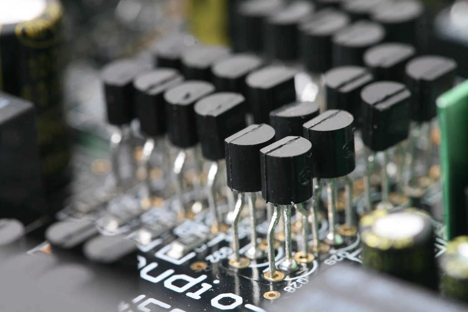
A transistor symbol represents the electrical device family through a schematic, along with the logical terminals and schematic connections of each terminal. The physical package and universal lead order are not included. The distinction between transistor types (BJT, JFET, MOSFET, and IGBT) is important because their symbols use different terminal names and visual cues.
To locate the family of the device, first identify the transistor family, locate the family-specific control terminal, and interpret the directional indicator (arrow or channel) associated with that terminal. Then trace the connected nets in the schematic. Once this information is available, the component layout should be matched to the footprint pad layout of each terminal in the symbol before the design is committed to copper. Only when all symbols have been appropriately matched to all footprint pads can complex library checks be progressed into formal PCB design and library verification.
Contents
show
What Does a Transistor Symbol Actually Show?
A generic symbol shows the logical device type, the terminals connected to the logical device, and some level of logical connectivity. However, a generic symbol does not indicate whether the logical device has a certain package shape, voltage rating, operating state, or sequential order of physical leads.
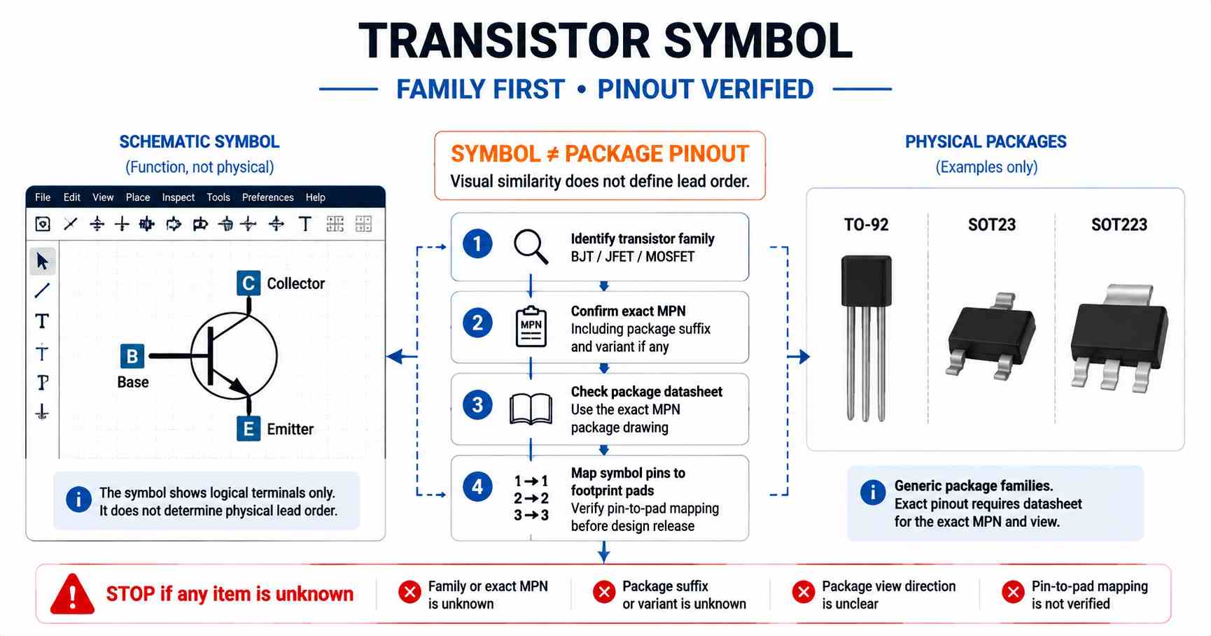
For instance, the BJT uses base, collector, and emitter as its terminals, whereas the FET uses gate, drain, and source as its terminals. This is important because the pin numbers and functional connections of BJT and FET terminals are determined by different symbol conventions.
In addition, while the circuit being designed and implemented with a schematic will generally show how components are interconnected, it does not provide information about how the components are actually operating, such as bias, gain, current limit, or operating region. Therefore, proper operation cannot be assumed from the symbol alone. Component values, possible net conditions, and actual device specifications must be referenced to ensure proper operation.
Because of the large number of different library symbols that can represent the same functional device with different pin-number arrangements, transistor mapping can be considered risky.
Find the Transistor Family Before Reading the Arrow
To minimize risk, the best course is to first determine the transistor family by determining the direction of the control terminal and the routing of the current path. Only after identifying the component family should you attempt to interpret the directional indicator (arrow).

KiCad uses a logical library structure and therefore separates its symbol libraries into specific family categories (such as BJT, FET, and other device families), reducing the chance of using an incorrect library symbol for a design.
JFET and MOSFET symbols have different functions from BJTs; however, instead of a base, these devices use a gate. As previously stated, the drain and source terminals are connected through a channel, but the configuration of the gate, channel, body, and arrows will vary for each family of MOSFETs and JFETs depending on how the symbol has been drawn. For example, a power MOSFET may show a body diode or a source-body connection. The Nexperia MOSFET and GaN FET Application Handbook provides examples of these components, including a power NMOS example.
N-channel, P-channel, and enhancement/depletion modes are some characteristics that can be identified. The insulated gate separation of a MOSFET is one of the methods used to identify a MOSFET; JFETs use a gate junction to provide access to the channel rather than an insulated gate. Many libraries use a continuous channel for depletion mode and an interrupted channel for enhancement mode, although the arrangement varies depending on how the channel, body, and arrows are drawn. To confirm the definition of an unfamiliar symbol, check its controlled library definition instead of applying a mnemonic for identification.
The IGBT symbol has an insulated gate, like typical MOSFETs, and uses collector and emitter terminals for the output path. Do not rename the output terminals as drain or source, nor should the emitter arrow mnemonic be applied to the insulated gate; treat the gate as a family identification feature.
A number of symbols that indicate variations of a single family have been created using different modifications. Examples include Darlington pairs that combine multiple BJT stages, phototransistors that include arrows indicating incoming light, and multi-emitter devices that have multiple branches. The UJT symbol has three terminals: E, B1, and B2.
IEC 60617 is the official database for graphical symbols and is maintained by the International Electrotechnical Commission (IEC). IEEE/ANSI 315-1975 is an old standard and is currently Inactive and Reserved, but there is not necessarily a common identifier or numerical system in a given project.
How Do You Identify the Emitter, Base, and Collector?
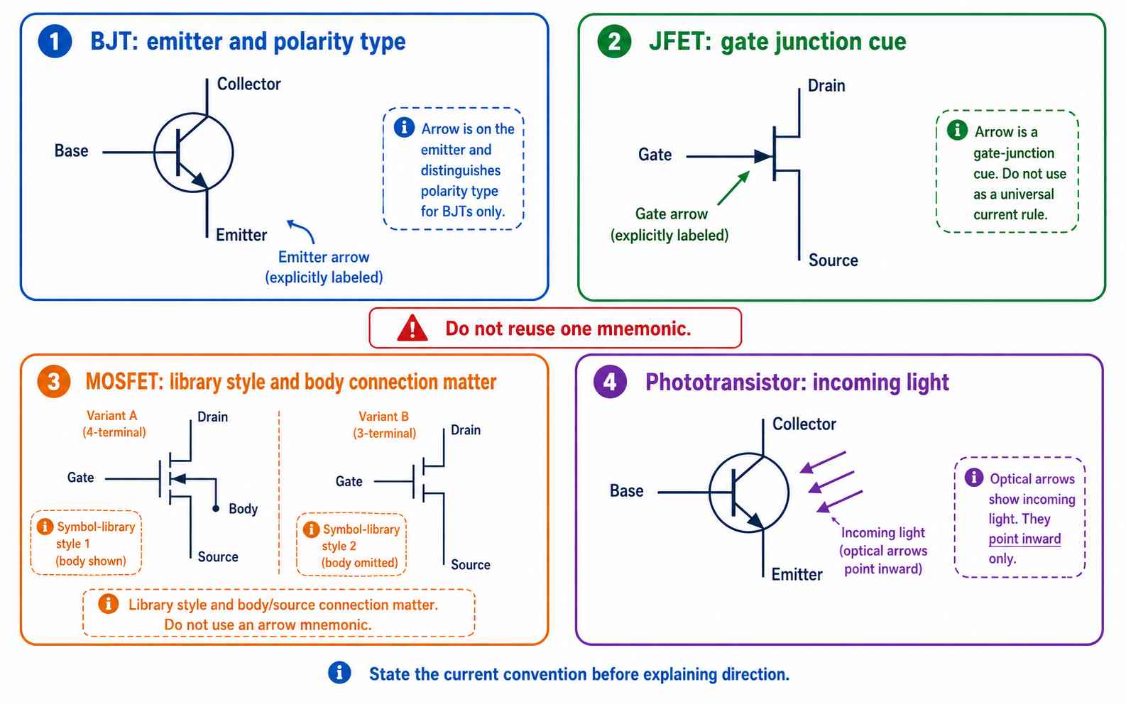
For a BJT (bipolar junction transistor) symbol, the arrow indicates the emitter. The base is connected to the middle base line, and the remaining main branch is the collector. BJT emitter arrows point outward for NPNs and inward for PNPs (refer to Analog Devices Chapter 8 for further clarification); this arrow rule applies only to BJT symbols.
The mnemonic NPN stands for “Not Pointing iN.”
Page position does not affect the terminal definition. A collector can be above, below, left, or right of the position shown. When a designer rotates the symbol, the collector can be positioned where needed. MIT’s teaching note about BJTs states that vertical and inverted configurations are drawing representations of the same device and do not represent different devices.
Some drawings of BJTs show a circle around them, and some do not. This circle does not change between NPN and PNP. The bipolar transistor reference found at All About Circuits shows circled and uncircled versions of BJTs, as well as multi-emitter versions.
If your scan does not show the arrow, look for the trace label and net. After that, refer back to the schematic legend or source library. You should never assume the missing terminal’s location from the position on the page.
Can You Read the Same Symbol After It Rotates?
Yes. Although rotating a transistor symbol may change its position on the page, it does not change the topology of the device. The control terminal will still connect to the same device structure; the emitter will still have an emitter arrow; and all labeled pins will continue to connect to the same net.
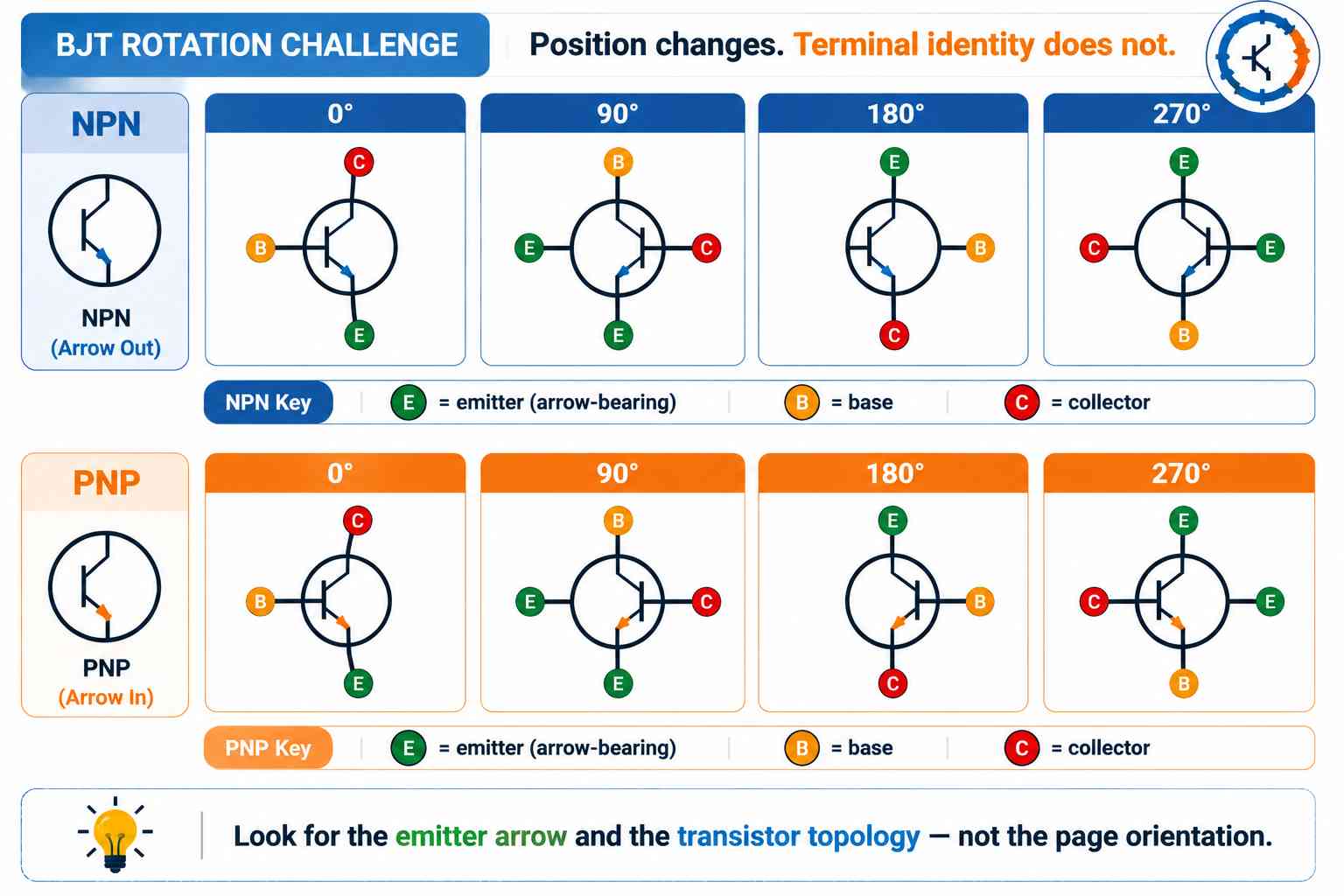
Make sure to confirm the following items on every transistor symbol that has been rotated:
- Identify which device family it belongs to. Determine if it is a BJT, JFET, MOSFET, IGBT, or a variant.
- Locate the control terminal. To identify the base or gate, the internal structure of the part should be used, not the screen location.
- For a BJT, the emitter arrow should be located and an identification made of whether it is an NPN or PNP type transistor.
- Trace the labels and nets. You can confirm the result by following the terminal names, pin numbers, and connected nets.
When mirroring a graphic, greater care should be taken than when rotating the graphic, due to the possibility that a CAD operation will only change how the symbol looks but not the identity of its pins if copied or redrawn from a legacy schematic. In addition, if the library definition and pin numbers for a graphic are not accessible, no attempt to duplicate the mapping can be made. The visual resemblance is not sufficient to create a map that can be released with quality.
Why Does One Arrow Rule Fail Across Transistor Families?
Arrows for BJTs show the emitter, arrows for JFETs correspond to their gate junctions. For MOSFETs, arrows indicate the body/source representation, while arrows for phototransistors indicate incoming light.
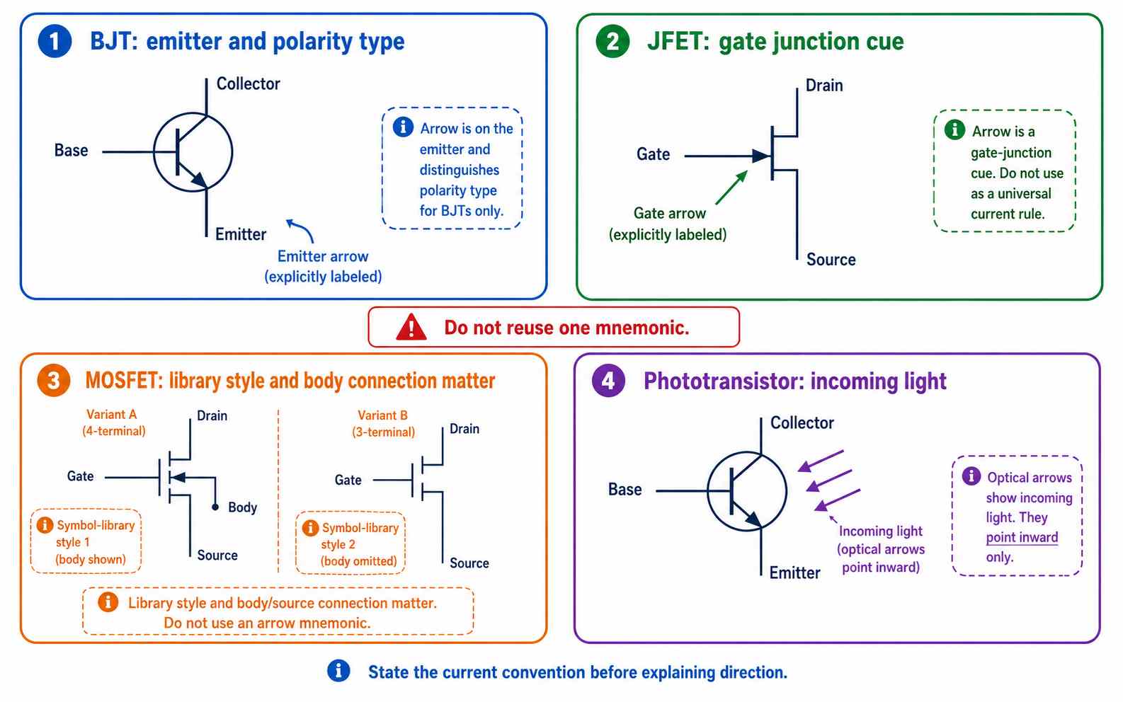
The direction of conventional current is the direction in which positive charge would travel. In metal conductors, electrons flow in the opposite direction (OpenStax College Physics, 20.1 Current). In semiconductors, current may consist of both holes and electrons, making it unsafe to summarize that “the arrow represents the flow of electrons.”
Using the arrow rule: “NPN out, PNP in,” should be reserved for the identification of BJTs and locating an emitter. For all other types of JFETs, MOSFETs, IGBTs, and light-related types, interpret arrows according to the symbols of the family and the exact library style used.
A detailed NMOS power symbol exposes the connections of the body, while a simple three-terminal device hides the body diode from view. Both device types can be used as abstractions for a common design, but they cannot be used to compare identical representations.
Phototransistors do not have the same function as standard transistors. Phototransistor arrows indicate the direction of incoming light, not the terminals of phototransistors. To see the arrows for LEDs, please refer to the article about LEDs as an optical device where the arrows represent the optical direction separately from the transistor terminals.
How Do You Read a Transistor Symbol in Circuit Context?
Picture an NPN transistor that is used as a low-side switch. The control signal for the transistor is connected to the base terminal, the emitter is connected to a reference point (often ground), and the collector connects to the load. This configuration suggests that the transistor is switching the load on and off, as in the Analog Devices BJT Switching example, but this does not confirm (prove) saturation, base-drive margin, or load-current suitability. Saturation, base-drive margin, and load-current suitability will depend on the values within the surrounding circuits, the voltages at each node of the circuit, and the individual transistor being used.
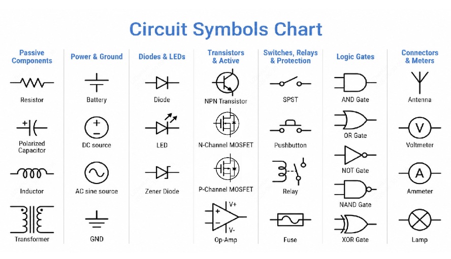
For a MOSFET load switch, trace the path of the controller (or driver) to the gate and trace the pathways for source and drain through the supply and load. The connection patterns may suggest whether the transistor is to be used as a high-side or low-side switch, but the orientation of the symbol does not define which physical pins to use or whether those pin numbers match the electrical requirements. Therefore, verify the actual G/S/D mapping between the electrical symbol and the package pinout in the device datasheet, together with the applicable voltage/current limits.
From Symbol Terminal to Package Pin
The connection of a logical terminal as a physical terminal occurs when the pin number listed in the logical symbol matches the pad number of the footprint and the package drawing. “Mapping symbol pins to footprint pads” is the procedure that KiCad Schematic Editor 10.0 documentation captures.
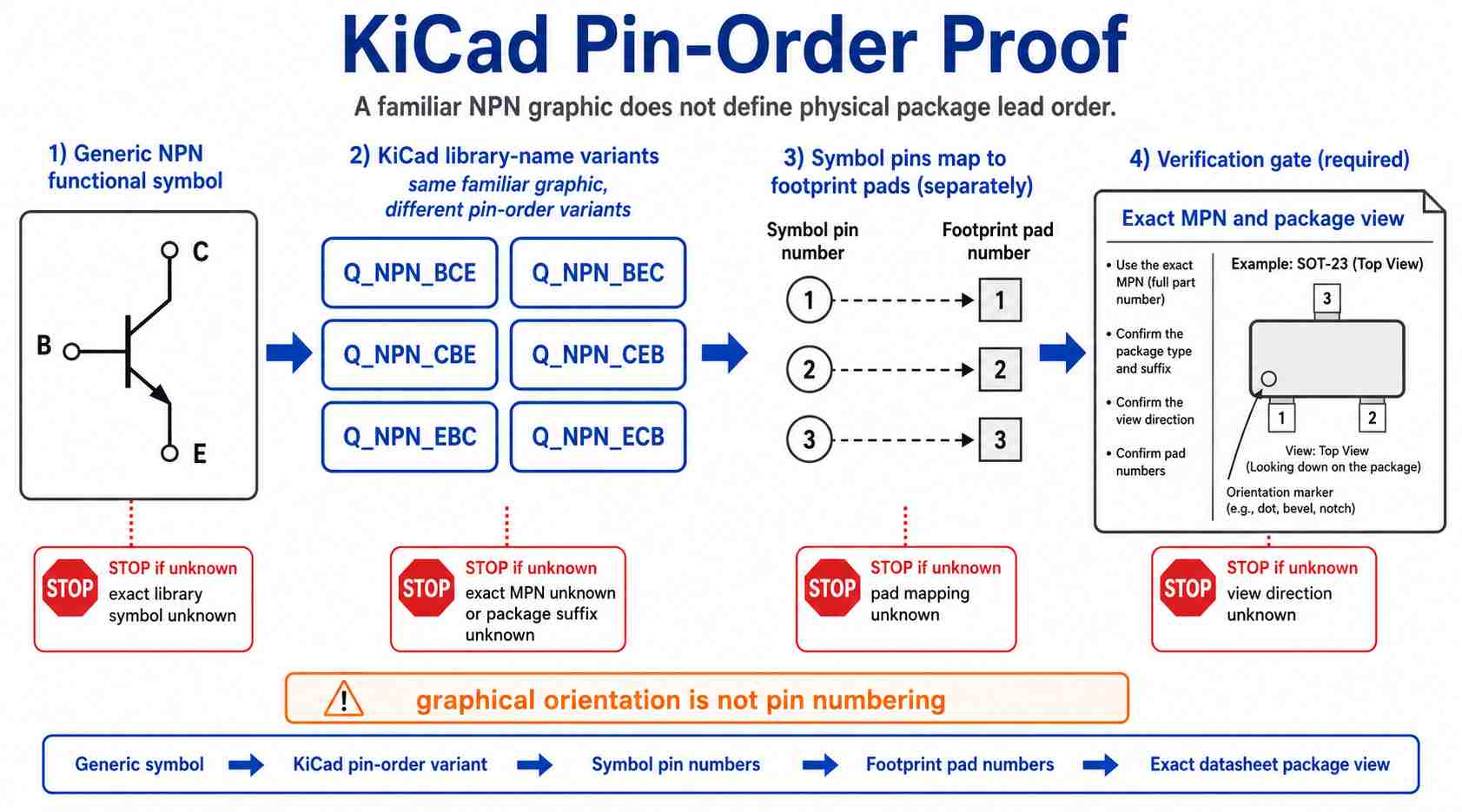
To understand how KiCad’s official BJT library represents the risks of using a generic NPN entry, we can compare the generic NPN terminal drawings to see that they are available in the six pin-order definitions: Q_NPN_BCE, Q_NPN_BEC, Q_NPN_CBE, Q_NPN_CEB, Q_NPN_EBC, and Q_NPN_ECB. They represent a total of six different configurations, all having the same functional identity. Before assuming the mapping for all six configurations is correct, you must run each of the following checks:
- Confirm the family by recording the transistor type as BJT, JFET, MOSFET, IGBT, or another specialized type.
- Open the exact library symbol and compare the terminal names to the pin numbers displayed.
- Inspect the assigned footprint.
- Match the symbol pin number to the corresponding pad number.
- Confirm the complete MPN by including the manufacturer’s name and package suffix.
- Open the package display to see the views of the top of the component, the bottom of the component, the component view, and the soldered component.
- Compare each of your released artifacts with each other. Make sure all the pads, symbol pins, package leads, and assembly orientation match.
If you find a check without direct evidence, stop immediately. An internet image or the family name of a package is not a substitute for the missing documentation for the given device. The PCB layout will preserve the schematic connectivity it receives, and it is not able to fix a logical error in a library’s mapping by itself.
Example datasheets illustrate the problems with making assumptions based on broad standards. An example is the Nexperia BCP54 series SOT223 datasheet that specifies pins 1, 2, 3, and 4 for B, C, E, and C, respectively. In contrast, the PMV16UN SOT23 device datasheet specifies that pins 1, 2, and 3 are G, S, and D, respectively. The mapping of these pin numbers is only associated with that specific manufacturer series and package view.
A schematic symbol cannot indicate whether or not a physical transistor has been damaged, is counterfeit, or is accurately described based solely on the appearance of the device.
To conduct device-health tests on an electronic circuit, the correct part with a defined measurement protocol, safe measurement method, and circuit conditions must be known.
Frequently Asked Questions
Q1. Is a MOSFET a type of transistor?
Yes. A MOSFET is a metal-oxide-semiconductor field-effect transistor. Its schematic description includes a gate, drain, and source (some symbols show a body connection or indicate it as part of the overall device). Please do not designate those same terminals as base, collector, or emitter, since those are names from the BJT family.
Q2. Why Do Some Transistor Symbols Have a Circle?
The circle is a drawing or library convention, not a universal physical-package outline. The BJT symbol may or may not include a circle, but you will still use the emitter arrow to determine the type (NPN or PNP). If the circle around a device is unfamiliar and the symbolism is more complex, please refer to the legend or symbol guide.
Q3. Can a transistor symbol be used to indicate that the part is not working properly?
No. A transistor symbol only indicates the type and wiring of the part; it does not indicate that the part is malfunctioning or has failed. Testing requires the exact part type and package, along with the circuit state and safe measurement method. A generic diode test mode does not provide enough accuracy for part qualification.
Q4. Do multi-transistor arrays use a different kind of symbol?
Typically, in electronic schematic symbols, arrays will be shown as a number of transistors in multiple units, each sharing a common physical package reference, as opposed to showing each transistor as a separate device with extra leads. Each transistor within an array will still have its own logical terminals and package pin assignments. Verify the specific library unit or the datasheet pin group before deciding how to assign the footprint, particularly for matched pairs or multi-transistor packages.
Conclusion
When reading a transistor symbol, establish the family prior to looking at the arrow. Locate the controlling terminal using only the visual rules designated for that family and maintain the topology when reading through rotation. The reading is only complete when it has been verified that the logical terminal being read agrees with the physical part documentation.
References & Sources
- IEC 60617 – Graphical Symbols for Diagrams – International Electrotechnical Commission
- IEEE/ANSI 315-1975 – IEEE Standards Association
- Chapter 8: Transistors – Analog Devices
- BJTs without tears – Massachusetts Institute of Technology
- 20.1 Current – College Physics – OpenStax
- Schematic Editor 10.0 – KiCad
- Transistor_BJT.kicad_symdir – KiCad
- sym-lib-table – KiCad
- 45 V, 1 A NPN Medium Power Transistors – Nexperia
- PMV16UN 20 V, 5.8 A N-channel Trench MOSFET – NXP Semiconductors
- MOSFET & GaN FET Application Handbook – Nexperia
- Transistors, Bipolar – All About Circuits
- BJT device as a switch – Analog Devices
- Transistor Explained in 6 Minutes: Animations and Visualisation – ConceptMotion