Upload BOM & Gerber

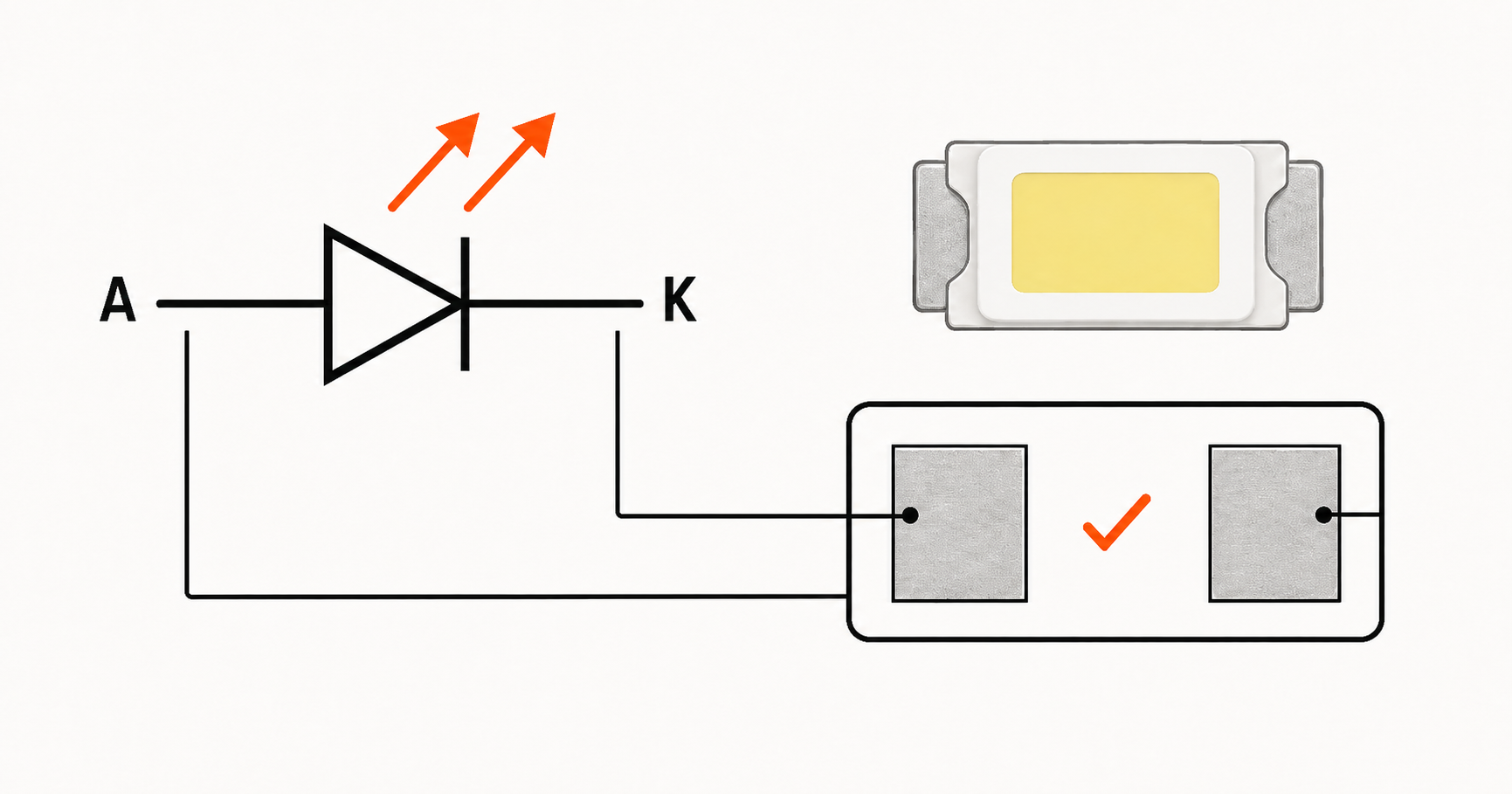
The outward arrows identify a light-emitting diode, but correct PCB polarity depends on more than recognizing the graphic. The symbol pins, footprint pads, package marking, and assembly orientation must all preserve the same anode and cathode identity.
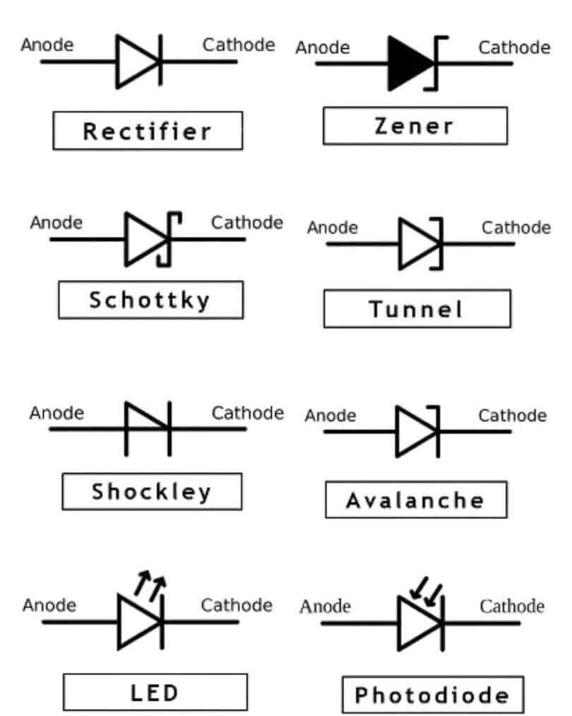
- • Two arrows pointing outward distinguish an LED from an ordinary diode and from a photodiode, whose arrows point inward.
- • The cathode bar identifies K. Screen position, symbol rotation, and pin numbering are not universal polarity rules.
- • The LED symbol does not specify forward voltage, operating current, color, package, thermal limits, or resistor value.
- • A safe PCB release preserves A/K identity from symbol pin to numbered pad, exact package marking, and placement orientation.
Contents
show
What Does the LED Symbol Mean?
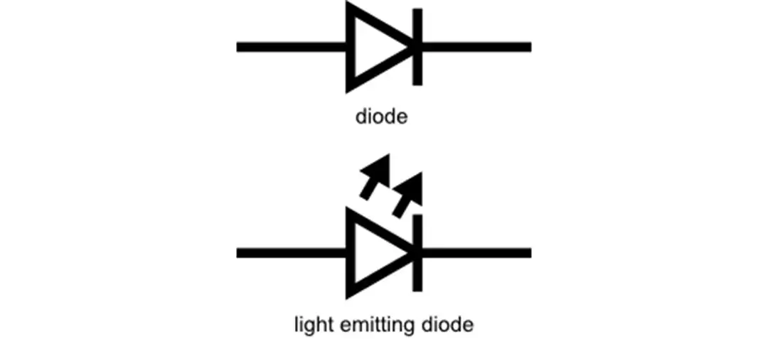
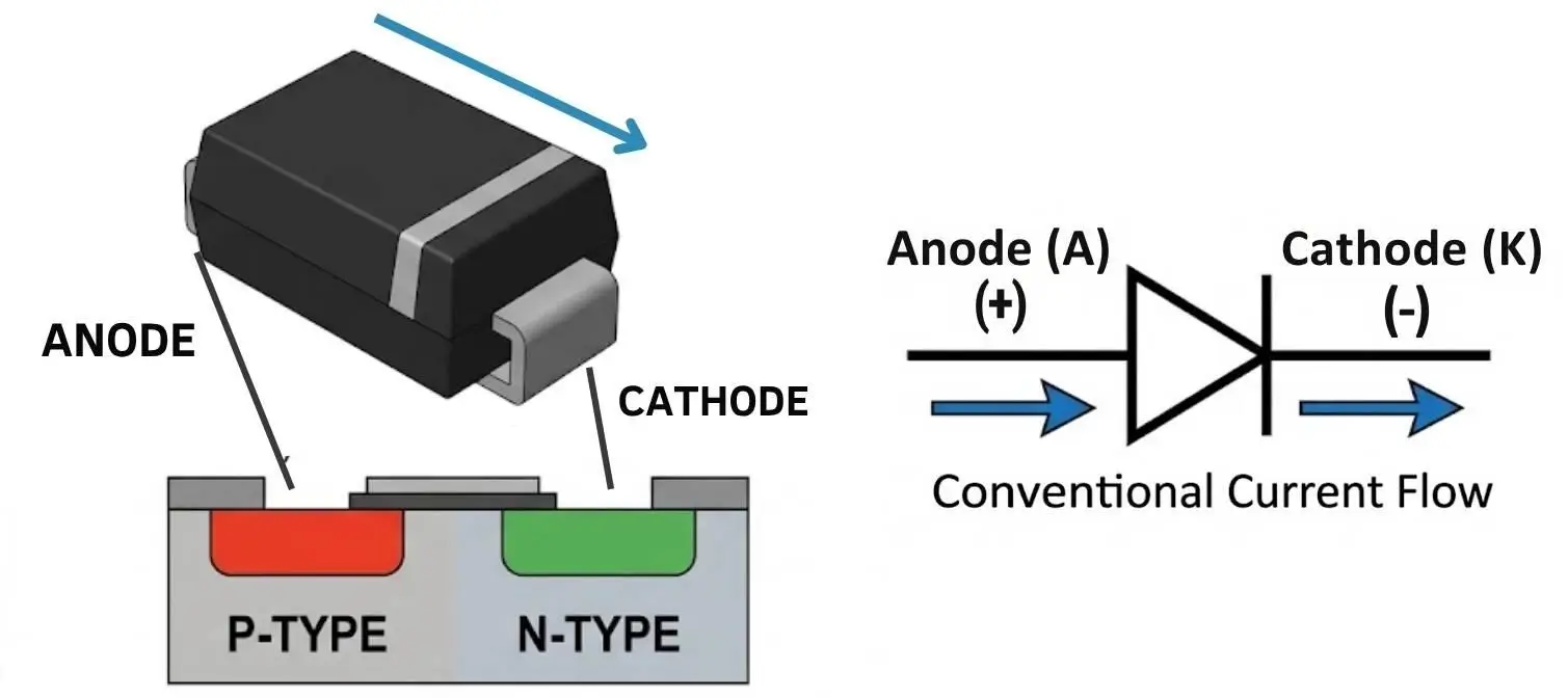
The LED symbol is similar to a diode symbol but features two arrows pointing away from the diode body to signify that light is leaving the semiconductor junction, not the direction of conventional current. The short bar on one side of the diode body indicates the cathode (K), while the other terminal is the anode (A).
In some drawings, part of the diode body may appear triangular; however, this shape does not represent a current arrow. The key elements of the LED symbol are the diode body, the cathode bar, and the two arrows indicating light emitted from the junction. The international standard IEC 60617 defines the family of graphical symbols used in diagrams. CAD libraries implement these standards by providing reusable electronic symbol files.
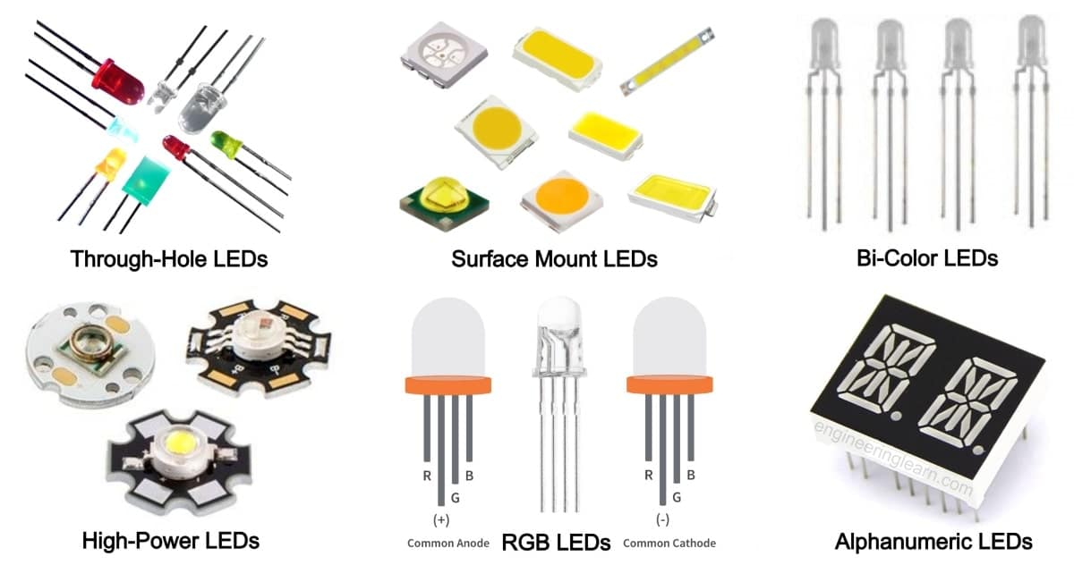
The LED symbol represents the electrical function of the device, not its physical appearance. It does not provide information on whether the part is a 3 mm through-hole LED, a 0603 chip LED, a six-lead RGB package, or an addressable lighting module.
How Do LED, Diode and Photodiode Symbols Differ?
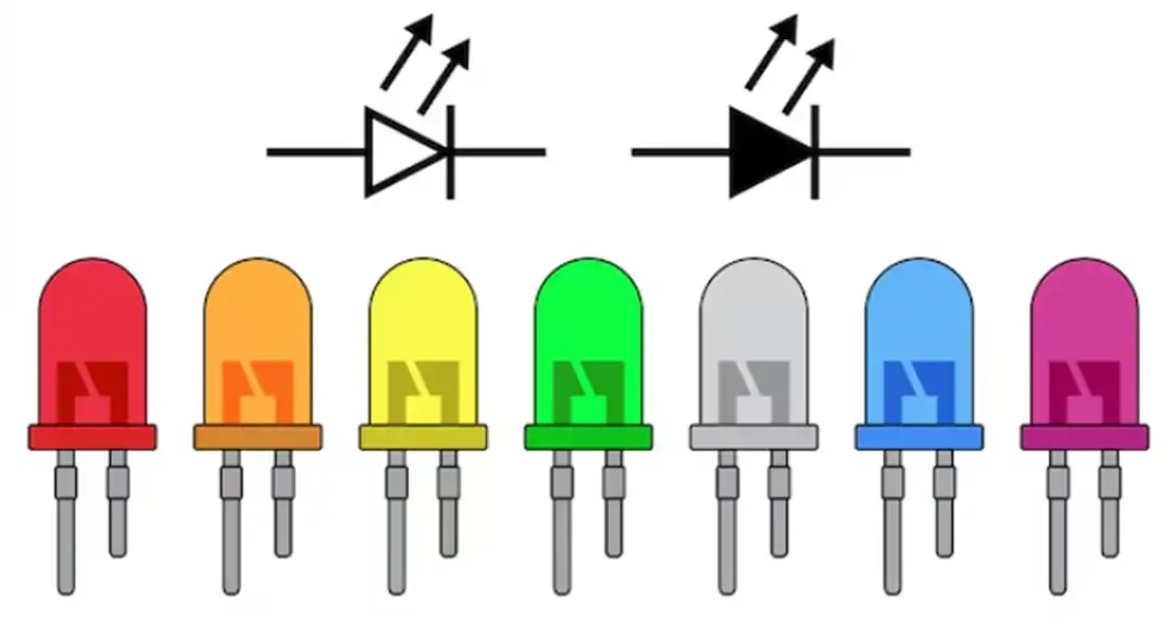
The three devices—LEDs, diodes, and photodiodes—use the same diode body, so the fastest way to differentiate between them is by observing the direction of the optical arrows on the symbols. The arrows indicate whether light travels away from or toward the device and do not indicate electron flow or conventional current through the diode body.
CAD libraries commonly provide ordinary diodes, LEDs, and photodiodes as separate symbols. The outward arrow direction remains the same no matter how the symbol is turned, and the cathode bar identifies K regardless of how the symbol is oriented.
How Does an LED Produce Light?
An LED is made by forming a p-n junction in a semiconductor to allow the release of energy as visible or IR light. When charge carriers cross the junction under forward bias, they recombine and release energy as photons. The semiconductor's bandgap determines the energy of the photons emitted, strongly influencing the resulting wavelength or color of the emitted light.
The arrows indicate emitted optical energy, while the body of the diode and the position of the cathode bar indicate the electrical polarity. The schematic does not give an exact measure of brightness, wavelength, viewing angle, efficiency, or spectral distribution. The exact values should be obtained from the manufacturer's specific datasheet.
Which Side Is the Anode and Cathode?
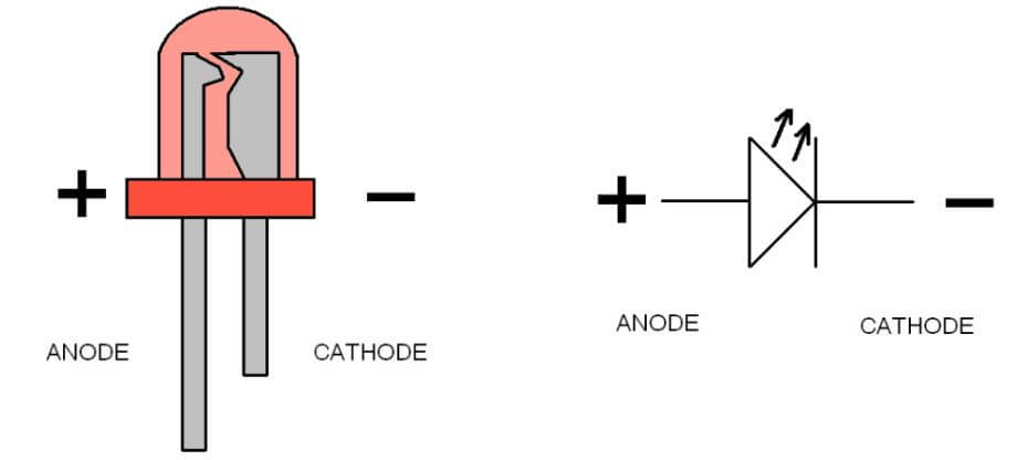
To find the terminals, first locate the cathode bar, which indicates that terminal K is connected to this bar, while terminal A is connected to the opposite side. When the LED is forward biased and used within the manufacturer's specifications, conventional current will flow from terminal A to terminal K. This rule applies regardless of which direction the LED symbol faces, whether left, right, down, or up.
Do not interpret the electrical polarity of the LED symbol as implying a certain power-rail connection. In some cases where the LED is used as an indicator, the cathode may connect to ground, whereas in other applications, such as high-side drivers, multiplexed displays, charlieplexed networks, and switching circuits, the cathode may connect to a driver output, another LED, or a node other than ground. The connections will be defined by the netlist; the cathode bar will identify the terminal.
The pin numbers are specific to both the library and the type of device. For example, KiCad's generic LED symbol typically designates K as pin 1 and A as pin 2. However, a vendor could designate different pin numbers and use a different library or package design. Verify the pin names and numbers in the symbol properties before assuming that K is pin 1.
What Happens If an LED Is Reversed?
When reversed, most LEDs will not illuminate because they are reverse biased. Many indicator-type LEDs have relatively low reverse-voltage tolerances. Therefore, if a reverse voltage exceeding the manufacturer's indicated limit is applied, it can cause leakage, degradation, or permanent damage to the junction. An antiparallel diode, a second LED, or another protection method may need to be incorporated into some alternating or bidirectional circuits, depending on the actual voltage and waveform.
Common LED Symbol Variants
In addition to the outward-arrow convention signifying light emission, there are many different package types and internal topology variations. Therefore, the schematic symbol must also include a separate representation for every independently controlled die, all shared terminals, and all integrated functions that affect connectivity.
An RGB package that uses six pins, such as the ams OSRAM KRTBLFLM71.32, contains a combination of red, green, and blue LED chips, also known as dies. The footprint and library symbol for such a device must show all six documented connections as specified in the datasheet.
How Do You Read an LED in a Basic Circuit?
A typical circuit for a basic DC-powered indicator usually has the LED and a current-limiting resistor connected in series. The current-limiting resistor may be located either on the anode side or the cathode side of the LED. When connected in a series circuit, both the LED and the current-limiting resistor carry the same current. To determine the value of the current-limiting resistor, you must know the power supply voltage, the forward voltage of the LED at the selected operating point, and the desired LED current.
Single LED: R = (Vₛ − Vꜰ) / Iꜰ
Series LEDs: R = (Vₛ − ΣVꜰ) / Iꜰ
For a supply voltage of 5 V, with a forward voltage of 2.0 V at the intended operating point and an intended forward current of 10 mA, the resulting resistance value would be 300 Ω. Selecting the standard 330 Ω value would provide close to 9 mA before accounting for component tolerances and temperature variations.
Do not assume Vꜰ or maximum current from the schematic symbol. Color, semiconductor material, temperature, production spread, and the conditions under which the LED operates influence Vꜰ and the maximum current rating. Always refer to the curves and ratings in the datasheet for the exact manufacturer part number. In a parallel-connected array of LEDs, provide separate current control for each branch because minor differences between Vꜰ values can lead to unequal current sharing.
Reading a Rotated or Mirrored LED Symbol
Rotation does not change terminal identity. Look for the cathode bar, confirm the anode (A) and cathode (K) designations and their pin numbers, and then trace the connected nets. Rules such as “the left side is the cathode” or “the top pin is positive” are invalid when the symbol is rotated.
Mirroring may visually swap left and right while also retaining or changing the CAD pin labels. The displayed pin names and numbers must ultimately determine the pin arrangement; it cannot be determined simply by looking at the symbol’s position on the screen. A mirrored package drawing can create an additional problem: the bottom view in a datasheet may appear reversed when compared with the top view of the PCB.
From Schematic Symbol to Physical LED
A correct symbol can still produce a reversed board if the numbered pad map, package view, or placement orientation is wrong.
Through-Hole Polarity Cues
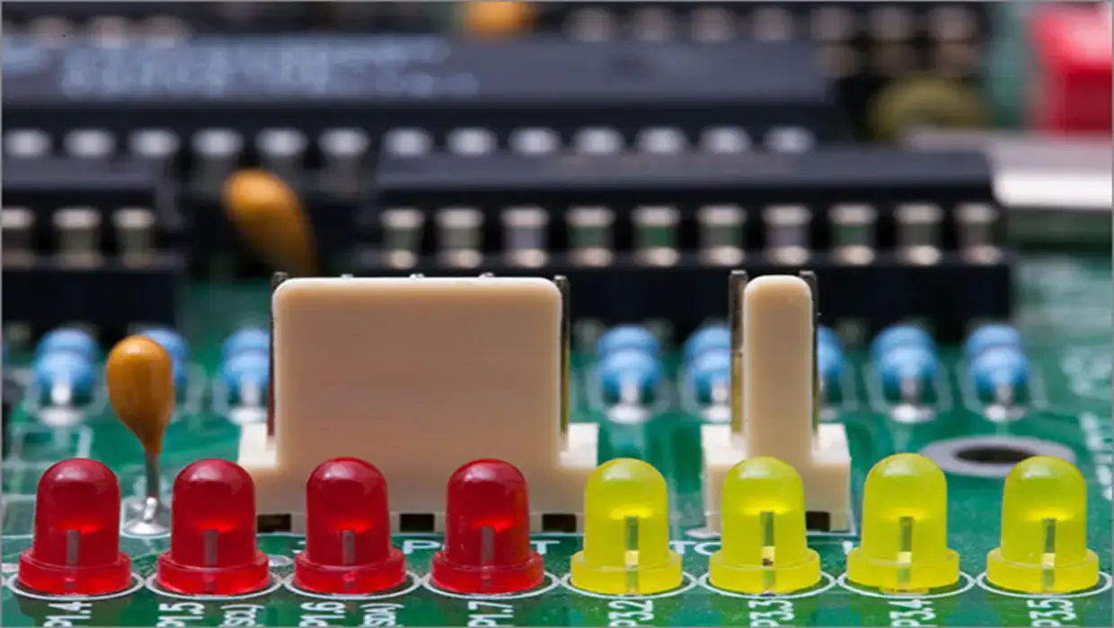
For many new through-hole LED devices, the longer lead is the anode, the shorter lead is the cathode, and a flat area on the lens body identifies the cathode side. While these are helpful secondary ways to confirm polarity, they should never replace consulting the datasheet. After the leads have been trimmed, formed, or inserted, lead length may no longer be a reliable indicator. Molded-body details also vary by package style. For example, square and rectangular lens bodies typically do not have flat edges. When determining the polarity of such components, the internal lead frame visible through the lens is the more reliable cue, as the larger, flag-shaped lead frame usually indicates the cathode.
SMD Polarity Cues
SMD LEDs may use various markings, such as a line, dot, notch, chamfer, underside pattern, colored mark, or package corner, to indicate their orientation. However, no single mark is universal among all manufacturers and package types. For example, the Vishay VLMW1320-GS08 0603 ChipLED marks the cathode on the physical package outline as a molded feature of the package, not a printed dot. The ams OSRAM LS T676, a PLCC-2 TOPLED with an integrated reflector, instead shows the anode and cathode through different copper-pad shapes in the recommended PCB footprint. Thus, the orientation indicator is in the PCB land pattern rather than on the physical component. When you copy a footprint from one LED package to another or read the footprint from the wrong reference, the anode and cathode may be swapped without any visible indication. Therefore, you must read the exact package drawing and its stated top-view or bottom-view orientation before transferring the LED mark to the footprint or assembly drawing.
How Do You Verify LED Polarity Before PCB Release?
- Identify and record the LED terminal designations, A and K, with their respective symbol pin numbers. The cathode bar and terminal labels help identify polarity; do not rely on orientation, such as left or right, or a memorized library convention.
- Compare the pin numbers from the schematic symbol with the numbers on the footprint pads. Confirm that each symbol pin number corresponds to the pad with the same number to avoid using a footprint that appears correct but has electrically reversed pads.
- Confirm that you have the complete manufacturer datasheet for the LED. Verify the manufacturer part number, package suffix, pinout, polarity mark, and stated view direction. For bi-color or RGB LED components, verify every die and common terminal, not just the package outline.
- Compare the verified footprint with the silkscreen, assembly drawing, BOM, approved alternate parts, and placement data. Confirm the board side and centroid rotation to avoid mistakenly mounting a correct footprint backward during assembly.
The review evidence should show matching identifiers, not similar shapes: A and K terminal designations, symbol pin numbers, footprint pad numbers, manufacturer-specified pin designations, and documented package markings. If an approved alternate source defined by the BOM is used, repeat the verification of the LED package markings and pinout instead of assuming that an electrically equivalent LED uses the same orientation cue.
Common LED Symbol and PCB Mapping Errors
Interpreting the outward arrows pointing away from an LED as representing the direction of electrical current flow rather than determining current direction from the polarity of the diode.
Determining polarity, K and A, based on the location of an LED symbol on a computer screen. The symbol’s location does not reliably establish the left/right or top/bottom position if the LED symbol has been rotated or mirrored.
Assuming that K and A always refer to pin number 1 and pin number 2, respectively, and that this is true for every manufacturer’s symbol. This convention may be true for one library item; however, there are exceptions for other libraries, vendor symbols, and multi-die LED devices.
Using visual similarities in shape to match a symbol to a footprint rather than matching the symbol pin numbers to the footprint pad numbers. A visually similar footprint may still have electrically reversed terminals.
Reading a bottom view of a package drawing as a top view. This produces a mirrored pad map even if the datasheet pin numbers have been copied correctly.
Incorrectly using the same polarity marker for every SMD LED. A dot, notch, line, or chamfer has meaning only within the exact manufacturer package drawing.
Using the correct footprint but selecting the wrong package suffix or approved alternate. Similar product names may have different internal pin configurations and orientation marks.
Making the assembly drawing or placement rotation inconsistent with the verified footprint. The PCB design may be electrically correct in CAD but still be populated backward.
Final Check
Every LED anode and cathode connection should be traced by an independent reviewer from the schematic symbol through each numbered footprint pad to the exact package drawing and placement orientation. If any connection is based on visual convention, a universal SMD polarity indicator, or an assumed pin number, the polarity check is incomplete.
References & Sources
- 1. IEC 60617 — Graphical Symbols for Diagrams
- 2. KiCad Device Symbol Library — Device.kicad_sym
- 3. KiCad Schematic Editor Documentation
- 4. Altium Designer — Validating Your Design Project
- 5. Vishay VLMW1320-GS08 Highbright 0603 ChipLED
- 6. ams OSRAM LS T676 Datasheet
- 7. ams OSRAM KRTBLFLM71.32 Datasheet
- 8. LED – Light Emitting Diode | Basics, Working, Structures, and Applications — Engineering Funda