Upload BOM & Gerber

FPGA is short for field programmable gate array. Programming an FPGA creates a digital circuit from the programmable logic resources and routing capabilities. When programming microcontrollers and microprocessors, they load instructions that run on an existing processor architecture; therefore, all three of these devices change the behavior of a product, but do not alter the same object.
An MCU integrates a processor with memory and control peripherals. An MPU supports broader software capability, interfaces, and external memory, often with a full operating system. The FPGA can build unique connections, paths, and interfaces for custom hardware. Once you have selected the execution model, you will use that information when designing the PCB.
Contents
show
What Does FPGA Mean, and What Is Inside One?
The FPGA configuration memory provides the means for controlling the logic elements and programmable interconnects and for defining a digital hardware architecture on an FPGA after it has been manufactured. The term “field” implies that you can reconfigure or rebuild an FPGA outside of the semiconductor factory.
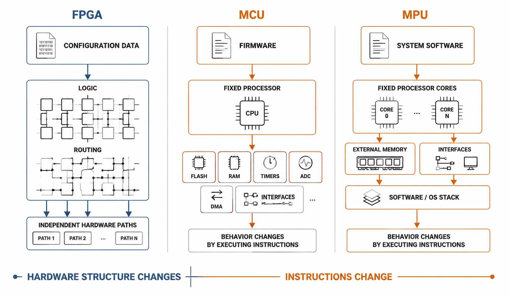
An FPGA has multiple logic resources, typically comprising lookup tables, registers, programmable interconnects, I/O blocks, clock resources, block RAM, digital signal processing blocks, and many other components. Some families of FPGAs include hard processors, high-speed transceivers, and other dedicated features. Each of these features is typical for that family and not universal for all FPGAs. Each FPGA has its own part number and family documentation indicating what features and resources it provides.
A bitstream consists of configuration information and provides the means to define both the functionality and connections of an FPGA. It is not simply a CPU program with an alternative name. After loading the configuration data into an FPGA, the resulting connections can function independently as state machines, counters, interfaces, memory units, and pipelines.
FPGA configuration storage exists as memory separate from application data memory and can vary in how it starts up and retains data depending on the device technology. The configuration information for Lattice iCE40 devices is an example of a volatile SRAM configuration, while other iCE40 devices have nonvolatile memory built in. For this reason, the statement “all FPGAs forget their configuration after removal of power” is not always accurate.
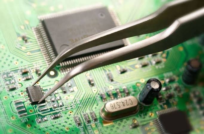
The packaging illustrations do not identify categories. A similar package may include an FPGA, MCU or MPU, memory, or other devices, but the part number and controlled documentation identify the exact device; do not use a generic board photograph to identify the IC part number.
FPGA vs MCU vs MPU: The Architecture at a Glance
At a glance, FPGA, MCU, and MPU are all capable of processing inputs and controlling outputs; however, the difference is the object changed, integration boundary, and development artifacts for each of these three devices.
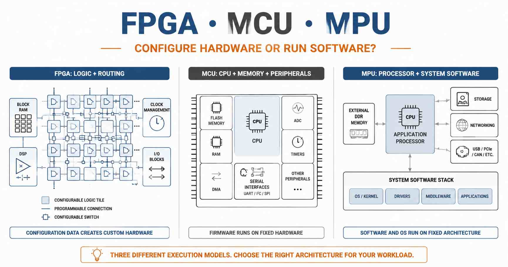
The STM32G4 series of MCUs is an example of how an MCU can be more than just a CPU that executes one task at a time. In addition to the Cortex-M4 core, they contain Flash memory, RAM, timers, converters, communication interfaces, and mathematical accelerators. Additionally, Microchip provides information about their core-independent peripherals, which can operate with limited CPU intervention on supported PIC and AVR families.
An MPU is more than a fast MCU. When the software system becomes a primary requirement of the design, an MPU can become the selected platform. Microchip’s 32-bit MPUs showcase Linux-capable systems, external memory connectivity, and module options, although individual products vary. The processor is one part of the end product derived from an MPU, but there are differences in boundaries between motherboards and system boards.
ASICs and CPLDs are boundary cases; they do not address the same problems identified above. CPLDs typically target smaller programmable logic functions where modest logic density and predictable control matter. ASICs are fixed at manufacture time and offer benefits regarding unit production costs, power, or area for large volumes. However, they require non-recurring engineering for each use and remove field reconfiguration after manufacturing.
What Is the Difference Between Developing an FPGA and Developing Firmware?
FPGA development defines, verifies, and implements the design onto FPGA resource locations. Firmware development involves compiling and linking instructions for an existing processor. MCU and MPU software is commonly written in C or C++, while RTL for most FPGAs uses Verilog, SystemVerilog, and VHDL. The fundamental difference is the execution model. HDL describes hardware structures and concurrency, while the microprocessor executes instructions on a fixed architecture. Both require requirements, source control, verification, testing of the end result, and full target validation of the project. Each has different implementation risks.
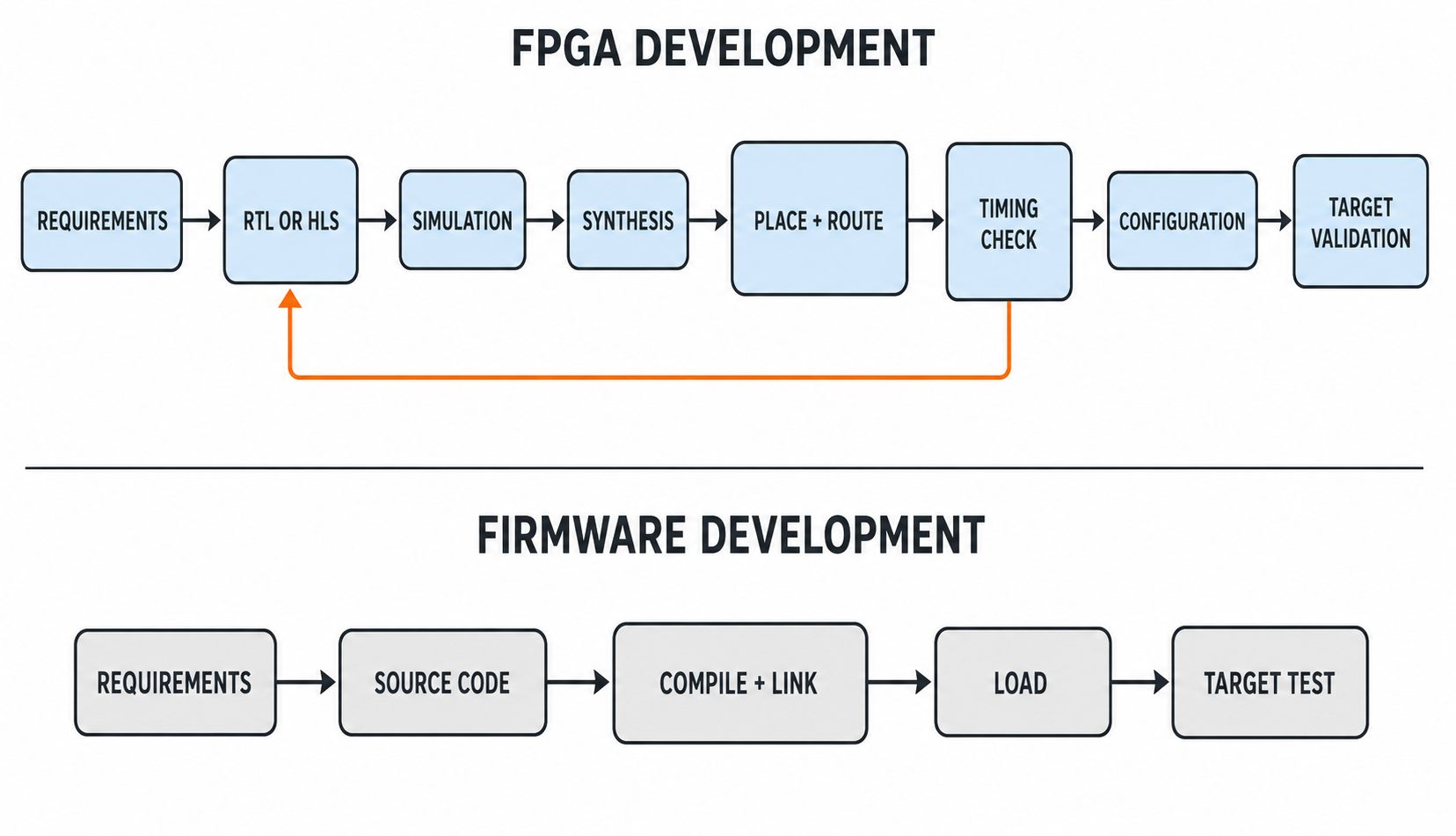
An FPGA development flow consists of the following processes, in order:
- Define interfaces, clocks, throughput, latency, and reset behavior.
- Define hardware using RTL (Verilog, VHDL, SystemVerilog, etc.) or other suitable design representations.
- Simulate and verify the expected behavior of hardware using testbenches.
- Synthesize the hardware as a logical netlist.
- Place and route that logic within the target device.
- Check timing closure, clock-domain crossings, resources, and implementation reports.
- Generate configuration data and validate the configuration data on the target hardware.
AMD’s Vivado documentation details FPGA synthesis, implementation, timing inspection, and bitstream generation, while the Vivado Implementation Reference document subdivides the implementation phase into the stages of optimization, placement, routing, and device-image generation. While the implementation process uses terms that vary from company to company, what distinguishes it from a firmware compile is fundamentally different.
One cannot assume that clean HDL or a nominal clock target is reflective of timing closure. Factors such as routing delay, where resources are placed, fanout, clock-domain crossings, and various constraints shape whether or not the circuitry will perform according to specification. An FPGA development group primarily concentrates on hardware verification and implementation reports, while a firmware team focuses more heavily on instruction behavior, interrupt timing, peripheral state, memory, drivers, and operating-system integration.
An FPGA development project requires resources that can validate various aspects of the project leading to the final product in addition to having programming abilities.
Performance, Power, and Cost Depend on the Workload
There is no single category of devices that is always the fastest, the lowest power, or the least expensive. Valid comparisons must specify the workload, the devices being compared, the interfaces, the measurement point, and the engineering constraints. Simply comparing clock frequency cannot determine which architecture will provide the best performance.
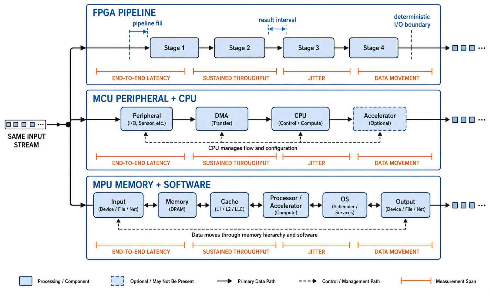
For example, with a fixed transform applied to a continuous sample stream of data, the FPGA could build several pipeline stages and accept a new sample each clock cycle after the pipeline becomes fully filled, if timing and resources permit. Using this type of implementation, the FPGA could achieve very high sustained throughput rates, with predictable I/O timing. The first result still experiences pipeline latency, so throughput and latency remain different measurements.
Using the same example, a CPU may perform the transform through its instruction set by making use of cache memory, memory transfers, SIMD instructions, or a dedicated accelerator. This can win when the data rate is moderate, the libraries are mature, the branches are irregular, or there is frequent change in the underlying algorithm. Similarly, the peripherals and DMA within MCUs enable them to move data while the CPU performs control tasks and processing.
In Lattice’s case, the iCE40 LP/HX Datasheet specifies standby current as low as 21 µA for the iCE40LP family; however, there is no indication of what the same silicon chip will do when running a functional active design at full clock rates or how it would compare to larger and higher-density FPGA families designed to maximize logic capacity instead of low power mode capabilities. Similar to power usage, cost claims will only become comparable once you consider the board area used, the external memory devices used to support the design, the cost to license the design tools used to develop the design, and the time taken to verify the produced designs; a device’s pricing can lose its competitive advantage when it becomes significantly more expensive due to additional external hardware or engineering work.
It is generally simpler to deliver and support control products with modest I/O complexity, frequently changing features, complex branches, and existing software libraries on an MCU than it would be on an FPGA. An FPGA could definitely implement the logic required. Configurability does not justify the burden of verifying each configuration.
Which Architecture Fits Your Workload?
Deciding which architecture is appropriate depends on measurable execution and system constraints. When determining which architecture to use, begin by examining I/O and software because they typically limit the number of options considered before clock speed starts to become a comparison factor.
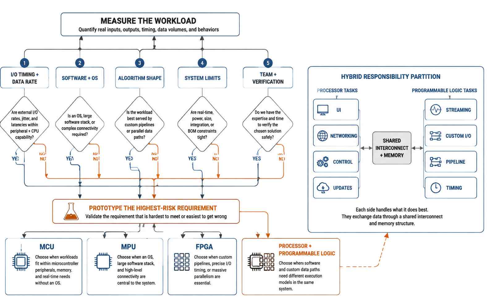
- Quantify Input/Output. Determine the number of channels, protocols used, line rates, sample rates, latencies, jitter, and how synchronization will occur.
- Define Software. Specify whether the software will be bare metal or whether an RTOS, Linux (or other) software drivers, networking, graphics, storage, security updates, etc. will be required.
- Identify Algorithms. Separate fixed streaming paths and independent channels from irregular control flow patterns.
- Establish System Limits. Define the power state, thermal path, startup, total unit cost, required board area, and expected production volume.
- Check Ownership. Review whether you own (or have access to) RTL files, firmware, Linux and verification skills, timing analysis, test automation, and lifecycle skills.
- Prototype the highest risk item. Prove the requirement most likely to invalidate your selected category.
Four Architecture Examples
- Controller for motor or sensors: Use an MCU, which includes integrated ADCs, timers, PWM, DMA, and communication peripherals. All interrupt loads and timing must be verified for peripherals with requirements for memory headroom and power states before starting with programmable logic.
- HMI based on a Linux OS or as a network gateway: If the product requires Linux OS, large memory, networking stacks, graphics, storage, or complex applications, starting with an MPU is appropriate. The emphasis will shift to boot time, external memory bandwidth, thermal behavior, and any hard real-time requirements.
- SDR (software-defined radio), high-speed camera, or custom digital interface: The appropriate starting point is an FPGA. For several processes running concurrently with deterministic timing or unusual protocol widths, the throughput, end-to-end latency, buffer behavior, resource usage, and timing closure on the specific target device must all be measured.
- A combination of rich software and a deterministic data path: In this case, a CPU and an FPGA would be used. When complex software or Linux OS will be used along with a fixed-latency interface or pipeline, define which side of the interface will own (or control) the various buffer types, interrupts, clocks, resets, and memory bandwidth before the cross-domain path is verified under worst-case load.
AMD has documented Zynq 7000 as a combination of a processing system with integrated programmable logic in a single die.
The Embedded Design tutorial shows that the Processing System can run independently or connect to IP in programmable logic. This supports a “clean partition” between software on the Processing System, networking interfaces, and user interfaces, while selecting only specific interfaces or pipeline connections within the hardware.
There is also another option of implementing a soft processor into a PLD and a hard processor manufactured beside the programmable logic fabric. These options are not available uniformly across the different FPGA families. The selection of the target device should be made based on the technical characteristics of the FPGA family rather than making an assumption that the term “FPGA” will automatically provide the desired processor configuration.
How Does Architecture Choice Affect PCB Design?
Once the desired architecture has been selected, the architecture must be translated to the following parameters of the PCB’s inputs: power, memory, configuration, and clocks; as well as startup, I/O standards, connectors, debug access/test, and thermal limits. An MCU is able to maintain a compact BOM because Flash, RAM, timers, and converters are integrated peripherals; however, analog references, decoupling, clocking, and debug access still need explicit verification.
An MPU-based board generally uses external memory, boot storage, PMIC or sequencing, higher-speed interconnects, and a greater thermal and software boot dependency. An FPGA board may require multiple rails, I/O-bank voltage constraints (as with Altera’s Cyclone family), configuration circuits, clock-quality specifications, dense BGA breakout, and JTAG or other types of debug access.
In the case of fast memory or, in some cases, high-speed interconnects, review the high-speed PCB design constraints specified by the device chosen, including “Signal Integrity” and “Power Integrity,” instead of relying on the device category to provide these characteristics.
Frequently Asked Questions
Q1. Is an Arduino or Raspberry Pi an FPGA?
By definition, neither. Arduino and Raspberry Pi are platforms or brand names, while FPGA, MCU, and MPU describe semiconductor architectures. Many Arduino boards use an MCU, while many Raspberry Pi boards use an application processor or SoC. Some specialized boards use programmable logic. Therefore, always verify the exact board revision and chip when classifying them by brand name.
Q2. Does every FPGA need external configuration memory?
No. Configuration technology and boot options vary throughout different FPGA families. Some SRAM-based devices load their configuration from external memory or another controller, while some families of devices provide nonvolatile configuration options built into the FPGA. An example of both volatile SRAM and nonvolatile configuration technology can be found in Lattice’s iCE40 documentation. The device datasheet governs startup and retention characteristics.
Q3. Is an FPGA digital or analog, and does AI require one?
No. FPGAs are primarily configurable digital logic fabrics, although some specific manufacturers have produced digital logic fabric FPGAs designed to augment digital logic functionality through the addition of converters or analog-related modular blocks. Therefore, determining whether an FPGA is suitable to accelerate or run AI workloads should be based on comparisons of the model’s latency, throughput, power, memory movement, software support, needs for updates, and development cost.
Conclusion
For integrated control systems, use the MCU if the peripherals and timing capability are sufficient; use the MPU if a rich software system and larger memory dependency dominate; use the FPGA when hardware verification justifies custom parallel data paths and deterministic I/O; and use a processor plus programmable logic architecture when both are required. Transfer power, memory, clock, startup, I/O, thermal, and testing characteristics into PCB implementation.
References & Sources
- FPGA Architecture, UG1291 – AMD
- Step 2: Synthesizing, Implementing, and Generating the Bitstream, UG986 – AMD
- Implementation Sub-Processes, UG904 2026.1 – AMD
- Zynq 7000 Processing System IP – AMD
- Using the Zynq SoC Processing System, UG1165 – AMD
- STM32G4 Series – STMicroelectronics
- Core Independent and Analog Peripherals – Microchip Technology
- 32-bit MPUs and Hybrid MCUs – Microchip Technology
- iCE40 Programming and Configuration – Lattice Semiconductor
- Choosing Between Microprocessors, Microcontrollers, and FPGAs: A Comprehensive Guide ! – TechSimplified TV