Upload BOM & Gerber

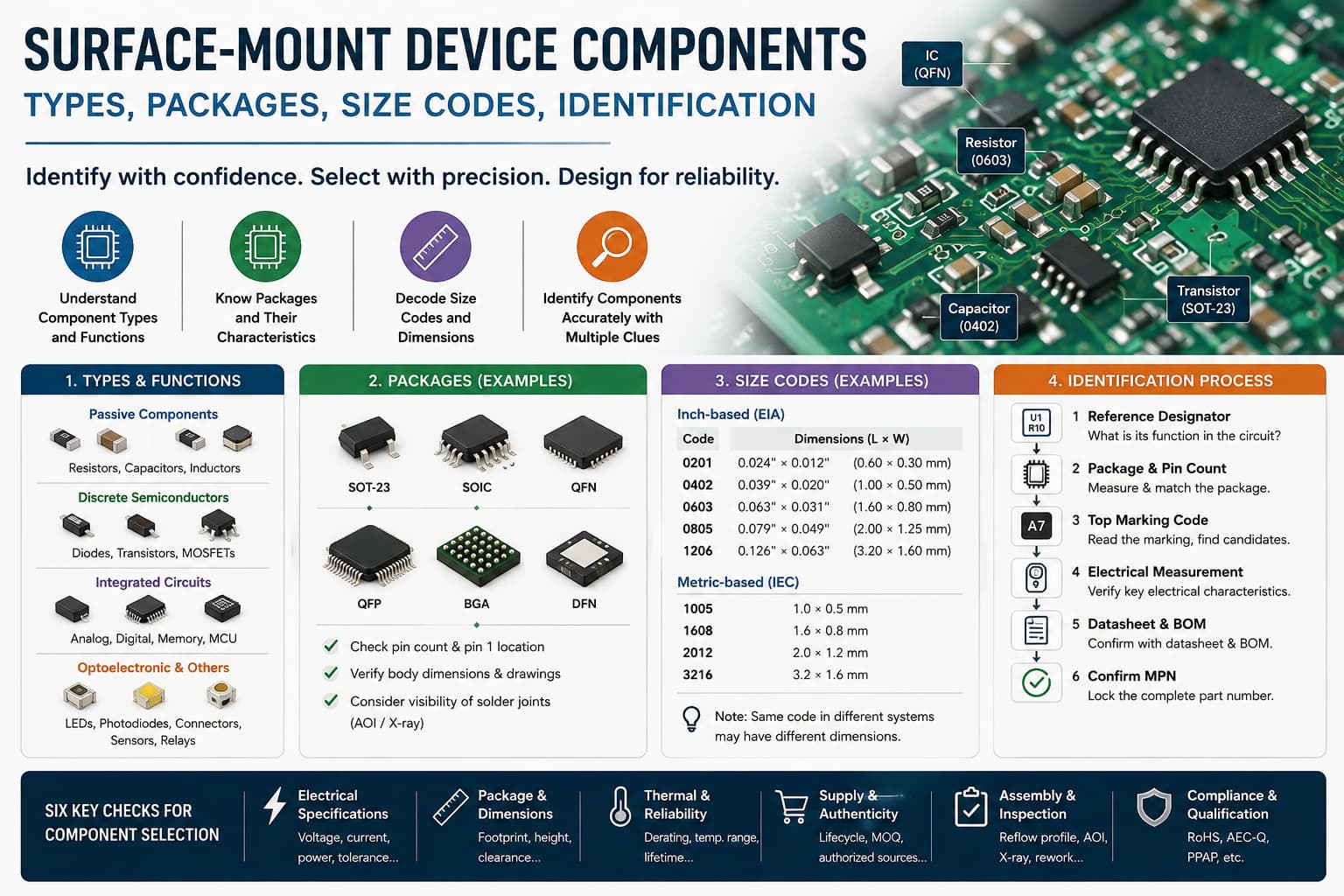
A component's appearance—either a tiny black rectangular body or a beige rectangle—can narrow its overall size and the family or package type it belongs to, but does not define how the component functions electrically or the exact orderable part number.
Reliable classification of SMD components requires consideration of three questions: what the component does; how the terminals connect to the printed circuit board (PCB) at the time of assembly; and what manufacturer part number best fits the available evidence.
The complete definition of an SMD component should include the electrical specifications of the component, the complete manufacturer part number, a drawing of the physical package, the footprint of the package, the orientation of the component when placed on the PCB, and approved supplier information.
Descriptions of SMD components as "0603 capacitor" or "SOT-23 transistor" do not answer questions regarding the actual value, rating, pinout, qualification, or ordering-suffix decisions.
Contents
show
What Are Surface-Mount Device Components?
Surface-mount device (SMD) components are electronic parts designed for attachment to lands on a PCB surface, most commonly through soldered terminations. SMD refers to the actual physical device, while surface-mount technology (SMT) is the term given to the manufacturing process used to attach and join these devices to PCBs.
An SMD could be any type of electronic functional component, including resistors, diodes, transistors, integrated circuits, LEDs, sensors, switches, connectors, etc. The package of an SMD represents the mechanical interface of the SMD to the PCB, through which electrical connections are made. The electrical category and package family of an SMD correspond to different aspects of the SMD. The first corresponds to the behaviour of the SMD and the important electrical ratings for that SMD. The second is related to the dimensions, terminal geometry, terminal pitch, heat flow, footprint, and access to the SMD for inspection and testing purposes.
For the basic SMD definition, SMD-versus-SMT terminology, through-hole comparison, termination styles, and the introductory identification sequence, see What Is an SMD? Surface-Mount Devices Explained.
Surface-Mount Component Types by Electrical Function
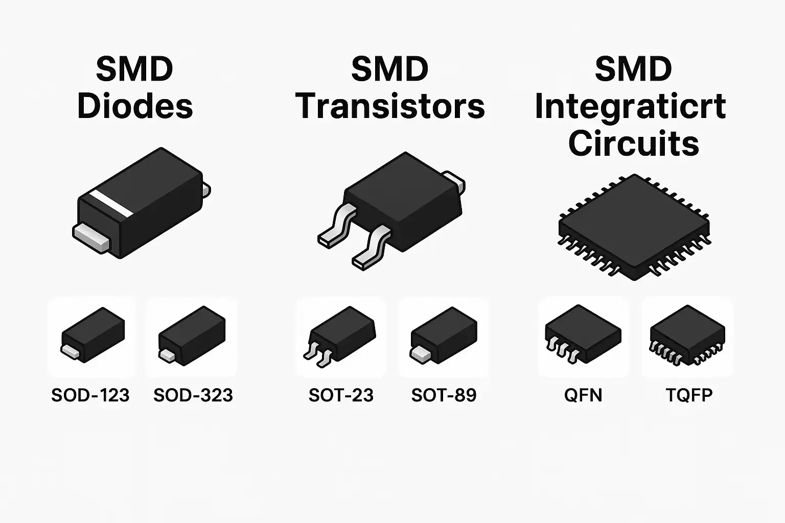
A practical first classification uses electrical function because it identifies the specifications that control circuit behavior. The package can narrow the candidate, but replacement and design decisions begin with the component's role and operating requirements.
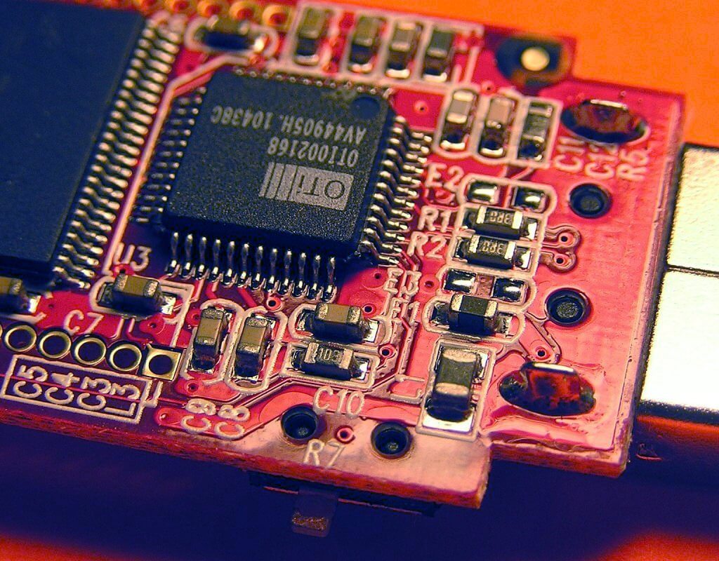
Various reference-designator conventions exist within companies and schematic libraries. The conventions indicate the intended circuit category rather than the manufacturer's part number. A repaired board may have substitute parts that are valid replacements for the original part number listed on the BOM.
When considering passive components, you have to take into account that they may have similar outlines but behave differently. For example, chip resistors, multilayer ceramic capacitors, inductors, and ferrite beads may all use a rectangular two-terminal package body, and colour is not a reliable means of identification. The reference designator and circuit position will indicate a potential category, but to determine compatibility, value, material system, tolerance, voltage or power rating, frequency behaviour, and manufacturer documentation will be required.
Discrete semiconductors introduce additional constraints with respect to polarity and terminal mapping. Integrated circuits are even more constrained than discrete components because unrelated components may have similar packages and incompatible pinouts. The complete ordering code is important, as each suffix may indicate package, packing, temperature grade, automotive qualification, lead finish, or some other purchasable variation.
Optoelectronic, sensor, and electromechanical components couple physical direction with electrical behaviour. For example, the emitting axis of an LED, the window of a sensor, the port of a microphone, or the mating direction of a connector can result in an electrically compatible component being unusable in the physical layout.
How Do Package Families Describe Physical Connections?
Package families provide a general description of where terminals are located and how they attach to the PCB lands, but they do not give a specific name or description for a component. Therefore, one electrical component may be available in many different packages, while a single package family might include thousands of unrelated components.
As documented by Nexperia and onsemi, SOT-23 drawings show a nominal 2.9 × 1.3 × 1.0 mm three-terminal body, 0.95 mm adjacent-pin spacing, and 1.90 mm spacing between the two outer pin positions. These are different dimensions and should not be substituted in a footprint check.
The exact product and case drawing control terminal mapping, marking, and function. Terminal identification may also be indicated by surface markings such as dots, stripes, notches, bevels, and molded features; however, the identification should be verified against the manufacturer's drawings. For example, while a stripe on a diode may indicate cathode orientation and a dot on an IC may indicate pin 1, these markings do not provide a common reference across all manufacturers and product families.
Gull-wing lead packages generally allow most joints to be visually inspected during assembly via a camera; however, joint access in QFN, LGA, BGA, and WLCSP packages is blocked by the body of the package. Therefore, these package families may require X-ray inspection or evidence of process control before acceptance rather than visual inspection alone. Consequently, inspection access is a major factor in package selection and should be considered before PCB release.
What Do SMD Size Codes Actually Mean?
SMD size codes provide a short package identification or label rather than complete dimensions or electrical specifications for a given component. Inch-based and metric systems are common for most passive chip components. Both systems may use four-digit identifiers; therefore, the BOM and footprint library should identify the measurement system and retain the manufacturer's original drawing for reference.
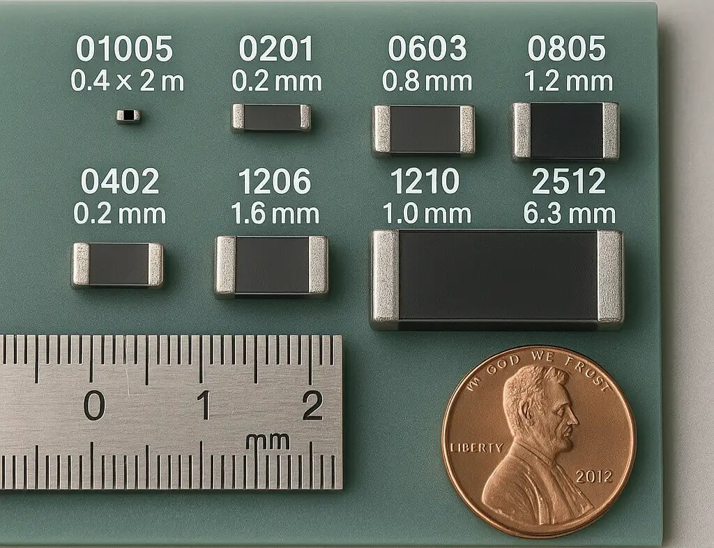
The two conventions can use the same four digits for different sizes. The code “0603” indicates a size of 1.6 × 0.8 mm under the imperial system, but the same code indicates a size of 0.6 × 0.3 mm (imperial 0201) under the metric system. If a BOM or silkscreen note does not include the convention label, it could send the wrong size directly into placement, with no error indicated until the first article is built.
A size code by itself provides no information about capacitance, resistance, voltage, power level, dielectric, temperature coefficient, pulse capability, current rating, or environmental grade. Even if two components have the same size, they can require different land patterns or assembly controls due to differences in their terminations, component thicknesses, and manufacturer recommendations for assembly process control.
Family names for integrated circuits and discrete semiconductors, such as QFN, TSSOP, SOT-23, PLCC, and BGA, describe package families; however, they do not represent the full set of dimensions needed to make an accurate comparison. Body dimensions, pin or ball pitch, terminal or ball count, exposed-pad dimensions, height, and the current drawing of the particular package must also be included. In cases where there is a conflict between library nicknames and approved documentation provided by a manufacturer, the manufacturer's approved drawing takes precedence in making footprint decisions.
Just because the smallest package size is available does not mean that it is the best option. Factors including voltage and power derating, heat dissipation, placement capability, inspection access, rework method, handling method, and supply continuity might preclude using the smaller package style even if it fits into the available area on the board.
How Can You Identify an Unknown SMD Component?
When identifying unknown SMD components, it is critical to combine independent evidence and document the level of confidence in the identification. The evidence for identifying an unknown component will typically include body shape or top marking, and more than one piece of evidence may lead to an identification. To verify an identification, you will need compatible dimensions, terminal arrangement, orientation, circuit function, ratings, records, and manufacturer documentation. If you have conflicting or incomplete information in these areas, you should flag the component as “unresolved” instead of assigning a guessed part number.
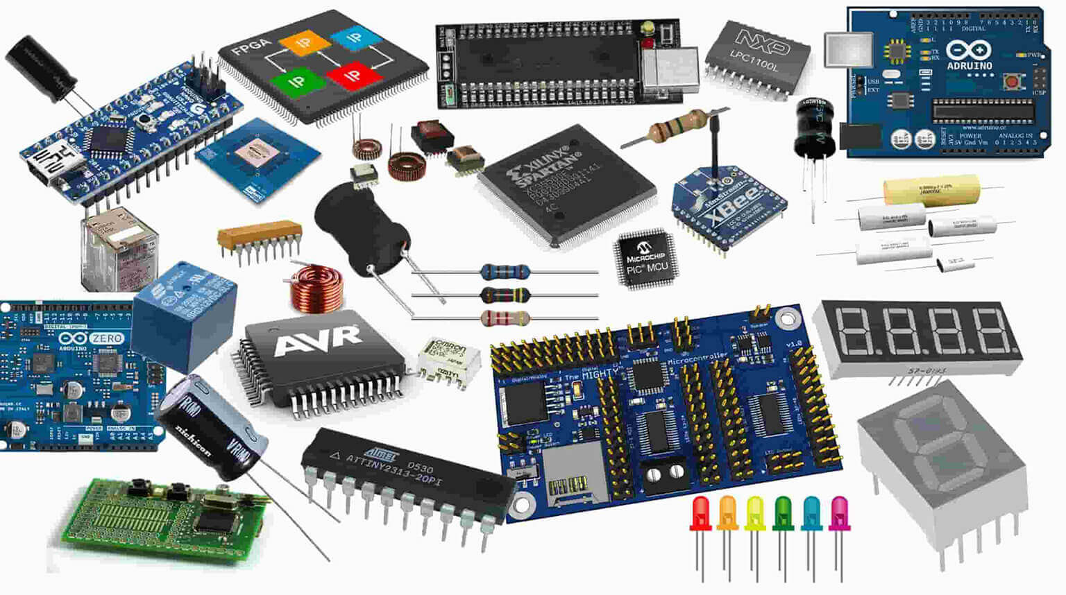
When using a manufacturer marking tool, one searches a manufacturer’s documented products. While the TI manufacturer marking tool will help narrow down TI devices, it is not able to search the catalogs of other vendors. Many shorter markings combine a device code with lot, date, grade, or assembly information, while some very small parts do not have readable markings.
While electrical measurements can eliminate or confirm candidates for the device, electrical measurements taken in a circuit can be affected by parallel components, protection networks, bias paths, contamination, or damaged components. Resistance, continuity, diode, or capacitance readings should be taken on a de-energized, discharged circuit and interpreted against the circuit schematic. Lifting a terminal in a repair investigation may provide useful information, but it changes the configuration of the board and should not be used as the first step of the investigation.
A compatible replacement can be verified without proving the original installed MPN, provided its package, terminal mapping, ratings, circuit function, and replacement requirements are documented.
Choosing a Component and Package for Assembly
The choice of production-ready parts will involve more than simply obtaining the same nominal values and identifying the smallest applicable package. Six selection checks must be performed to connect the circuit requirement with an orderable component for which the physical construction, supply availability, and assembly method have been determined.
IPC lists IPC-7351 as no longer maintained and published IPC-7352 in 2023 as the Generic Guideline for Land Pattern Design. The generic guideline supports a consistent design method, while the selected component's current manufacturer drawing remains necessary for package-specific dimensions, terminal geometry, and recommendations.
The packing and presentation of a component must also be included in the definition of the component. The same body family may have various methods of presentation, such as different reel sizes, pocket orientations, tape widths, trays, or tubes. The selected component supplier should provide the appropriate packaging specification, which controls feeder presentation. The package also determines stencil planning, reflow limitations, inspection access, ESD or moisture handling, and the controlled rework tools used with the selected component.
Where Are Surface-Mount Device Components Used?
Compact Consumer and Wearable Electronics
Small-form-factor products utilize small passive devices, sensors, microphones, power-management integrated circuits, and dense packages that are confined by limited board area and height. Along with package size, it is also essential to consider additional factors affecting selection, such as battery and antenna clearance, acoustic or optical access, standby current, thermal management, double-sided placement, repair access, and supply continuity.
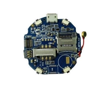
A microphone or sensor port placed a fraction of a millimeter from its stated position can be acoustically blocked once the enclosure seal closes over it. Board-level electrical or functional testing before enclosure assembly may not detect this condition.
Automotive and Industrial Controls
In general, control boards contain logic, sensing, protection, power conversion, communication, and mechanically exposed interfaces. When selecting components for these applications, the component selection process should include operating-temperature grade, voltage and transient margins, derating values, vibration sensitivity, coating compatibility, component lifecycle, approved alternatives, and traceability requirements.
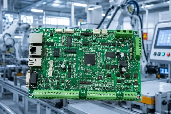
Two MOSFETs in the same TO-252 package can differ in automotive qualification status and operating-temperature rating. A same-footprint substitution may therefore fail the required qualification or thermal-cycling criteria even if first-article assembly is acceptable.
RF and Communication Circuits
In addition to matching nominal RF components on a PCB, it is essential to have package-aware electrical models of the RF components. The geometry of the package terminals, ground connections, package parasitic capacitance and inductance, frequency-dependent losses, S-parameters, and the transition from the RF package into the PCB must all be taken into consideration because they are significantly affected by the PCB implementation, layout, assembly, and measurement conditions. A smaller package may reduce one parasitic while creating tighter layout, assembly, and measurement constraints. Final behavior depends on the specific part and PCB implementation together.
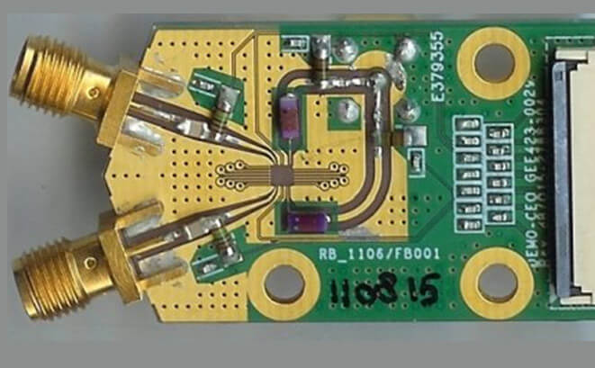
If a designer replaces an RF switch with a different vendor's pin-compatible part, it is possible for both the schematic and footprint of the RF switch to remain compatible, yet the shift in insertion loss may be enough for the RF switch to fail to meet the receiver's sensitivity requirements. The packages of the two switches matched, but the die and lead-frame parasitics differed significantly.
LED and Power Electronics
The important factors that LEDs and power-electronics devices, including drivers, MOSFETs, rectifiers, and regulators, have in common are polarity, current, dissipation, optical direction, and thermal paths. The use of an exposed pad is an effective way of providing ground, heat transfer, or both to the device. Evaluation of a device's copper area, thermal vias, board-to-housing contacts, void distribution, and operating-temperature conditions is only effective when using the exact package, as a generic SMD or power-package label does not specify any of the above criteria.
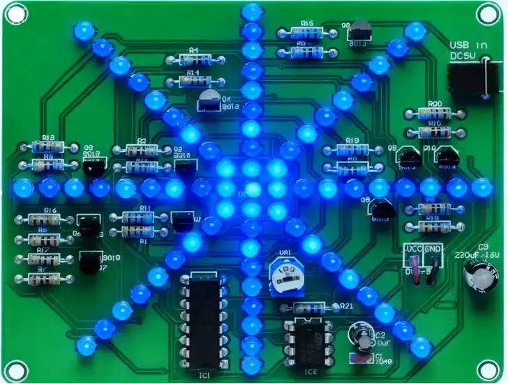
Two power MOSFETs in the same exposed-pad package may have different junction-to-case thermal resistance ratings. Therefore, a board design based on one device's copper-area requirements may run significantly hotter when another same-footprint device is substituted.
Medical and Measurement Equipment
Measurement and medical electronics tend to be more tightly controlled in terms of tolerance, drift, noise, leakage, temperature coefficient, cleanliness, traceable identity, and substitution control. Environmental rating and long-term stability are two significant areas that may vary materially between two devices with identical functions and footprints. Documentation of the approved MPN and its specified conditions must remain connected to the circuit requirement and all inspection records.
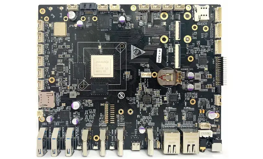
A precision resistor that is swapped with another resistor that has the same value and footprint but a wider temperature coefficient may pass an initial calibration test before it begins to drift when the enclosure temperature increases during continuous operation.
References & Sources
- SOT23 package information — Nexperia
- Package Drawing 318-08: SOT-23 (TO-236) — onsemi
- Mounting Methods for Chip Multilayer Ceramic Capacitors — Murata
- Device Marking Conventions — Texas Instruments
- Packaging Part Marking Lookup — Texas Instruments
- IPC Document Revision Table — IPC
- IPC-7352 Table of Contents — IPC
- Packaging: SMD Chip and MELF Resistors — Vishay
- How to Measure Resistance with a Digital Multimeter — Fluke