Upload BOM & Gerber

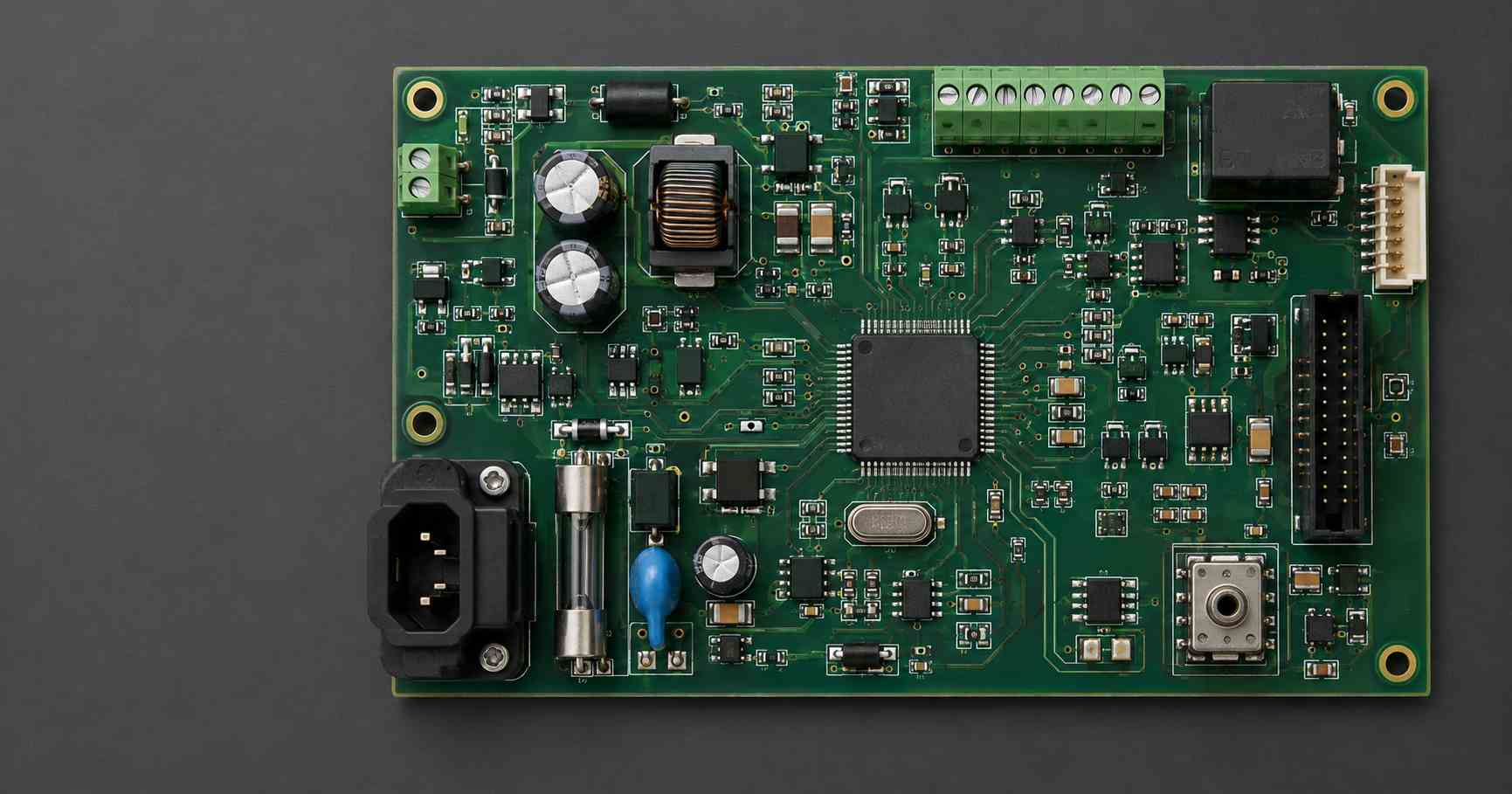
The populated circuit board can help determine the types of components it contains and the purpose of those components. But, by simply viewing the populated board, an individual will not be given the exact identity of a component. First, the visible object should be identified to determine the possible candidates for the component. Then, the populated board must be compared to the correct revision of the design file for that component, and finally, the manufacturer's datasheet for the component must be checked.
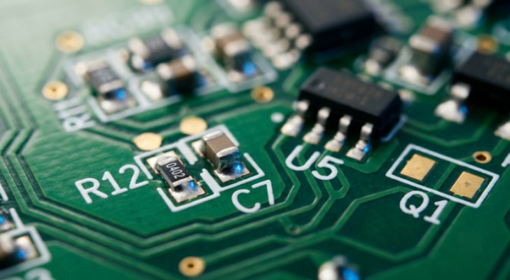
This process prevents a common mistake: a black three-terminal package appears to be a transistor, but it could just as easily be a protection diode. The label "R12" designates a component on the board but does not indicate the resistance value, manufacturer name, or part number for that component.
Contents
show
What Counts as a Circuit Board Component?
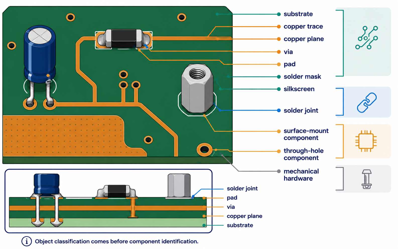
Components (placed parts) are connected to the circuit board and provide electrical or electromechanical functions for that assembly. The printed circuit board consists of a substrate, copper traces and planes, vias, pads, solder mask, and silkscreen. Pads are conductive landing areas used for component leads or soldered terminals; solder forms the physical joint, while a net represents the intended logical connection and its route may also include vias, planes, internal layers, and hidden branches. IPC terminology distinguishes the printed board from the printed board assembly. In the case of SMT and through-hole technology, the terms denote the mounting method used for each component; SMT devices connect to surface pads, through-hole leads pass through plated holes, and mixed assemblies can use both methods without defining the component's electrical role. Resistors, connectors, and diodes can appear in either SMT or through-hole forms. Mechanical items also require careful consideration when identifying electronic components. For example, an assembly may have a heat sink, shield, or standoff attached to it, but those items are not electronic components. Thus, these items should first be identified by what they connect to and what the drawing for that assembly designates the item to be.
Which Component Families Appear on a PCB?
It is not possible to define all the component families that can be connected to every PCB, as the family of components depends on the functions of the circuit board, including power conversion, signal conditioning, signal processing, timing, circuit protection, sensing, and connecting to the outside world. Component families are also grouped according to whether they are passive or active. Passive components typically include capacitors, inductors, and resistors, while active components commonly include transistors and integrated circuits or other semiconductor devices. While the classification system used here provides information about circuit behavior, it does not identify physical components based solely on their appearance. Even familiar passive components can have multiple functions depending on their placement on the circuit board and the type of circuit they are connected to (Integrated Passive Components in Micromodule SIPs).
The table lists possible component families, not their identities. For instance, a ceramic chip component could be a capacitor, a resistor, a ferrite bead, or a protection device. While ordinary MLCC chip capacitors do not have polarity, three-terminal low-ESL devices require the through and ground electrodes to be identified.
The circuit location will refine the component-family guesses. For example, a wound part that is adjacent to a switching controller and a power diode may belong to a converter, whereas a metal timing package that is adjacent to the CPU may provide that CPU's clock signal. Some relays combine an electrically driven switching element with physical contacts, whereas SSRs switch the electrical current using semiconductors. For electrical relays, see What Are the Basics of an Electrical Relay?
Can Shape and Color Identify a Part?
Shape, color, package type, and terminal count can eliminate impossible candidates. However, none of these alone confirms the part's function, pin configuration, or exact MPN. Because numerous unrelated manufacturers produce devices using standardized body outlines, molded body color can vary with the material used, component supplier, lighting, and production lot.
Round cylindrical cans could be aluminum electrolytic capacitors, crystals, sensors, fuses, batteries, or inductors. Check the area of the board around the part, lead arrangement, markings such as polarity or vent marks, printed code, and surrounding circuit. Silkscreen circular markings may indicate a keep-out area or the outline of the component. Black square parts with similar shapes may be microcontrollers, memories, sensors, voltage regulators, diode bridges, power modules, or transistor arrays; pin count, pitch, exposed pads, orientation marks, logos, and connected nets can narrow the candidates but do not confirm the exact device.
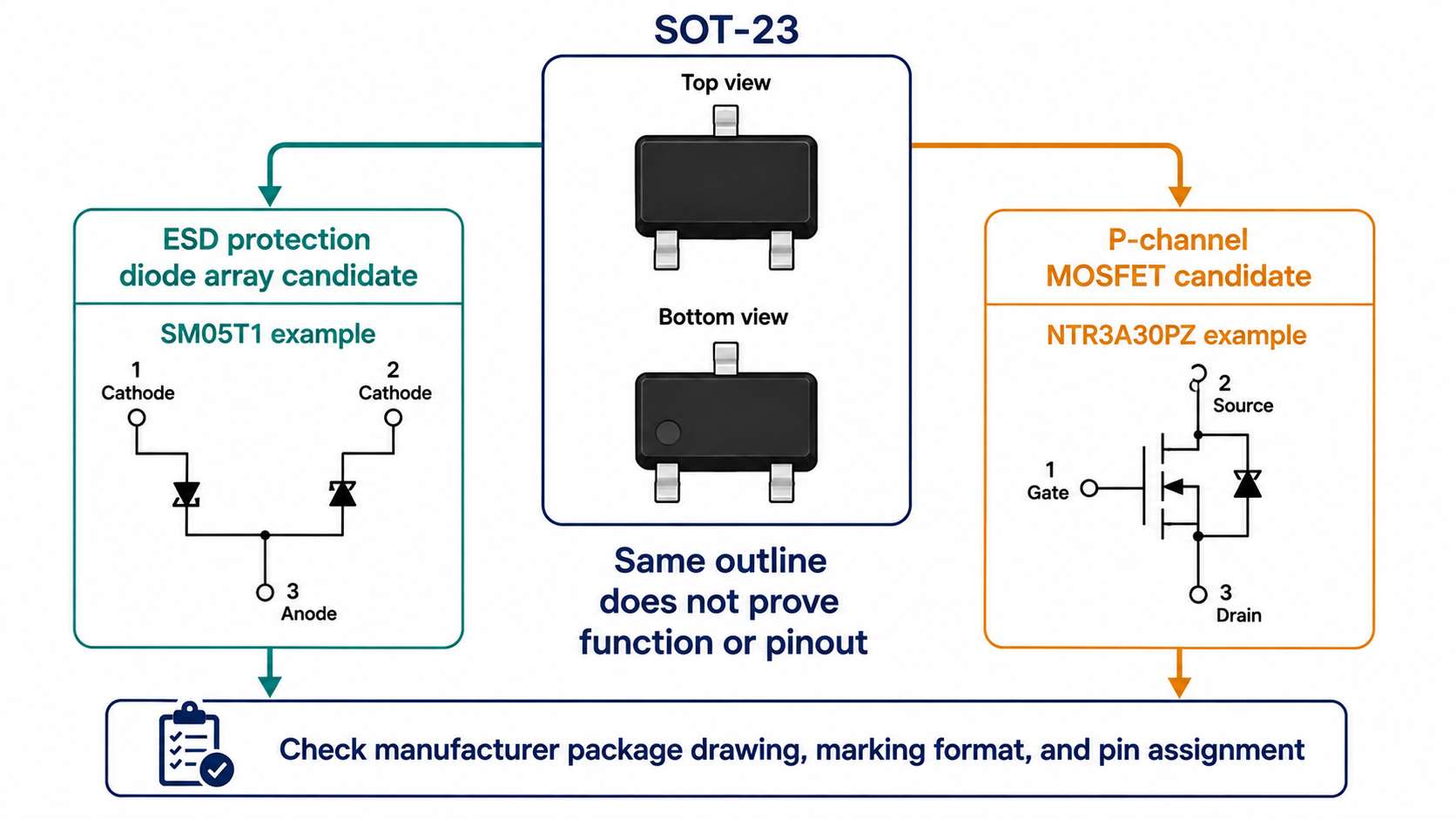
For example, onsemi makes both of these parts in the same outline (SOT-23). The SM05T1 ESD Protection Array and the NTR3A30PZ P-channel MOSFET are packaged in the SOT-23 outline; even though both are three-lead packages, this does not mean you can interchange the devices based on shape and outline.
Use the form and features of an SMD as a filter until you have compared the dimensions and geometries of the body, terminals, orientation marks, and other identifying features of several possible candidates. Once you do so, you can compare those candidates with the specific parts listed in their respective catalogs. Physical families such as SOT-23, QFN, and BGA describe package families, while the passive code 0603 is a size convention; therefore, neither is a definitive method of identifying an MPN, and the same digits can represent different nominal dimensions under imperial and metric conventions.
Reference Designators, Markings, and Part Numbers
Reference designators, value codes, top marks, manufacturing fields, and MPNs come from different sources; therefore, they do not all carry the same evidential weight and should not be treated as interchangeable, as doing so can turn a useful clue into a false identification.
Each reference designator identifies a component within the electronic schematic file (Schematic Editor 9.0), and reference designators can be reannotated during the design process. Therefore, the prefix and number that identify the design object (reference designator) must be appropriately interpreted based on the correct project revision, as reannotation can generate a new number for the design object (reference designator).
In general, the following prefixes are commonly used for a project's reference designators. The prefix does not define or determine the value or rating of the design item, nor does it define or determine the manufacturer or installed MPN. Instead, the prefix provides a means to identify a design item (reference designator) or a likely family of design items used in the design.
Top markings also require caution. TI has a lookup tool to determine the package markings or part numbers of TI parts, which is a TI-specific method and not a universal method for decoding all short codes on all products (Packaging Part Marking Lookup).
How Do You Identify an Unknown Board Component?
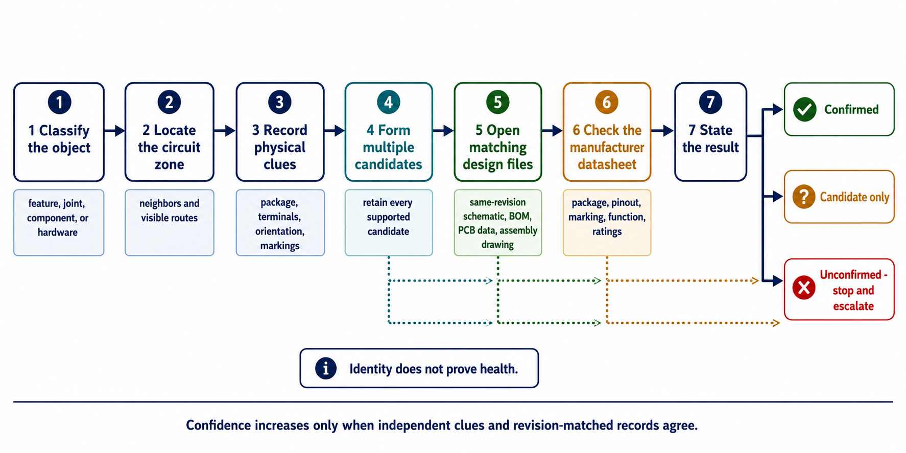
You should proceed level by level from observation to confirmation. The higher the level, the greater the strength of the conclusion you can draw. If there is a disagreement in the evidence, use the most strongly supported conclusion and not a guess.
- Determine the classification of the object as either a feature of the board, a solder connection, a mounted electrical component, or a mechanical component.
- Identify the circuit zone of the component and what function is assigned to the component on the board by determining if the zone is one that relates to power entry or conversion, processing, timing, sensing, isolation, RF, or external I/O; if applicable, note the proximity of the component to connectors, regulators, processors, isolation gaps, antennas, power devices, etc., and all of the visible pathways that exist to and from the component.
- Document as much physical information as is available about the component, including its physical dimensions, the number of terminals, the style of mounting, its physical orientation, any manufacturer's logo, the complete markings on the component, and its reference designator without translating or interpreting the markings yet.
- Retain all the candidates you have compiled based on your documentation of the component and the steps taken to gather supporting evidence.
- Locate and examine design files that correlate with the component. Check the schematic, BOM, PCB data, and assembly drawings for the same board revision. If the revision is unknown, document the missing revision information and which file or release identifier would resolve the issue.
- Review the manufacturer's datasheet related to the component. The dimensions, pinout, marking format, functionality, and relevant ratings of the package must match. The candidate will be eliminated if its pinout or package does not match the observed part.
- Be specific with the results reported. The results can be "confirmed," "candidate only," or "unconfirmed," with the supporting evidence for the selected determination.
Photographs should capture an overview of the entire assembly before taking close-up shots. Wide views provide context about the circuit and visible designators; close-up shots capture marking and terminal details. The entire board should be photographed, with the reverse side captured when it is safe and accessible. Rotating or enhancing the image may assist in revealing marking and terminal details; however, image processing cannot be used to recreate missing package, pinout, or revision evidence. Referencing the released BOM will provide information regarding what the engineer intended to install, while undocumented repairs may leave a compatible or incorrect replacement part. Therefore, confirming the installed part number should be based upon a match between the records, the physical component, and the corresponding datasheet.
Which Design Files Confirm the Part?
To achieve a precise identification of an installed part, the design records must agree on the following: location, value or description, footprint, package, part number, pinout, and revision number. There is no single design file that will have all of this information. Each of the elements provides unique but essential information through the schematic, PCB data, BOM, assembly drawing, and datasheet.
The schematic symbol expresses the function of the circuit and shows the logical connections to other components. The footprint associated with a schematic symbol contains the copper and mechanical mounting pattern of a component on a PCB. The physical package drawing contains information regarding physical dimensions and assigned terminal numbers for a component. KiCad notes that a given schematic symbol may have more than one possible footprint associated with it, which is why using the shape of the symbol alone is not a viable way to determine the package type (KiCad Schematic Editor 9.0).
The BOM maps the reference designators to procurement fields such as quantity, value, footprint, datasheet, DNP state, and custom MPN fields when the project includes them. The assembly drawing connects those records to the associated locations and orientation of the physical parts. A centroid or pick-and-place file can provide the reference designator, X/Y position on the PCB, board side, and placement rotation. However, these files alone do not confirm that the installed part was manufactured by the specific manufacturer being referenced, and the files must come from the same released revision before the mapping is treated as valid.
The Texas Instruments public AMC1204EVM User's Guide is an example of how to reconcile the records because it was produced as one controlled document containing the silkscreen drawing, schematic, and BOM. The next rows provide examples from that public evaluation board, not field data from a customer assembly.
Even though U1 and U4 are both components of the same functional family and are integrated circuits, their package variants differ. To know what row U1 and U4 fall into, you will use the reference designator; to determine what is intended for U1 and U4, you will refer to the BOM and the datasheet provided by the manufacturer; finally, to ensure that the intended device matches the installed part, you will inspect it physically.
When the Evidence Still Does Not Agree
When there are conflicting markings, revisions, packages, or pinouts for a device, the result must remain unconfirmed. If a part has illegible markings, you cannot confirm the device from those markings alone; and, if a part has an impossible pinout, you can remove this part from consideration as a candidate. There are instances of having an unknown revision of a circuit board, discrepancies between the BOM and the schematic, incorrect package dimensions, a lack of documentation, or evidence of undocumented repairs, and there is an inability to confirm a candidate based on the incomplete data set. There is nothing wrong with stating that you have identified two candidates almost equally, but one incorrect terminal assignment can cause you to classify a candidate device from plausible to impossible. If a top code for two manufacturers appears to be the same, it still cannot be confirmed as being the same device until you validate the logo, package drawing, functional usage, or design documentation of the actual device – until that point, preserve both candidates. Just because you can identify a device does not mean you can verify that it is healthy; a damaged resistor can be correctly identified, while a failed voltage regulator could have perfectly readable markings. To evaluate the overall health, you need to consider the circuit state, the expected measurements, whether you can isolate the device from parallel paths, and whether you are exercising appropriate safety precautions. Do not confuse unresolved identification with a generic methodology of live probing or multimeter readings. Take a brief record of all actions performed; clearly label the board's identification, revision, reference designator, observed markings, package measurements, part numbers of potential candidates, conflicting information, and what additional items are needed for ultimate confirmation.
From Confirmed Part to Assembly Handoff
Confirmed identities of components, to be usable as assembly data, must maintain the exact MPN, package, ratings, quantity, approved alternates, and revision of the board. All components that meet the criteria outlined above and have been verified as valid cannot be replaced with an uncontrolled substitution within either the purchasing or manufacturing process. The source file revision and reference range should be located next to the MPN, as well as the footprint, required ratings, polarity or orientation, quantity, and any approved alternate components, including their respective package, pinouts, ratings, and lifecycle checks. Even when components have visual similarity – two SOT-23 MOSFETs from different manufacturers sharing a common three-pin outline and common pin count – gates, drains, and sources can be connected to different physical pins of the same outline. Therefore, approving the use of another manufacturer's component based solely on the package and pin count does not provide the requisite information for producing an assembly, and installing such a component can result in an inoperable device after power-up or a short when energized. PCB assembly services manage the broader sourcing, placement, inspection, assembly, and production of circuit boards.
References & Sources
- Design To Manufacturing – IPC
- Schematic Editor 9.0 – KiCad
- AMC1204EVM User's Guide – Texas Instruments
- Packaging Part Marking Lookup – Texas Instruments
- SM05T1 Datasheet – onsemi
- NTR3A30PZ Datasheet – onsemi
- Use of Integrated Passives in Micromodule SIPs – Analog Devices
- Do Chip Multilayer Ceramic Capacitors Have Polarity? – Murata
- What Are the Basics of an Electrical Relay? – Omron