Upload BOM & Gerber

Using the term PCB is relevant only in the context of the electronics industry and may confuse individuals outside electronics, who may interpret PCB as polychlorinated biphenyls.
The primary function of the PCB is to provide stable mechanical support using insulating material and to provide electrical connections through copper conductors patterned according to the conductor geometry. Because a PCB allows for repeatable fabrication and assembly of the same design without using point-to-point wiring, the manufacturing conditions and costs associated with the PCB are controlled by the appropriate PCB manufacturing documentation; thus, the appropriate production files, inspection requirements, and quotation details are maintained.
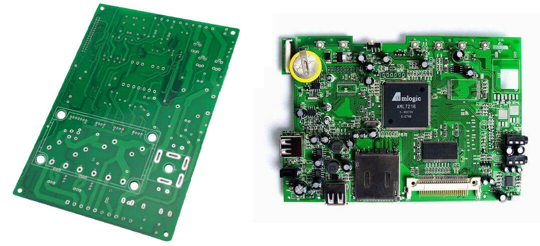
A PCB combines an insulating base with copper conductors, pads, holes, and features that connect different components. Thus, when referring to an unpopulated PCB, the appropriate term is “bare PCB,” while “assembled PCB” or “PCBA” should be used after all required components are attached. The term PCB, by itself, does not indicate whether any components, programming, testing, firmware, or accessories are included.
Contents
show
What Does PCB Mean in Electronics?
A PCB is a physical support for electronic components and routes electrical connections through copper conductors on an insulating material or structure. Without external components attached, the PCB is considered to be a “bare PCB.” A PCB determines the configuration and geometry of the copper conductors, attachment points, and holes, as well as the mechanical dimensions of the PCB. The PCB on its own cannot perform the complete function of the finished product (Analog Devices; Ansys).
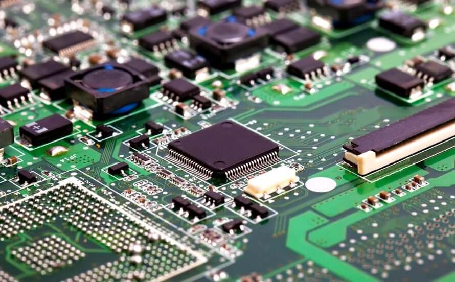
“Printed” refers to the process of repeatedly creating the conductor pattern on a PCB using imaging, plating, etching, or a similar process and does not mean that a desktop printer places working wires on the board. A PCB helps to reduce variation due to manual wiring from one product to another, supports automated assembly of PCBs, and allows the designer or manufacturer to control the relationship between spacing, impedance, and the return path from one production lot to another.
In day-to-day terminology, PCB and circuit board may mean the same thing. In some older standards and controlled documents, the term PWB is used. Because there are various informal terms and definitions of PCB, whenever the physical condition of the PCB determines the deliverable for a project, the drawing or purchasing document should use bare PCB, PCBA, or assembled PCB, with any project-specific term clearly defined.
The Visible Parts of a Printed Circuit Board
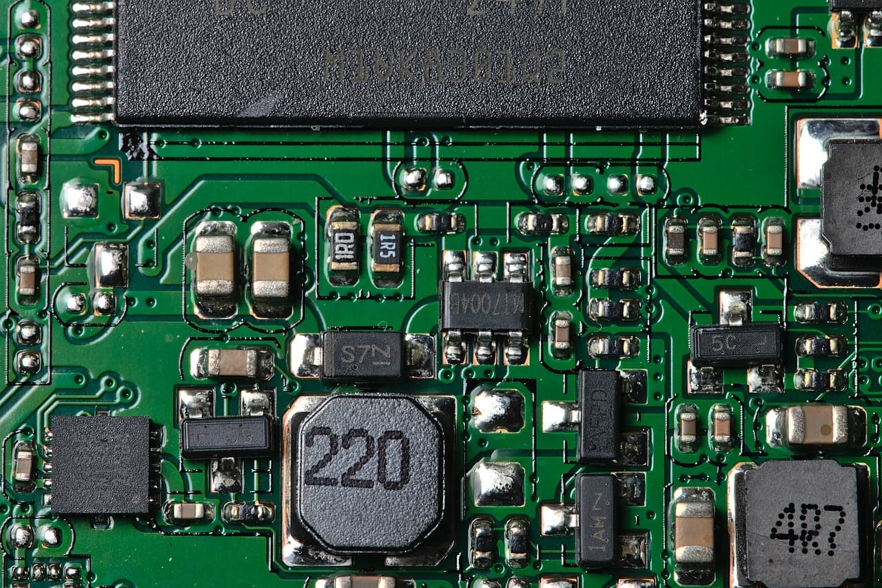
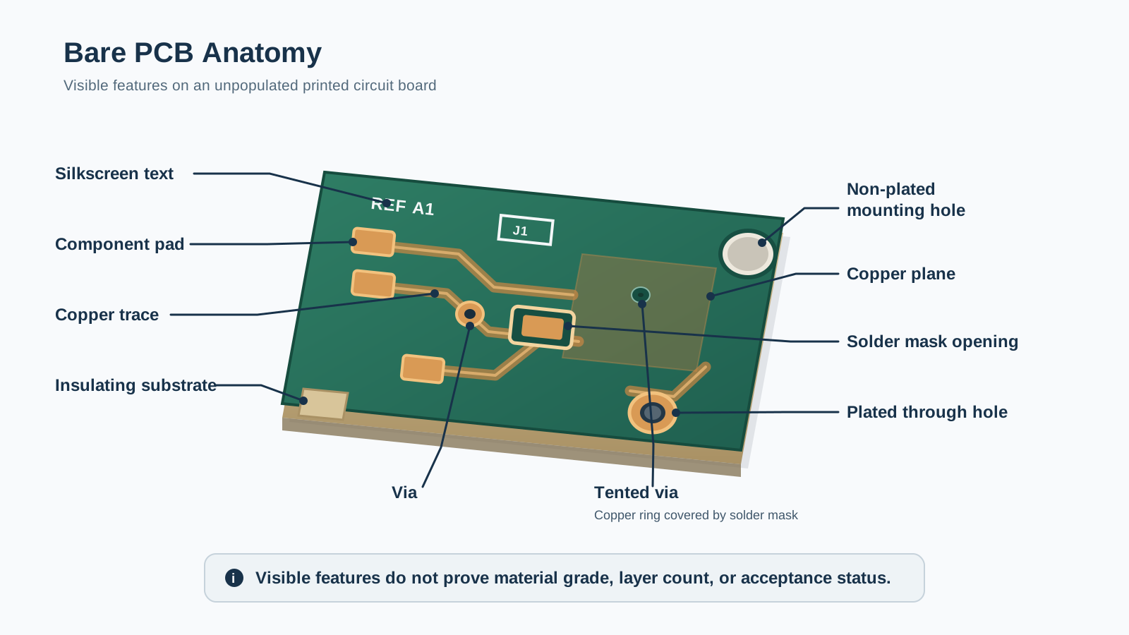
Visible features of a PCB are defined and categorized. Copper traces are conductive paths between electrical components; copper pads provide an interface for attaching wiring; vias connect conductive layers together; through-holes may accept conductive leads, mechanical fasteners, or support structures; a solder mask covers certain surfaces of the PCB; printed graphics indicate the orientation, connection points, and revision status of the PCB. Three-dimensional internal copper, buried vias, and embedded structures may not be visible from the board surface (SparkFun; Altium). Its electrical insulating properties come from its substrate material, which is commonly referred to as FR-4. Other substrate material options include polymers such as polyimide, metal-core materials, ceramic materials, and low-loss laminate materials. These substrate material options can change the physical properties of a PCB, including flexibility, heat transfer properties, dielectric characteristics, frequency performance, fabrication methods, and overall construction costs. Material descriptions do not only describe colour or stiffness; they also determine whether or not a PCB’s material type can withstand the electrical, thermal, and mechanical requirements of the end-product application.
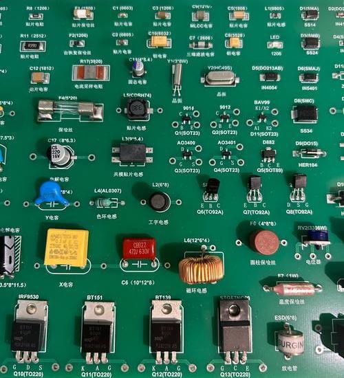
A pad is a conductive area of a PCB used to make specified electrical connections; for example, pads can be used for soldered terminals, press-fit contacts, test access, wire bonding, and other specified electrical connections. Vias connect copper on two or more layers of the board. Holes that have been plated or non-plated may be used for through-hole leads, fasteners, alignment pins, or other tooling features; therefore, two holes on the same PCB that look the same may not serve the same purpose.
The solder mask process is used to cover and protect most of the outer layer of copper on the PCB while exposing and allowing access for soldering to specific pads and features. A solder mask opening does not always expose bare copper; the exposed visible metal is typically protected by a surface finish such as HASL, ENIG, OSP, or ENEPIG applied to the exposed metal after the solder mask has been applied. The solder mask controls which outer-layer copper remains covered, while the surface finish protects the exposed copper and preserves its solderability. A via can also be tented, plugged, filled, or capped; therefore, having no visible hole does not necessarily mean that there is no interlayer connection (Altium, Mask Rule Types). Labels printed on the PCBs can be used to mark connector positions, component placements, polarity, revision status, warning notices, and traceability information. Printed labels do not conduct electricity, and the various colours of a PCB do not identify its electrical function. The same design can be made in various colours of solder mask or legend without altering its electrical performance.
How Does a PCB Carry Signals and Support Components?
A PCB carries signals as follows: signals, power, and reference connections are routed through copper traces; copper traces connect to pads; pads connect to traces or planes; and vias are used to connect traces or planes from one layer to another conductive layer. The printed circuit board maintains copper traces in fixed positions so that the spacing between components, routing geometry, and mechanical relationships remain repeatable between PCB designs (SparkFun; Altium).
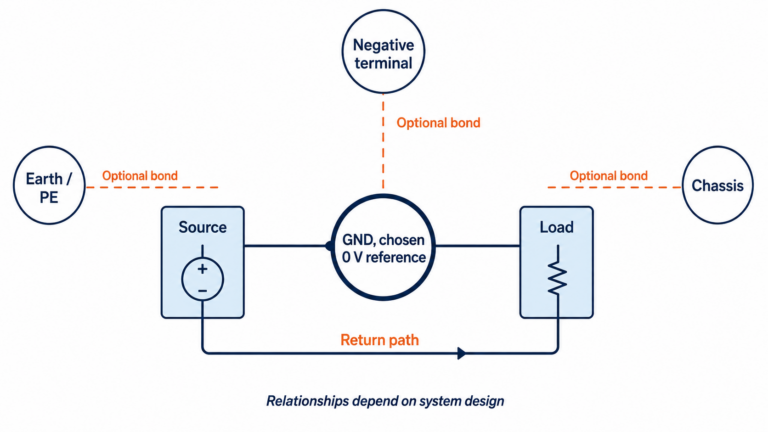
When a connector receives a signal, it travels from the connector pin to the pad, along the surface trace, through a via to the internal layer, and finally to the device pin. The surface trace is only one section of the overall path of the signal. Current will always travel in a continuous loop; the return path must be provided by a ground plane, power plane, or other nearby conductive material in order for the signal to return to its source.
When edge rates, current changes, or operating frequencies are high, the importance of a continuous return path is increased. A signal trace may have electrical continuity, but the presence of a split plane, the location of a layer transition, or a longer return path may contribute to additional noise, emissions, crosstalk, or signal distortion. The distribution of power generally requires the use of wider traces, copper pours, or planes, since conductor dimensions are influenced by current, voltage drop, heat, and return-path geometry.
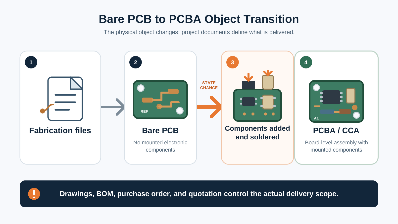
Copper paths, pads, vias, and connection holes are all considered to be in a “printed-board state.” To change a printed-board state to a board-level assembly state, specified components must be mounted and electrically or mechanically attached to the printed board.
What Is the Difference Between a PCB and a PCBA?
The major difference between PCB and PCBA for purchasing purposes is that the term “bare PCB” means a completed printed board, and the term “PCBA” means a printed board with all specified components. A PCBA is created by the addition of specified components to a bare PCB through surface-mount soldering, through-hole soldering, press-fit insertion, wire bonding, sockets, or conductive adhesives.
Advanced printed boards provide an important exception to the definition of a “bare PCB.” Advanced printed boards can consist of rigid boards with embedded resistive, capacitive, or active structures; distributed capacitive planes; metal cores; and other functional structures that are created within the board. The fabrication drawing and applicable specifications for advanced printed boards establish the governing definition of the product, even though no conventional component is visible on the surface (IPC-6012F).
IPC-A-600M provides observable acceptability conditions for printed boards; IPC J-STD-001J provides materials, methods, and acceptability criteria for soldered electrical and electronic assemblies. IPC-A-610J is commonly referenced for acceptability conditions for electronic assemblies. These documents differentiate between board fabrication and assembly workmanship; however, the drawings, BOM, testing requirements, and purchase records define exactly what is delivered.
PCB, PCBA, and CCA are used interchangeably in some cases; a supplier, engineer, or product label may use PCB when referring to a bare PCB, PCBA, or CCA. Therefore, to eliminate ambiguity, it is best to use bare PCB, PCBA, or CCA in the context of the project to define the product’s physical state.
Orders and quotations are used to resolve any remaining discrepancies. You should confirm whether the quoted price includes bare boards, electronic parts, assembly, inspection, electrical tests, functional tests, programming, conformal coating, mechanical hardware, serialization, and packaging.
What Can PCB Markings Tell You?
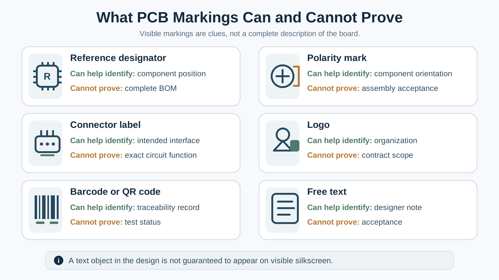
PCB markings indicate where components are physically located, their polarity, the location of connectors, revisions, brands, warning labels, or the traceability record of the product. PCB markings do not provide a full BOM, circuit behaviour, test results, material composition, or ordered deliverables. PCB markings may be indicated as text objects on a design layer but may not appear on the manufactured silkscreen for the PCB (Altium).
The letters R, C, L, D, Q, and U in a reference designator commonly indicate a class of component and its physical location; however, each company has its own naming convention. Polarisation markings indicate which direction the component is to be installed, connector labels indicate where the connections are to be made, and barcodes, QR codes, logos, date codes, or serial numbers indicate how to track the item. However, none of these markings indicates that the installed component is correct or that the board has passed inspection or testing.
The Inactive-Reserved IEEE/ANSI 315-1975 standard contains symbols for electronic diagrams and the letters used in reference designators. It can provide guidance on the various conventions for using reference designators, but it does not identify all of the labels printed on contemporary PCBs (IEEE).
PCB Types Depend on the Classification Axis
PCB types are identified by the attribute being classified. For example, single-sided means there is only one conductive layer, double-sided has two conductive layers, and multilayer is when more than two conductive layers are present. Rigid, flexible, and rigid-flex refer to the physical construction of the PCB.
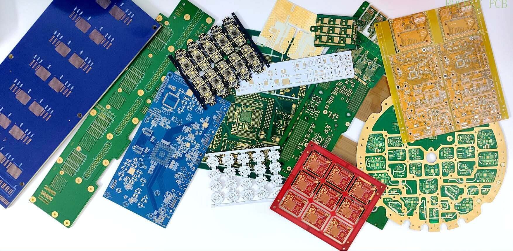
Some PCB types can fall into multiple classes. For example, a PCB can be multilayer and rigid-flex, or HDI and low-loss, as these terms refer to different attributes of the PCB. A compact wearable may use flexible construction with dense microvias, whereas a power-conversion PCB prioritizes copper capacity, spacing, and thermal paths. An RF PCB or high-speed data PCB should be constructed with controlled impedance, continuous return paths, and low-loss dielectrics as requirements. These classifications represent combinations of requirements, not alternative names in a single master list of PCB types.
Conclusion
To understand a PCB, you must first check three key elements: the physical object, whether conventional components have been placed on the PCB, and the predefined documents that define the product. The PCB is an insulating structure and contains conductive paths, pads, holes, and other connection geometry, while the PCB assembly is made up of the specified components and assembly operations. Markings provide visible clues rather than proof of material type, completeness, product quality, or functional capability.
When the next task involves schematic capture, component placement, routing, stack-up decisions, or design review, continue with PCB design services.
Once you know that your task involves component sourcing, assembly, inspection, programming, or functional testing, continue with PCB assembly services.
References & Sources
- Printed Circuit Board – Analog Devices — Analog Devices
- What Is a Printed Circuit Board (PCB)? – Ansys — Ansys
- PCB Basics – SparkFun Electronics — SparkFun Electronics
- Working with Pads & Vias – Altium — Altium
- Mask Rule Types – Altium — Altium
- Working with Text Objects – Altium — Altium
- IPC-A-600M, Acceptability of Printed Boards – IPC — IPC
- IPC-J-STD-001J, Requirements for Soldered Electrical and Electronic Assemblies – IPC — IPC
- IEEE/ANSI 315-1975, Graphic Symbols for Electrical and Electronics Diagrams – IEEE — IEEE