Upload BOM & Gerber

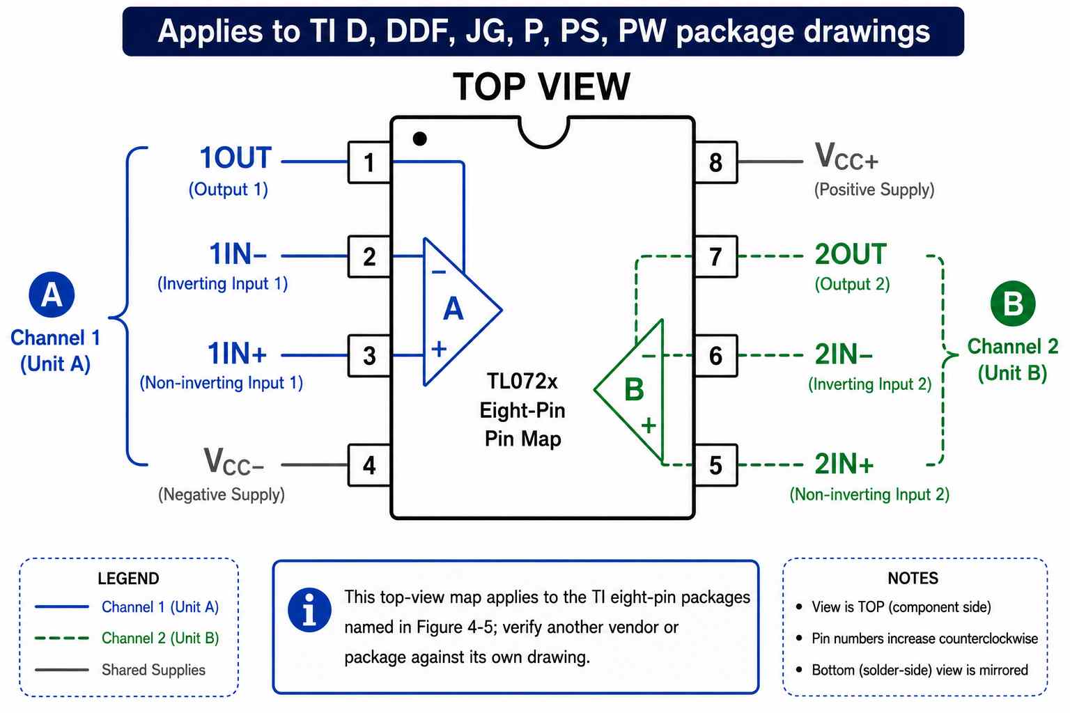
The TI eight-pin TL072x common top view shows that pins 1, 2, and 3 form channel 1, while pins 7, 6, and 5 form channel 2. Pin 4 is the shared negative supply, and pin 8 is the shared positive supply. This only applies once you have confirmed that the manufacturer, complete part number, package code, and drawing view match what is found in the datasheet.
Having just the base name isn't enough to ensure that you're referencing the right device. One TI document covers classic grades, the newer H family, and special M packages. Even if you are using the correct wiring, the circuit may experience clipping under invalid input, load, reference, or feedback conditions.
Contents
show
What Is the TL072 Pinout?
In a pin mapping for the two amplifier channels and shared supply rails of the common TI eight-pin TL072x top view, the following mapping is true. This mapping applies to TI packages D, DDF, JG, P, PS, and PW. All other packages must be separately validated against the TI TL07xx datasheet.
The TL072 is a dual op amp with JFET inputs. For each channel of the TL072, there is one non-inverting input, one inverting input, and one output. The signal connections for the two amplifier channels are independent; however, both channels share the supply rails.
In the application of the TL072 in either a dual-supply application or a single-supply application, pin 4 is specified as VCC− (negative supply). Therefore, for dual-supply applications where the TL072 is powered with both a positive and a negative voltage supply, pin 4 will be connected to the negative rail, not ground. In certain single-supply applications, pin 4 may be connected to ground.
ST has provided users of its TL072, TL072A, and TL072B products with the same functional order, but only within the package scope specified in its datasheet. The TI TL07x family of operational amplifiers provides users with TL071 (single), TL072 (dual), and TL074 (quad). However, the TL072 eight-pin package does not expose offset-null pins, and hence it is not advisable to transfer any offset-null connections from the TL071 to the TL072 package.
Which TL072 Do You Actually Have?
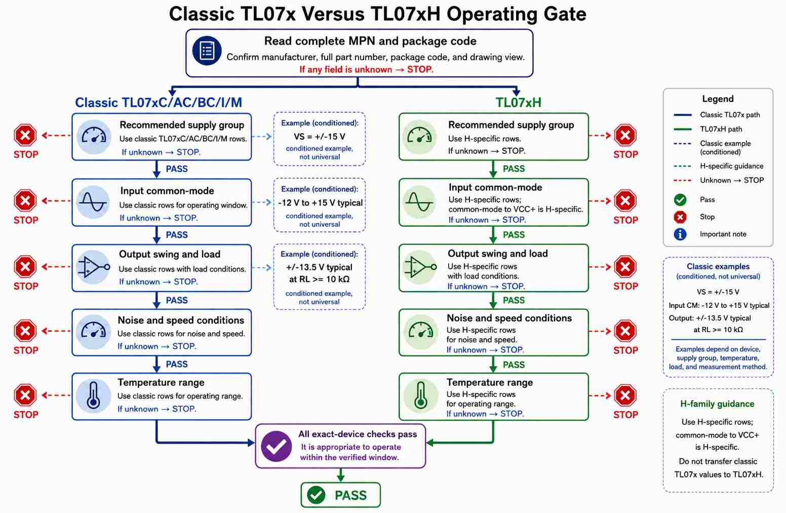
If you are not certain of any of the four fields listed above, do not build a functional map for the TL072 you have. The TL072 is a general identifier for a larger product family produced by multiple manufacturers and is not limited to one specific package or one specific electrical specification.
The TL072M from TI has two very different package configurations. The "U" package is a 10-pin Chip Flat Package, where pins 1 and 10 are designated "NC"; however, pins 2 through 9 are used for active function connections. The "FK" package is a 20-pin Leaded Ceramic Chip Carrier whose functions are mapped to the lead numbers associated with it. This can be seen in Figures 4-6 and 4-7 (TI TL07xx datasheet). It is incorrect to state that the "TL072 is always an 8-pin IC."
The letters A, B, H, or M do not have one cross-vendor definition or interpretation; for example, while TI labels grade/generation members of its TL07xx family as A, B, H, or M in Rev. W, ST uses separate order codes for its products.
According to TI, the TL07xH is a next-generation product of the TL07x series and H is not merely a designator for a different packaging style (TI TL072H product page). In multi-device datasheets, values for each device must be qualified by group, package note, and test conditions.
How Do You Read the TL072 Top-View Pin Map?
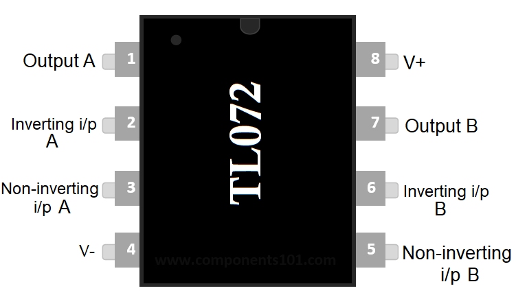
To determine the pin configuration of the TL072, first locate the "notch" or the pin 1 dot as shown in the datasheet. When looking at the device from the top view per the datasheet, begin counting pin numbers counterclockwise starting from pin 1. The notch would be at the top of the device. Starting with pins 1 through 4, they will run down the left side, while pins 5 through 8 will run up the right side. The pin positions will appear mirrored when viewed from the solder side of the device.
When reading a schematic, each amplifier circuit (e.g., U1A) is represented as an individual unit. For U1A, the pin numbers are represented using 1/2/3, while U1B pin numbers are represented by 7/6/5. The 4th and 8th pins are the power pins for both circuits. When determining feedback connections, do not rely on the position of the triangle; symbols can face either direction.
The plus and minus labels indicate the "differential" polarity. Negative feedback connects an output-dependent signal back to the inverting input; the non-inverting input receives either a reference voltage or the input signal. Different channels may be used for different functions. For example, one channel may provide "buffering" functions while the other may function as a "filter." The label for the unit is still very important; you cannot connect pin 2 of U1A to pin 6 of U1B just because pins 2 and 6 are both inverting inputs.
There are two ways to check how pins are oriented: by using the package drawing for pin 1 in physical space and by checking the library for pin numbers for U1A, U1B, and power. The left and right sides of the package drawing alone cannot provide this information.

What Does the TL072 Pinout Look Like in a Real Circuit?
For channel 1 of an inverting amplifier, the input signal comes into pin 2 through an input resistor; the output from pin 1 comes back to pin 2 through a feedback resistor, and the reference voltage connected to pin 3 is typically set at a predetermined reference value. The reference could be 0 V with dual-supply operation, but with a single supply, the reference could be a "virtual midpoint." With a single supply of 12 V and pin 3 set to a 6 V virtual midpoint, a 10 kΩ resistor connected to pin 2 and a 100 kΩ feedback resistor connected from pin 1 to pin 2 give a gain of -10. Therefore, a 200 mVpp input will produce a 2 Vpp swing centered around 6 V on pin 1. This should be sufficient to remain within the acceptable range of a 12 V rail; however, the same resistor values on a 5 V rail will exceed the allowable output voltage swing of the TL072. Channel 2 will be connected to pins 6, 7, and 5 of the TL072. The pin numbers of the device are relatively simple, but the reference voltage, resistor ratio, and expected output must always stay within the specified limits stated in the TI TL07xx datasheet.
For example, in the case of a high-impedance sensor stage, such as a piezo pickup or photodiode with a source impedance in the range of hundreds of kΩ to MΩ, this configuration relies heavily on the picoamp-level bias current of the JFET input. If you were to use a bipolar op amp in this same socket, it could load that source and thus change a clean DC baseline into a drifting offset.
When using an active filter, the feedback network's resistor and capacitor values determine the corner frequency, while the speed of the active filter is governed by the TL072's around 3 MHz GBW and 13 V/µs slew rate (5 MHz GBW and 20 V/µs slew rate for TL07xH). Though a multi-kHz audio filter fits well within this design area, anything approaching the hundreds of kHz requires closer checking against these limits.
When using a buffer stage, the buffer stage's own input impedance isolates a high-impedance source, such as a potentiometer wiper above 100 kΩ, from the subsequent load and helps prevent attenuation of the input signal; the input impedance of the buffer, and not the pin map, determines that isolation.
A mixer or preamplifier stage can add noise from every input resistor associated with its summing network; as more inputs are summed, it also needs more output-swing headroom to prevent clipping.
Supply Pins Are Correct Only Inside the Operating Window
Connecting the power supply connections (pins 4 and 8) of the TL072 is just the first step of the supply verification process. In order for the selected part to meet the supply requirements of its recommended range, you must verify that the common-mode limit for inputs, output swing, and temperature limitations are met. The fact that you are operating a TL072 using a single supply does not imply that all inputs and outputs of the TL072 can reach zero volts.
TI Rev. W groups devices and packages by their recommended span of total supply values for that specific device/package. For example, it specifies that 10 V – 30 V are recommended for NS/PS packages and TL07xM, while other devices that it covers are specified to have 4.5 V – 40 V. For classic devices, Section 8.3 warns that they may be permanently damaged above a 36 V single supply or ±18 V dual supply.
While both statements describe supply-voltage limits for certain devices and their intended applications, the statements should not be interpreted as a universal limit for all TI TL07xx products.
A virtual midpoint can serve as a signal reference between power supply rails for a single-supply design; it will not change pins 4 and 8 of the chip. A virtual midpoint does not increase the common-mode or output limits of the circuit, although the actual input and output must be limited with respect to the rails and the load. Virtual-midpoint bias makes a DC operating point possible but does not guarantee that the rest of the circuit has acceptable source loading, drive characteristics, closed-loop response, and stability.
Why Can Correct Pins Still Produce the Wrong Output?
There are two classes of likely faults that will result in an incorrect output. Mapping Faults refer to a mapping problem, such as a mirrored view, crossed channels, or mismatched library numbers, while Operating Faults refer to problems related to the rails, common-mode, headroom, load, and feedback.
To verify that the device is functioning correctly before replacing the chip, perform the following steps:
- Read the complete device marking and package code, then compare them against the manufacturer's drawing.
- Verify that the top-view orientation matches the manufacturer's drawing and continuity exists from each package pin to the proper net.
- Measure VCC+ at pin 8 and VCC- at pin 4 referenced from the selected reference point.
- Compare the input voltage on the input pins with the common-mode limit for the specified device.
- Compare the requested output voltage against the load-conditioned output range.
- Trace the negative feedback path of the active channel to verify that it provides the expected closed-loop gain.
- Use a known small signal only after verifying a DC operating point.
With a common-mode violation, the output may saturate despite correct continuity. A heavier load will clip the output sooner than a lighter load for the same reason: with a ±15 V supply, the classic TI output swing is typically ±13.5 V into a 10 kΩ load and ±10 V into a 2 kΩ load, so a target close to the rail that has worked with a light probe load will clip when the actual load is connected — this invalidates the assumption that the output "should reach the rail" (TI TL07xx datasheet).
An amplifier that lacks a return path is left open loop; cross-channel feedback creates another circuit. Verify physical nets. Do not assume proximity between a schematic connection and the physical connection.
When a measurement violates a qualified row, correct that condition before replacing components or adding compensation, rather than replacing an IC on the assumption that the IC pin mapping is at fault.
Set Up the Unused Channel, Bypass, and First Power-Up
Before turning on power for the first time:
- Close the unused amplifier in an appropriate linear configuration, provide local decoupling capacitance at the supply pins, and test an active channel using a defined, controlled signal and light load.
- The first power-up process should be consistent with Analog Devices' guidelines for closing unused op amps using stable feedback loops within the common-mode range specified by the manufacturer (Analog Devices unused op-amp guidance). It is best to choose a TL072 reference that can provide a valid output; do not float the inputs or tie them blindly to a rail.
- TI recommends using a 0.1 µF local bypass capacitor and keeping sensitive input or feedback traces short (TI TL07xx datasheet). Long traces increase parasitic impedance and can create coupling that is not apparent from the schematic.
First Power-Up Sequence
- Do not apply power during the orientation check, continuity check, feedback check, and check for the unused circuit.
- Apply a current-limited supply to provide the requisite supply voltage as recommended by the manufacturer for the specific device.
- Measure pins 8 and 4 before drawing any conclusions about the proper operation of the device.
- Measure the DC voltage on each input and the active output.
- Apply a small signal that stays clearly within the input/output ranges that have been verified.
- Measure gain and output DC offset using a known light load.
- Use the appropriate test equipment to assess overshoot or ringing, considering the defined load condition.
Capacitive loading can lead to decreased phase margin, which may lead to ringing in output stages. Some degree of isolation at the output may help, but how much isolation is required is determined by the amplifier, the closed-loop gain, the load used during testing, and the layout of the circuit. TI's training does not support a universal TL072 isolation value.
Can NE5532, LM358, RC4558, TL082, or LF353 Replace It?
No, there is no universal "drop-in" replacement for the TL072 based solely on the standard eight-pin function map of these various integrated circuits. Some packages may be physically compatible with the TL072, but each device must be considered as an electrical replacement for the TL072 based on input circuit design, maximum source impedance, supply range, input/output signal range, noise level, speed of response, output load, stability, temperature, and other package details.
Although the NE5532 has lower typical voltage noise than the TL072 for low-impedance sources, its higher input bias current makes it less suitable for applications operating at high source impedances. As such, its roughly 200 nA input bias current can become a liability above about 50 kΩ source impedance, producing DC offset and injected current noise in high-impedance sources such as piezo pickups or photodiodes, so it does not provide the same flexibility as the TL072. (TI NE5532 product page)
In particular, while the LM358's GBW is typically rated at 0.7 MHz with a 0.3 V/µs slew rate, the TL072 has a GBW of approximately 3.0 MHz and a slew rate of 13 V/µs (or 20 V/µs for TL07xH). You may experience slew-rate distortion at frequencies above about 95 kHz for a 1 Vpp signal. (TI LM358 product page)
Even though the input common-mode range of the LM358 allows for operation down to the negative rail, it does not compensate for its lower typical GBW or slew rate compared with the TL072; therefore, the LM358 would not be acceptable for use in applications where either of these elements is critical in determining your circuit's performance. As the RC4558 is a bipolar-input device, it requires similar consideration for high source impedances as the NE5532 and LM358. Its filter-design behavior still needs to be checked against the TL072 requirements (TI RC4558 product page). The TL082 and LF353 are also dual JFET-input devices that share the same pinout and have picoamp-level bias current; however, the TL082 and LF353 differ from the TL072 in several respects. Each component has varying levels of offset drift and noise characteristics; therefore, if a TL082 is substituted for one of the TL072 grades without consulting the matching table, it is possible for the TL082 to be outside the original design's offset budget (TI TL082 product page; TI LF353 product page).
Using the pin numbers alone to demonstrate functional layout compatibility will not guarantee equivalent characteristics in noise, headroom, startup, overload, or stability.
Carry the Pin Numbers into the Symbol, Footprint, and BOM
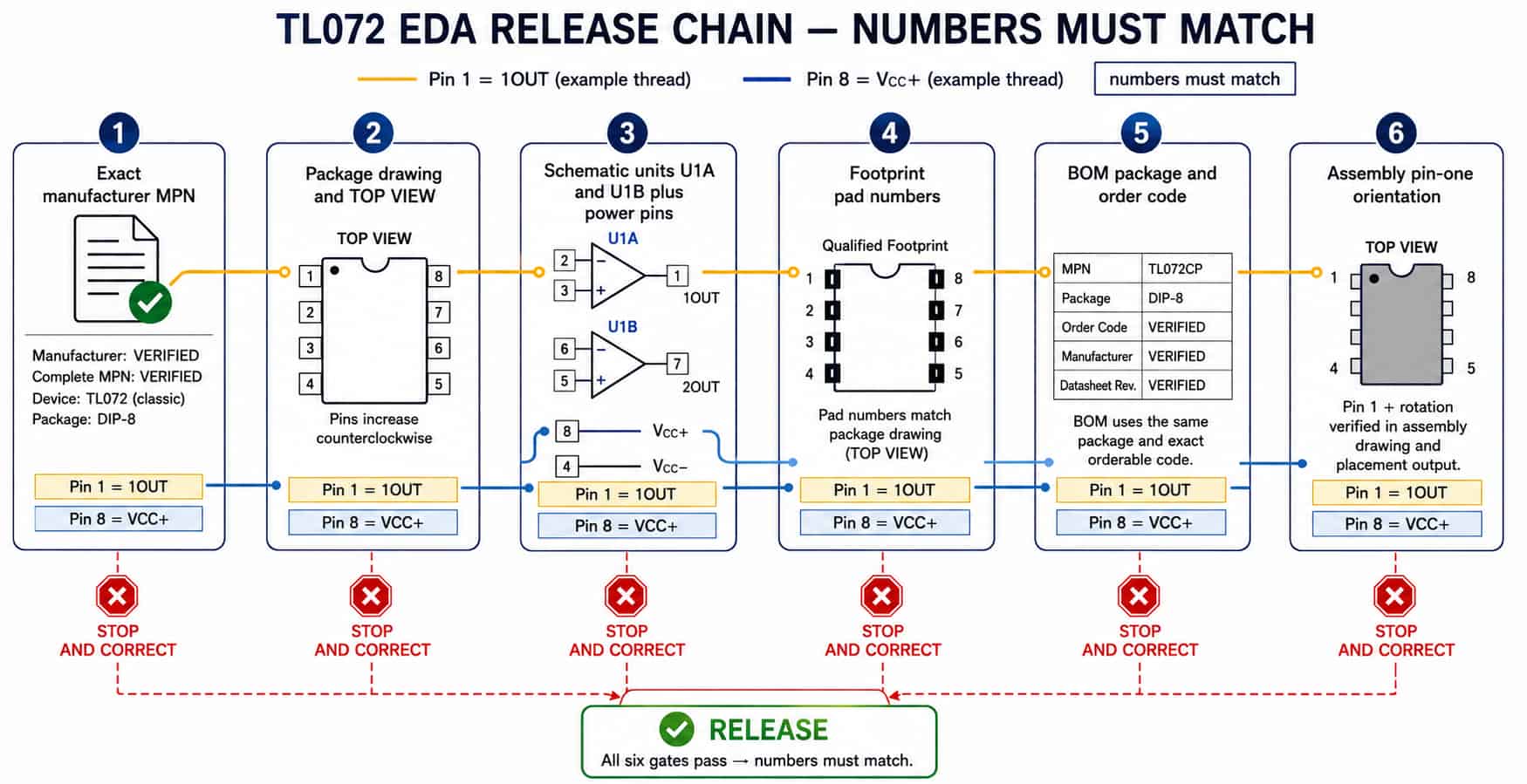
Verify that the pinout elements are associated correctly, including the datasheet function, symbol pin, footprint pad, BOM part and package, and assembly pin-one orientation.
The KiCad Schematic Editor associates symbol pins and footprint pads by their respective pin numbers. U1A and U1B identify the units, but the actual physical mapping follows the pin numbers, including any separate power unit.
To verify your component's identity, follow this order of checks:
- Lock in the manufacturer, MPN, package code, and approved datasheet revision.
- Open the package drawing and determine whether it is a top or bottom view.
- Verify that the U1A, U1B, and supply pin numbers in the schematic library match the actual physical layout.
- Compare all symbol numbers with their respective pad numbers for accuracy.
- Verify pad 1, the outline of the component body, and the orientation marking on the PCB.
- Ensure that both the BOM description and order code match the same package type.
- Check pin 1 and rotation in both the assembly drawing and placement output.
To be able to properly verify a component, the BOM should keep all of the identity fields together. A BOM line indicating only TL072 does not provide adequate information to determine whether you are ordering the correct package type, while a generic footprint may hide a mirrored-view error.
Before manufacturing the PCB, do one last check to verify the footprint and pin-one orientation and to see whether you have access to the component for testing. However, this step should not replace pin-by-pin verification.
Conclusion
When using the TL072, a reliable reference pinout is more than simply an eight-pin diagram you remember; it must be confirmed that you are using the correct manufacturer's part and package, that the signals operate within the defined operating window of the component, and that the footprint pad numbers, BOM, and assembly orientation are consistent.
Once all of the identity fields are the same, validate your circuit either through a controlled first power-up test or prototype test. If any item is outside the specification, correct the mapping or operating conditions before replacing the IC or attempting to find a substitute for it.
References & Sources
- TL07xx Low-Noise, FET-Input Operational Amplifiers – Texas Instruments
- TL072H Product Page – Texas Instruments
- Low Noise JFET Dual Operational Amplifiers – STMicroelectronics
- Avoiding Noise and Power Problems with Unused Op Amps – Analog Devices
- Capacitive Loads – Texas Instruments
- NE5532 Product Page – Texas Instruments
- LM358 Product Page – Texas Instruments
- RC4558 Product Page – Texas Instruments
- TL082 Product Page – Texas Instruments
- LF353 Product Page – Texas Instruments
- KiCad Schematic Editor – KiCad