Upload BOM & Gerber

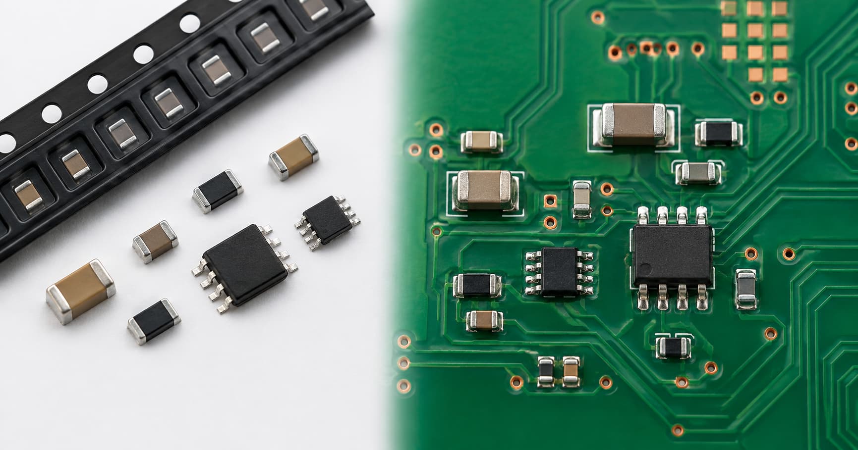
SMT meaning in electronics refers to Surface Mount Technology, which uses the surface of a PCB to attach the metal terminations of an electronic component to the lands or pads on the surface of the PCB. A PCBA is an assembled PCB.
SMT describes the attachment method; however, other materials, processes, inspection and testing standards, and acceptance criteria must be documented separately.
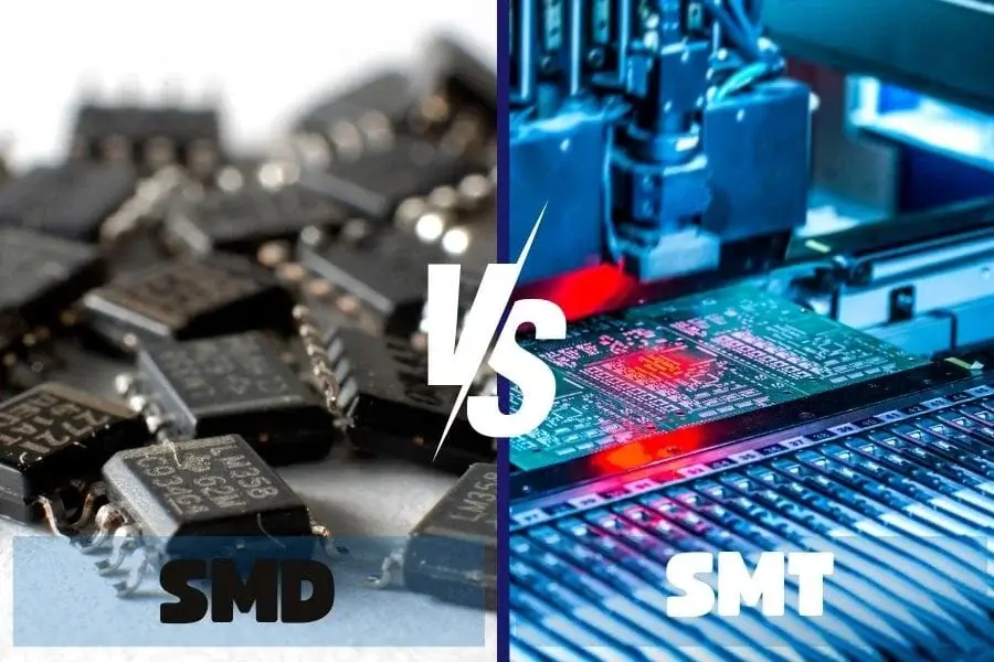
- SMT is the attachment method; SMD is the device type; PCBA is the completed assembly.
- The SMT process typically includes solder paste printing, component placement, reflow soldering, and pre- and post-assembly inspection and testing.
- The choice of SMT, through-hole, or mixed assembly depends on the component’s physical size, mechanical configuration, thermal requirements, electrical characteristics, and the circuit board’s inspection and repair requirements.
Contents
show
What Does SMT Mean in Electronics?
SMT is used to create connections between the lands of a PCB and the terminals of an electronic component. Through-hole technology allows the electrical leads to pass through plated openings and then be soldered to the circuit board. SMT and through-hole both create electrical and mechanical connections; however, each requires different features on the circuit board and uses different methods of assembly.
No single machine or soldering technology defines SMT. While reflow processes are the most common for building SMT assemblies, there are other ways to attach surface-mount components, including wave soldering, hand soldering, HBA, or other qualified methods.
Just because SMT components are mounted on the surface does not mean all terminations are completely visible. SMT boards use a variety of holes for signal, ground, thermal, tooling, or mechanical mounting, and mixed technology can include leaded connectors or magnetic components. Package terminations can also be hidden underneath BGA, QFN, or exposed-pad devices. Therefore, the term “Surface Mount” describes the relationship between the component and the surface lands of the circuit board rather than accessibility to inspection or repair points.
The rapid expansion of SMT occurred during the 1980s when components became smaller and could be placed at higher density using automated assembly equipment. However, through-hole technology was still useful, and mixed technology developed using both mounting methods.
SMT, SMD, and PCBA: Naming the Right Layer
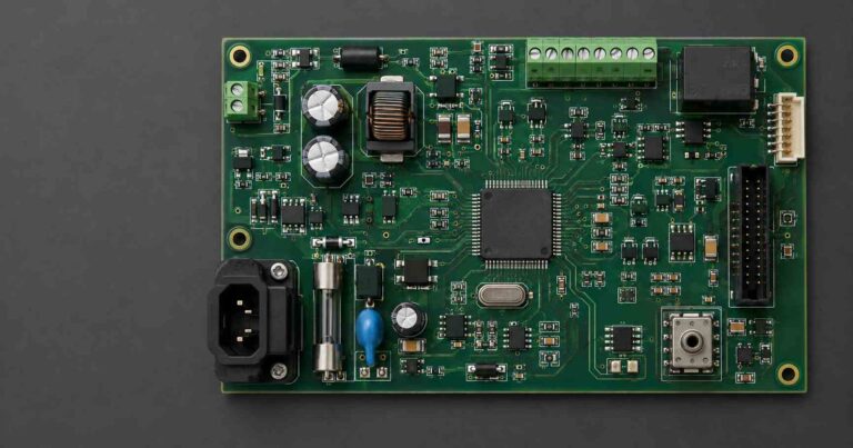
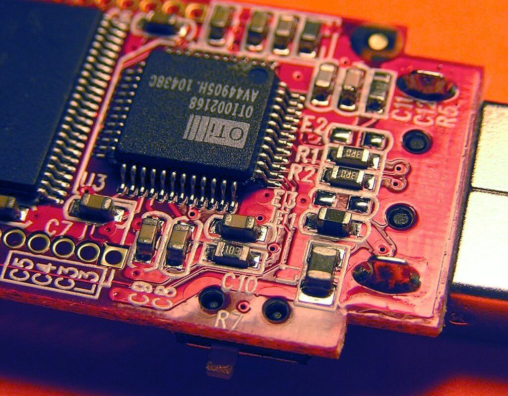
A PCBA features both SMDs and through-hole components, thus allowing one common term for describing the assembled board regardless of which mounting style is used. To illustrate this concept, consider a PCB. It could contain a QFN controller, chip-passive components, and through-hole connectors, as well as wires soldered manually on the board surface. All of these items could be combined in a single PCBA and still retain the PCBA designation.
Describing a part as an SMD does not define the land pattern, polarity, moisture sensitivity level, exposed pads, reflow limits, or access for inspection associated with that part; these conditions would typically be defined by the manufacturer’s part number and associated package documentation.
How Does the SMT Process Work?
The processes involved in producing SMT assemblies typically consist of preparing the PCB, solder paste, stencil, components, machine programming, and anything else needed before placing the parts onto the PCB. The materials selected and the settings used for the SMT assembly process must correspond to these inputs, including the board finish, package families, solder system, product risk, and acceptance requirements.
Solder Paste Printing
The solder paste is applied onto the PCB using a stencil. The amount of solder paste applied and the location on the PCB where it is deposited depend on the geometry of the stencil aperture, stencil thickness, the condition of the paste when it is printed, the design of the pads, the support of the PCB during printing, the printer settings, and the distance between the stencil and the PCB when the solder paste is printed. There are various types of SPI, which measure the height, area, volume, or offset of the solder paste that is printed before component placement. Inspection can allow for early identification of printing deviations; however, inspection pass/fail criteria and limits must be established based on each product and process.
Errors occurring during printing influence subsequent defects. Insufficient solder paste may contribute to unconnected pins or inadequate solder-joint connections; excessive or poorly contained solder paste increases the risk of solder bridging, solder-ball formation, or voids occurring in exposed pads. Furthermore, the amount of solder paste may not be uniform across the two ends of a chip component, and this may also contribute to tombstoning. SPI is performed on the solder-paste deposit before the reflow process, and while it allows for early identification of printing deviations, it cannot by itself demonstrate that the finished solder joint meets electrical, mechanical, and thermal requirements.
Component Placement
Component placement equipment aligns devices to the PCB footprint using information provided by the BOM, feeder assignment, component orientation, and centroid data, as well as camera settings and package geometry. Errors in placement can occur due to incorrect information in the BOM, improper setup of feeders, incorrect polarity designations, incorrect nozzle selection, errors in matching the package geometry to the library, and errors in the program for the placement equipment. All of these factors require verification using FAI or automated inspection to confirm that the device has been placed correctly.
When the component is placed on the PCB and the solder paste melts during reflow, the surface tension of the solder causes limited self-alignment of the component with the solder-paste-covered pads. The surface tension of the solder cannot correct errors in either the component type or orientation, nor can it correct a mismatched footprint or excessive deviation from the intended placement point. Thus, the results of the placement operation will be evaluated in conjunction with the BOM, package library, feeder map, and first-article evaluation, and not solely attributed to machine accuracy.
Reflow Soldering
Reflow soldering is a controlled heating cycle that activates the flux, melts the solder alloy, allows for wetting of the solder joints, and cools the assembly. The reflow profile used must be determined by examining the specific material types, including paste chemistry, package limitations, PCB thickness, copper distribution on the PCB, the weight of components being placed, and the amount of product being processed in the oven (oven load). In addition, a semiconductor package should not be evaluated independently of the PCB design, solder paste, handling, and reflow conditions.
The peak temperature of a qualified reflow profile alone does not define the qualified reflow process. The heating rate at which the assembly is heated to its peak temperature, the thermal uniformity across the PCB and package, the time above liquidus temperature, the temperature differences between the multiple components on the PCB, and the cooling behaviour of the assembly will all influence wetting, warpage, intermetallic formation, and the exposure time of the components during the reflow soldering operation. Various oven recipes may yield varying board-level results due to differing thermal-conduction paths, weight distribution of components, position of components on the PCB panel, or the total amount of product being reflowed through the oven.
Inspection and Testing
Inspection evaluates particular characteristics relating to the physical and workmanship aspects of the soldering process. Various inspection methods include evaluating printed solder paste deposits using SPI, evaluating component placement and solder characteristics using AOI, and verifying hidden solder joints or bottom-side thermal-pad solder areas using X-ray inspection techniques. Electrical testing will verify specified circuit connections or values against the product specifications. Furthermore, functional testing will determine how well the product functions according to the expectations outlined in the product specifications. Each individual inspection or testing method provides unique information and therefore cannot substitute for another inspection or testing method.
Therefore, just because one inspection or testing method has passed does not imply that the other methods would also pass. A passing SPI result alone does not demonstrate the successful formation of a post-reflow joint; a good AOI image does not verify a concealed BGA connection; and acceptance of X-ray imaging does not establish electrical capability or operating temperature for that specific connection. Therefore, any inspection or test evidence used to demonstrate a particular risk must be matched to the specific physical or functional risk being examined.
Stencil design and acceptance standards have different purposes. IPC-7525C indicates that stencil printing performance depends on several variables, which means that there is no one stencil rule that can be equally applied to all assemblies. J-STD-001J addresses soldering processes and materials, while IPC-A-610J addresses post-assembly acceptability of assemblies. Therefore, both the applicable documentation and acceptance class must be explicitly stated and not implied by using the term “SMT.”
What Are the Advantages and Limitations of SMT?
Component Density / Double-Sided Assembly
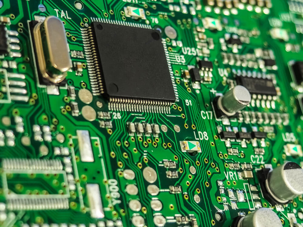
Surface mounting allows for smaller component packages, closer spacing of component terminals, and placement of components on both sides of a PCB. These advantages can lead to reduced PCB area or more functions within the same overall dimensions.
However, component density is also restricted by available space for escape routing, thermal spreading, test access, assembly clearances, package height, and rework area. Double-sided assembly does not mean that any arbitrary amount of component mass can be placed on either side; joint geometries on the first side of an assembly, component mass, molten-solder surface tension, shadowing, and exposure to a second reflow cycle will all influence the assembly sequence.
Automation and Process Repeatability
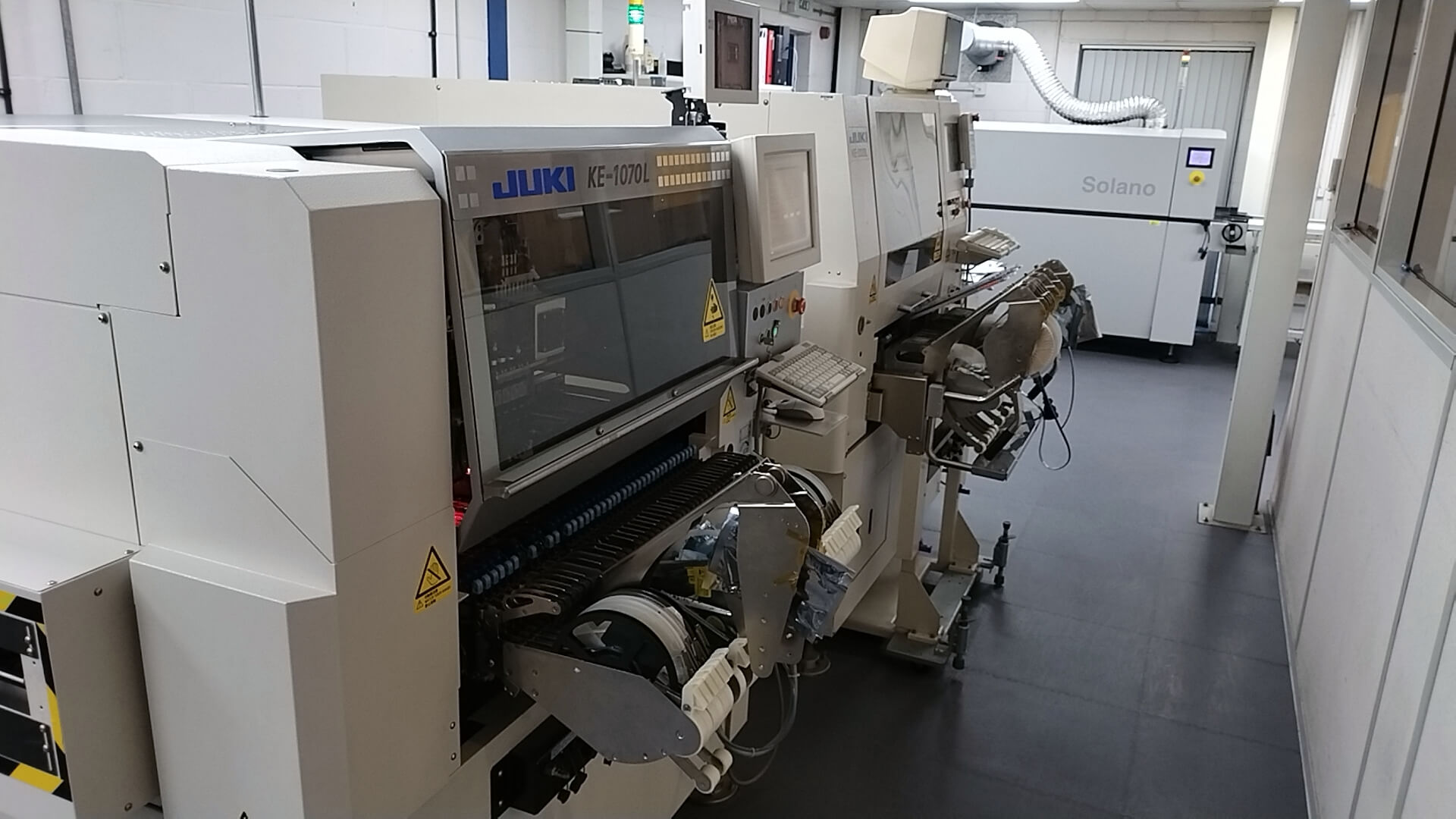
Stencil printing, automated placement, and conveyorized reflow processes allow the production of repeatable parts at acceptable volumetric production rates. However, automation does not eliminate the setup and process risks associated with incorrect feeder assignments, variation in paste transfer, placement-machine calibration, errors in package libraries, and the use of improper thermal profiles; these risks can affect multiple assemblies before a defect is identified. To achieve repeatability, the inputs to an automated process must be controlled, monitored, and verified rather than relying solely on automation.
Electrical Performance
Parasitic inductance, parasitic capacitance, and loop area may be reduced in certain circuits by having smaller terminations and compact layouts; however, there is no assurance that SMT will achieve higher frequency or better signal integrity. Ultimately, the electrical characteristics are determined by the package model, stackup, return paths, grounding, routing, transition method, and termination strategy used.
The manner in which a package connects to its PCB may also influence its performance. A short-termination QFN or BGA could experience poor performance if the return currents encounter gaps in the return path, if vias create discontinuities, if there is a weak ground connection, or if the connector launch represents the dominant electrical path within the channel.
Inspection, Repair, and Mechanical Loads
Small joints and bottom-terminated packages present challenges for inspection and rework. AOI, X-ray, microscopes, and electrical testing may be necessary to inspect different package types, while controlled rework equipment may be necessary for reworking various package types. SMT technology is not inherently disadvantageous for power devices; surface-mount MOSFET and power packages may carry high current as long as their electrical and thermal paths are designed properly. However, heavy connectors, transformers, applications subjected to harsh mechanical vibrations, high insertion forces, creepage requirements, or in-field repairs may still make through-hole contacts or additional mechanical reinforcement preferable.
Design methods may minimize the negative effects of these limitations without changing the mounting method. The hidden joints in SMT connectors may be evaluated through X-ray, electrical testing, and process verification, and mechanically loaded SMT connectors may incorporate shell stakes, mounting tabs, board support, and enclosure support. Power packages may utilize exposed pads, copper spreaders, thermal vias, and defined housing interfaces. Therefore, the requirement for through-hole attachment should be based on the load path and service conditions rather than the size of the component.
What Defects Occur in SMT Assembly?
Solder Paste Printing Defects
During surface-mount assembly, inadequate, excessive, offset, or inconsistent solder paste deposits may cause issues. These issues may result from aperture design, stencil contamination, paste condition, board support, print pressure, speed, or separation settings. No single cause should be assumed until all of the other variables are examined, including the stencil, SPI inspection data, solder paste condition, board support, and print setup.
The same solder paste deposit size may yield different results based on the package type. A chip component may tombstone, a fine-pitch surface-mount package may bridge, and an exposed thermal pad may have voids, package float, or solder squeeze-out. Therefore, targets for solder paste volume should be established based upon the land pattern and function of the package rather than from a single percentage across the entire circuit board.
Tombstoning and Component Movement
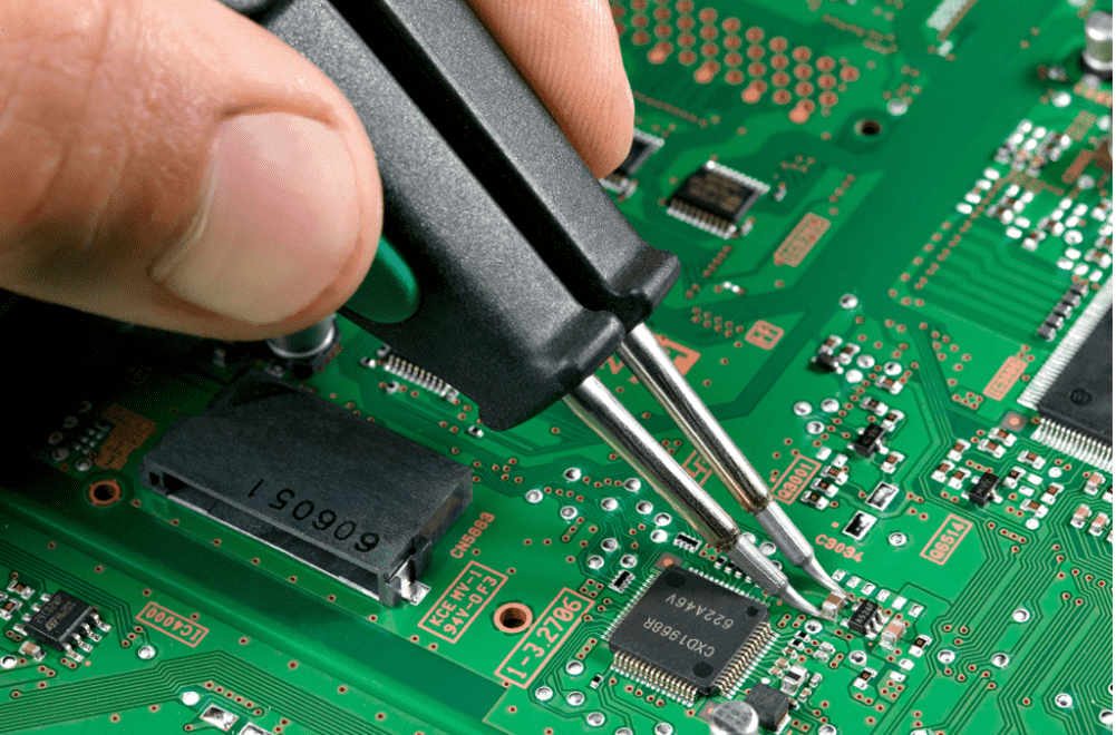
Tombstoning occurs when one end of a small two-terminal component lifts during the reflow process. Pad design, paste volume imbalance, uneven wetting, asymmetrical heating, copper thickness differences, and offset positioning during placement can contribute to the phenomenon. Although AOI may detect the position at the final inspection, the root-cause analysis for tombstoning generally requires associated SPI results, review of the footprint, and thermal evidence. Component rotation or lateral movement can be attributed to the same factors.
Tombstoning does not simply indicate a high-temperature issue. Typically, it reflects an imbalance in the wetting force or thermal response of each termination. A PCB assembler may be able to adjust the oven setting to correct this issue; however, using this approach alone may mask an imbalance in pad design, copper distribution, solderability, or paste transfer without correcting it.
Bridges, Opens, and Insufficient Joints
Solder bridging, open joints, and insufficient joints can result from many different sources: excessive paste, aperture design, size, spacing, incorrect placement, poor coplanarity of the component, and interactions during reflow operations. Open and insufficient joints may be the result of factors such as contamination of the solder paste or PCB, damaged or contaminated contact surfaces, inadequate wetting, insufficient heat, or other issues. Electrical tests can detect open and short circuits but will not always reveal the physical cause of these conditions without performing inspections and gathering additional process data.
For example, in the case of an open joint, it may not necessarily mean there was not enough solder paste applied. An open joint could have been caused by warping of the package or PCB, lead coplanarity issues, head-in-pillow behavior, oxidized surfaces, contamination of the PCB, or differences in the thermal response of the package and PCB.
Hidden Joints, Voiding, and Polarity Errors
Using optical inspection methods, BGA balls, QFN terminations, and exposed thermal-pad solder joints may not be viewable because they are hidden beneath the package when viewed from above. The use of X-ray inspection will allow the evaluation of joint alignment, bridging, opens, and void patterns; however, X-ray inspection alone cannot determine whether electrical connectivity or acceptable thermal performance exists for the joint.
Incorrectly assembled components, such as a wrong part, reversed polarity, or incorrect rotation, may have originated from errors related to the component’s BOM, feeder setup, centroid file, package markings, or machine programming. The assembly can be evaluated through a combination of FAI, AOI, electrical tests, and functional performance tests.
Context is also critical for understanding voids because determining failure or non-failure will depend on the type of application and the context of the void, such as its location, distribution, current path, thermal path, package guidance, and the approved acceptance requirement for voiding.
SMT vs. Through-Hole Assembly
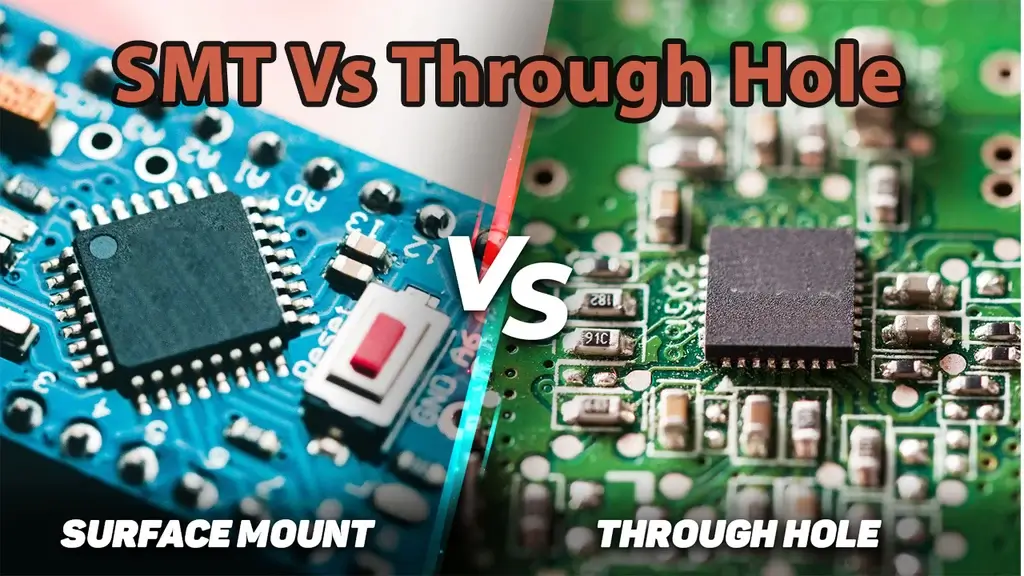
While SMT supports smaller formats and more efficient manufacturing processes, through-hole components are typically selected because of package availability or because their leads pass through plated holes and can support mechanical loads, creepage requirements, heat dissipation, current-carrying capability, and solder access.
However, the description of mounting methods will not provide an absolute measurement of mechanical strength or current-carrying capability. The mechanical performance of through-hole assemblies is dependent on the lead cross-section, the size and design of the hole and barrel, the amount of solder used to fill the barrel, the size of the copper connection, the degree of temperature rise above the ambient air around the assembly, and the amount of support.
SMT handles power differently from through-hole technology; therefore, power-handling capability will depend on the package design, pad size, copper-spreading capability, whether exposed pads or thermal vias are used, and the extent of cooling provided externally.
A surface-mount connector can use shell stakes or mounting tabs to support cable and connector loads when the connector is installed on the PCB, and additional anchors may be used for the same reasons as well. With a plated through-hole connector, the connector can transfer insertion forces through the PCB, and the hole pattern, clearance, and solder fill must be controlled. The best connector to use is dependent on the load placed on the signal contact during insertion, as well as the amount of flexing of the PCB before installation. The level of vibration present in a system, current requirements, and the intended repair method will also affect the selection of the connector type. If the enclosure will support the connector, the connector is also selected based on the expected usage and lifetime of the product, and not simply because it is available in a surface-mounted version.
Some connectors may be manufactured so that one housing can have a combination of surface-mounted signal contacts and through-hole tabs or shell stakes. Different connection methods may be used for electrical contacts and load-bearing features of the same connector.
The use of mixed assembly is common rather than contradictory, with one assembled PCB using surface-mounted components, such as passives, active ICs, and sensors, in addition to selected through-hole components, such as connectors, transformers, relays, and magnetic components.
Surface-Mount Examples That Depend on Package and Project
Different types of terminations are available for each package style, with various access and mounting methods. As such, different footprints, paste designs, placement techniques, reflow behavior, inspection methods, and repair needs should also be adjusted for each package type depending on the final assembly requirements.
Each package family has a different dominant risk. Chip passives depend on balanced pads, paste, and heating; SOIC and QFP packages add lead coplanarity and bridging; BGA packages add warpage and hidden-joint interpretation; QFN and DFN packages add exposed-pad paste segmentation, voiding, and side-joint visibility; connectors and power packages add board flex, mechanical loading, and heat removal.
The phrase types of SMT can refer to different classifications. A board may be single-sided, double-sided, or mixed with through-hole parts. A process may use reflow or another qualified attachment method. Chip, QFP, QFN, BGA, and connector examples are package families, not formal SMT process types.
Where Is SMT Used?
Compact Consumer and Wearable Electronics
Smartphones, wearables, compact sensors, and portable devices often use small passives, QFN, BGA, and double-sided placement to fit more functions into limited board area and height. The density creates tradeoffs among antenna keep-outs, battery placement, connector space, thermal concentration, inspection, and repair access. SMT enables the compact assembly; it does not by itself make the product faster, cooler, or more energy efficient. Dense consumer layouts may also place antennas, batteries, shields, flex connectors, and heat sources close to the same board area. Double-sided SMT can solve placement density while creating enclosure-clearance, shielding, inspection, and repair constraints that must be resolved at product level.

Automotive and Industrial Control
Logic devices, sensors, drivers, and small passives commonly use SMT in automotive and industrial controllers. Connectors, relays, transformers, or components exposed to mechanical load may use through-hole attachment or additional anchors. Vibration, thermal cycling, contamination, coating, connector loads, and the mixed-assembly sequence influence the design. Thermal cycling and vibration act through material-expansion differences among the package, solder joint, and PCB rather than through the industry label itself. Coating can improve environmental protection but may affect test points, connector contacts, heat transfer, and repair, so it must be considered with the assembly sequence.
Medical and Measurement Equipment
Medical devices and measuring devices typically benefit from the use of small SMD packages. The speed of production is not the only reason to consider compact SMD packaging. The compatibility of materials, residue control, cleanability, cleanliness evidence, traceability, orientation, inspection coverage, and electrical and functional verification could be far more important than the speed of production for a particular product.
Reliability claims related to SMT cannot be based on an assurance of zero failure. Rather, all reliability statements must include specific acceptance evidence and operating conditions associated with the actual functionality, operating environment, and specific method of acceptance.
For example, the term medical device does not refer to a single SMT process; the requirements for a wearable monitor, diagnostic instrument, and laboratory analyzer could be vastly different with regard to cleanliness, operating life, testing, and traceability.
RF and Communication Boards
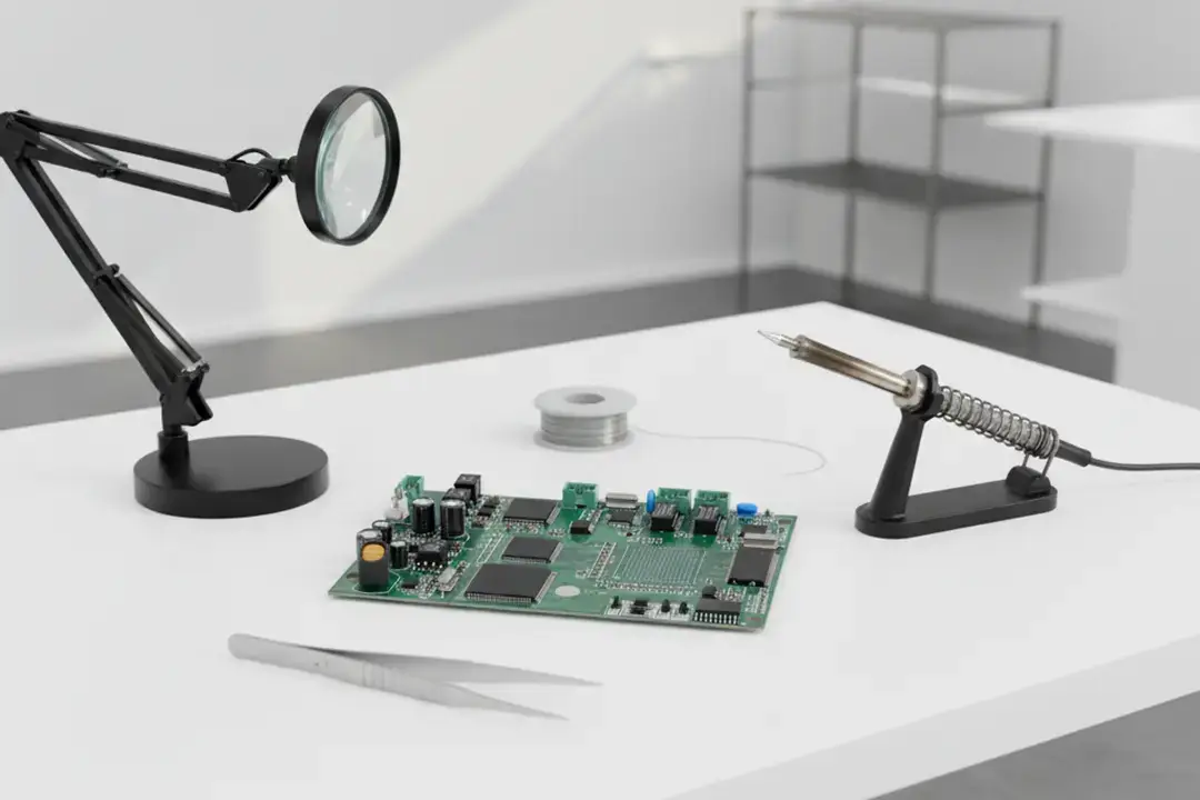
Short terminations and compact SMD packages can minimize parasitic effects and loop area in RF and communication circuits. As with all PCB assembly designs, the overall final performance will be determined by the PCB stackup, return path, ground transitions, impedance control, routing, and shielding, along with the package model and connector launch. While SMT provides the ability to produce a high-frequency layout, it cannot be substituted for electromagnetic design and measurement. Package and PCB transitions should be considered as one electromagnetic structure. Although short leads will provide advantages, a poor return path, via stub, ground discontinuity, connector launch, or shielding transition can offset those advantages.
LED and Power-Control Assemblies
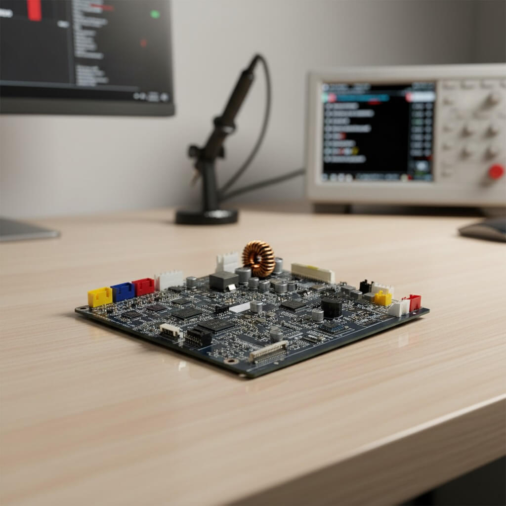
SMT components, such as LEDs, driver ICs, MOSFETs, rectifiers, and surface-mount power packages, are used in circuits that require substantial current and heat management. Both the design and assembly methods should be reviewed together, including exposed pads, copper areas, thermal vias, voiding, contact between the board and housing, and temperature verification. An example of a surface-mount power package specifically designed for high-current, thermally demanding applications is the Infineon DirectFET family.
Large magnetic components, connectors requiring high insertion forces, or creepage requirements may make through-hole attachment the most effective method. The rated power of an assembly does not determine whether SMT or through-hole attachment is appropriate for that component. For example, heat from an SMT LED or power package can leave through the leads, exposed pad, copper planes, thermal vias, and housing interface, while X-ray inspection provides evidence of the internal structure but not the operating temperature. Therefore, electrical load and assembled thermal conditions must be verified in conjunction with one another before the assembly is accepted.
Conclusion
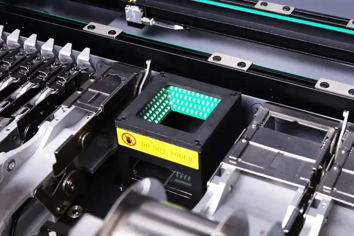
In conclusion, SMT is the technology used to mount components; SMDs are the devices, and PCBAs are assembled PCBs. A typical SMT process is based on the four basic steps of solder-paste printing, placement, reflow, and inspection and testing, but the exact materials, processes, and controls used are specific to the package and product types. The selection of SMT, through-hole, or mixed assembly will depend on the electrical, thermal, mechanical, inspection, and repair requirements and therefore should be evaluated individually rather than ranked globally.
References & Sources
- AN10365: Surface mount reflow soldering, Rev. 9, March 26, 2025 — NXP Semiconductors / Nexperia
- IPC-7525C: Stencil Design Guidelines, November 2021 — IPC
- IPC Releases “J” Revisions to Two Leading Standards for Electronics Assembly, April 8, 2024 — IPC
- Surface Mount Technology — an overview — ScienceDirect Topics
- DirectFET surface-mount power package technology — Infineon Technologies
- QFN and SON PCB Attachment, Rev. C, December 2023 — Texas Instruments