
Upload BOM & Gerber

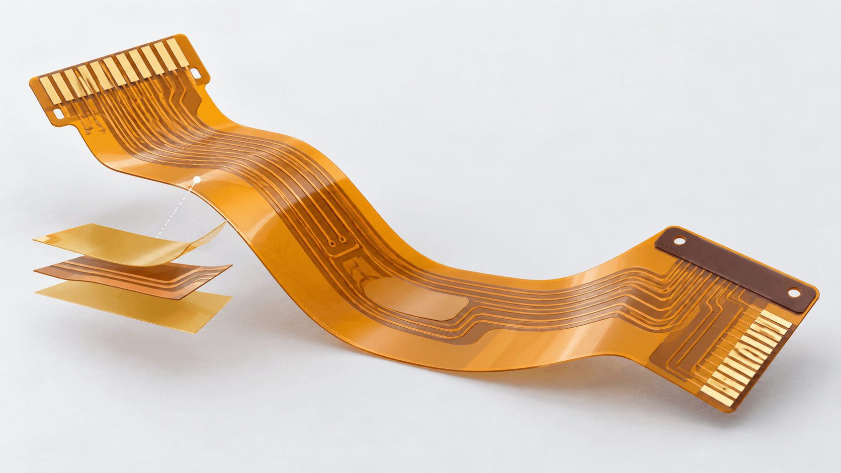
An FPCB is made from flexible substrates that are covered with copper. The finished FPCB is a patterned, interconnected, protected, finished, and tested bare circuit. The major difference between an FPCB and a rigid PCB is the bending capability of the dielectric construction used in the flexible circuit. Once the FPCB has been built, it can flex, conform, or move in several directions as required by the design of the product in which it is used. Therefore, an FPCB is used when it is necessary to route a connection through a hinge, a small enclosure, or another type of moving assembly, as opposed to routing it through a flat board area.
For fabrication ranges, materials, fine-line limits, controlled impedance, and dynamic-flex capability, see SUGA's flexible PCB manufacturing capabilities.
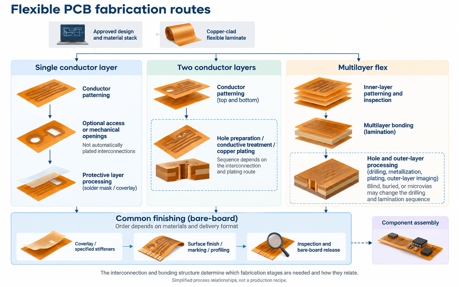
Some interconnection operations can be omitted from single-sided flexible circuits, while multilayer flexible circuits may require those operations. In addition, this same route can be used when multiple steps are repeated or reordered for multilayer, blind-via, buried-via, or sequentially laminated flexible circuits.
Contents
show
14-Step Flexible PCB Manufacturing Process
STEP 01 — DFM and CAM Preparation
Fabrication starts only after the DFM has been confirmed and the released conductor data, drill data, material construction, mechanical definition, and acceptance requirements describe the same circuit revision. The DFM checks ensure that the FPCB as designed matches its intended fabrication, while CAM converts the released design into imaging, drilling, routing, tooling, and inspection data.
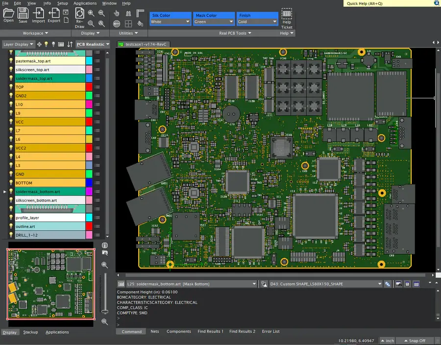
In addition, design-rule checks inside PCB software are limited to the rules programmed into the software and do not cover the manufacturing process by themselves. All other aspects of manufacturing, including material handling, panel design, local dimensions, bend regions, coverlay openings, stiffener placement, and inspection states, must also be considered during PCB preparation.
Controlled impedance or shielding must also be associated with the entire mechanical stack, rather than solely defined by trace width. The addition of shield layers, adhesives, and cover materials changes local thicknesses, thereby altering both the electrical and mechanical characteristics.
STEP 02 — FCCL Material Preparation
FCCL is the base material and is normally manufactured using polyimide for higher-temperature flex circuits or polyester for lower-temperature flex circuits. The laminate manufacturer will combine the copper and dielectric materials, and then the PCB fabricator will cut, panel, pattern, interconnect, protect, and finish the laminate.
Material selection is one of the many process variables that will impact the construction of the final product. With dielectric thickness, copper thickness, copper type, and adhesive system being part of the starting material selection process, they all affect the final product; this includes the handling and etching processes, the finished thickness after lamination, and how the circuit responds to bending. The table uses published all-polyimide FCCL construction data as one material-family example rather than an industry-wide limit.
The dielectric thickness will establish part of the starting thickness used to create the flexible circuit and will therefore affect handling stiffness, dimensional movement, and bend ratio. Increasing copper thickness results in an increase in conductor mass and mechanical stiffness; thus, the copper thickness affects the etching load on the circuit. Copper foil type will affect the mechanical performance of the base foil. The adhesive system will also impact the thickness of the completed stack-up, as well as the way in which the adhesive interfaces with the laminates and how much polymer material is contained within the flexible area of the stack-up.
The design guidance for flexible circuits focuses on the ability of an adhesiveless substrate to reduce starting thickness compared with an adhesive-based substrate. This reduction typically ranges from approximately 0.001 to 0.002 inches (25 to 51 µm) for each layer of material compared with an adhesive-based substrate. This reduction in thickness increases the bend ratio and subsequently increases the mechanical margin of the flexible circuit when bent at a fixed radius.
When defining the mechanical context of a bend ratio, it can be defined as the radius of the bend divided by the final thickness of the flexible circuit. 6x the thickness for single-layer flex circuits and 12x or 24x for double-layer and multilayer flex-circuit designs are the planning minima according to the published design guidelines for flex circuits; however, separate assessments will be necessary for repeated-motion applications rather than using the same ratio as for other flex-circuit designs.
For example, at a finished thickness of 0.20 mm, a 12x bend ratio correlates to a bend radius of 2.4 mm, while a 24x bend ratio correlates to a bend radius of 4.8 mm. If the radius remains the same at 2.4 mm and the finished thickness changes from 0.10 to 0.20 mm, then the bend ratio would decrease from 24x to 12x. Therefore, plating, adhesive, coverlay, or reinforcement in the bend area will create a tighter mechanical condition, even though the circuit outline remains unchanged.
STEP 03 — Surface Cleaning and Resist Preparation
Before the photoresist pattern is applied, copper surfaces should be cleaned and conditioned, as oils, oxides, particles, and handling residue will negatively affect the adhesion of the photoresist and hinder the transfer of the image. A thin gauge of flexible material also needs to be properly supported during cleaning and wet processing, as wrinkling or movement of the panel can disrupt proper registration.
The quality of surface preparation directly impacts the adhesion of the photoresist, which in turn affects the integrity of the protection applied to the copper and determines which copper will remain following the etching process. A defect introduced during surface preparation can produce pinholes, incomplete etching, unwanted copper, or damaged conductor edges.
Material direction, panel reference features, and dimensional changes that occur after exposure to moisture or heat also play an important role in registration. Process compensation must take these factors into account to align with the material and its process history, rather than simply using a standard shrinkage figure for a laminate.
STEP 04 — Circuit Imaging and Developing
The imaging process produces a pattern on the resist, and the development process removes the intended resist areas to expose copper for the next operation. The alignment, exposure, and development processes together determine the geometry of the resist that will ultimately indicate the widths of traces, spacing between traces, shape of pads, and registration.
- If the development process is incomplete, resist may remain where copper is intended to be removed, providing an opportunity for unwanted copper or bridges to remain after etching.
- If the development process is excessive, the pads or edges of the conductors may be exposed to etchants, and the protection of the conductors by the resist will be diminished during etching.
- A misalignment of the circuit boards may cause the pads, openings, or conductor features to be misaligned although the electrical image may appear correct.
STEP 05 — Copper Etching and Resist Stripping
Etching is the process used to remove the exposed copper, while the resist protects the intended conductors. After the resist has served its function, it is removed from the surface of the circuit. An alkaline resist stripper and a copper etchant perform different functions, so the chemistry and process control for one cannot be substituted for the other.
The amount of copper entering the etching tanks is not always equal to the thickness of the original copper foil. If earlier processing deposited copper over a larger area, the etching process must also remove that additional copper. The plating strategy of the circuit therefore affects the ability to create fine-featured conductors and the geometry of the conductors.
If the thickness of the starting or deposited copper is greater, then a greater amount of copper will be required to etch and therefore, lateral etch control will need to be more stringent. The width, spacing, pad shape, and edge condition of a conductor will therefore require tighter verification. Published flex fabrication guidelines show trends in the use of 3/3 mil line/space with 1/3 oz copper, 4/4 mil with 1/2 oz copper, 5/5 mil with 1 oz copper, and 7/7 mil with 2 oz copper. Although these examples are process specific and not industry or standard limits, they do illustrate that increasing copper thickness will result in larger line/space minimums being used.
Bridges or reduced spacing can result from residual resist, while loss of resist protection can create thinner conductors, notches, or openings. Unsupported flex will also have an increased probability of registration shifts, wrinkles, or dimensional defects.
As a result, a single published minimum line/space value does not adequately define every flex process. Practical feature envelopes will be influenced by copper thickness, plating order, resist systems, etchant controls, and the way that the printed circuit is handled.
STEP 06 — Inner-Layer Inspection and Multilayer Lamination
Single-sided flex does not utilize multilayer bonding, while multilayer flex does, as inner conductors must be patterned and inspected before being covered. After layers are laminated, a final inspection of the individual inner conductor patterns is not possible, as there is no longer an unobstructed view of those patterns.
During lamination, patterned flex layers are mated to the dielectric or bonding materials of choice; the temperature, pressure, and dwell cycle used is material specific. Registration, dimensional movement, adhesive flow, air removal, and surface condition all affect the positioning of the interlayer in the completed assembly and the quality of the bonds between those layers.
Blind, buried, or sequential interconnect structures may necessitate repeat cycles of imaging, laminating, drilling, or plating of specific parts. As a result, the manufacturing traveler should mirror the actual stack and via structure.
STEP 07 — Drilling and Hole-Wall Preparation
Non-plated holes are for clearance, tooling, or mechanical purposes, while plated through-holes connect specified conductive layers. When drilling an electrical hole, the hole geometry is formed by drilling, while hole-wall preparation cleans and conditions the insulating wall before conductive treatment and copper deposition.
When calculating the aspect ratio of a hole, the ratio of hole depth to hole diameter must be calculated. The aspect ratio of a hole has an impact on access for desmear or cleaning, conductive treatment, copper distribution, and post-production inspection.
At the same stack thickness, as the diameter of the hole decreases, the aspect ratio increases. Conversely, as the diameter of the hole remains constant, increasing the thickness of the stack creates additional challenges with uniform wall preparation and copper deposition. A published flex manufacturing capability uses 10:1 as a maximum plated-through-hole aspect ratio. For example, a hole depth of 1.0 mm with a finished diameter of 0.10 mm has an aspect ratio of 10:1; but should the hole depth increase to 1.2 mm with the same finished diameter, the aspect ratio would be 12:1 and would be beyond that published process capability. This is a capability benchmark rather than a universal industry limit. The use of blind, buried, or microvia structures may require the repetition of drilling, conductive treatment, plating, and lamination cycles; holes located in moving bend regions will also require consideration of cyclic tension and compression.
An unbroken electrical path requires a suitable hole structure and continuous deposited copper throughout the hole barrel. Cross-section or other structural inspection provides a more detailed picture of the physical hole wall.
STEP 08 — Copper Plating
After the hole wall is made conductive, copper deposition forms the electrical connection between specified layers and can also increase conductor thickness.
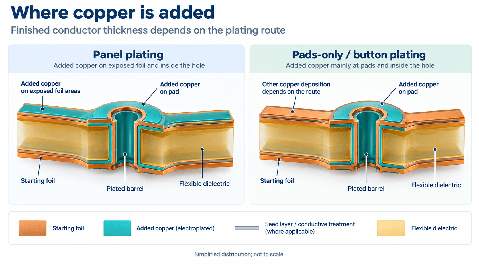
The process of panel plating has a shorter processing route and can increase current-carrying copper throughout the circuit. However, the added copper must be etched away later in the production process and also creates added rigidity in the moving flex zone. On the other hand, pad-only plating requires more operations but keeps most conductor regions closer to the thickness of the base foil so that finer-feature etching can be accomplished more easily while preserving more flexibility in the bending zone.
The base foil type and deposited copper represent distinct material states. Rolled-annealed base foils are commonly considered preferable where repeated flexing is important, while electroplated copper introduced during manufacturing can decrease flexibility when it extends into the moving flex zone.
STEP 09 — Coverlay Alignment and Lamination
The purpose of a film coverlay is to protect the conductors while allowing pads, contacts, and certain openings to remain accessible. The fabricator is responsible for forming the openings, aligning, tacking, and laminating the film under the process conditions required by the material system.
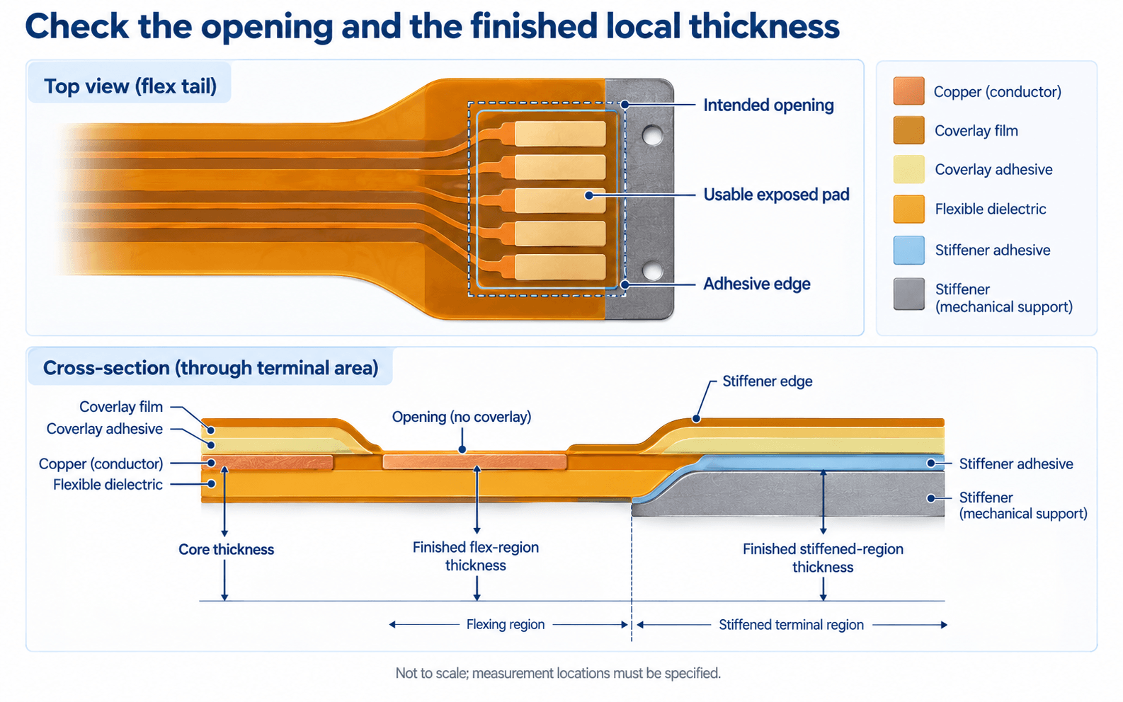
Process data published for acrylic-polyimide coverlay processing, including the parameters of temperature, pressure, and dwell time, are provided below. The adhesive-flow value is derived from data for related adhesive sheets. These examples are material-specific and should not be considered universal settings for every coverlay or adhesive system.
Adhesive characteristics, including softening, wetting, and cure, are controlled by temperature; pressure forces intimate contact and influences adhesive movement over the copper features; dwell time is necessary for bonding. The related sheet adhesive has a specified example flow of 0.05-0.10 mm; therefore, the nominal cut opening cannot be regarded as the actual post-lamination opening. Excessive flow can reduce usable pad exposure; if air remains trapped or bonding is insufficient, voids or separation can occur. Therefore, moving outside a material-specific process window should be validated rather than assumed to produce the same opening geometry and bond condition.
Coverlays, bondplys, core adhesives, and stiffener adhesives perform different functions even when they use related polymer systems. Their thicknesses contribute to the overall finished flex stack thickness, so thermal processing and final mechanical thickness remain linked.
STEP 10 — Stiffener Bonding
A stiffener serves as an additional point of support within a connector finger area, termination area, component zone, or other location requiring controlled rigidity. However, the relevant dimension is not simply the thickness of the stiffener; rather, the stiffener must be evaluated in conjunction with the thickness of the flexible circuit and the adhesive layer with which it bonds.
Mating thickness can be defined using the following relationship: finished flex thickness + stiffener adhesive + stiffener material. Depending on where the thickness is measured, connector compatibility, insertion depth, contact pressure, and the transition into the bend region all depend on the local mating thickness. The total thickness at the connector, when adding a flexible circuit measuring 0.10 mm to an adhesive that is 0.05 mm thick and an FR4 stiffener that is 0.20 mm thick, results in a local mating thickness of 0.35 mm. If the stiffener thickness alone is increased to 0.30 mm, the local mating thickness increases from 0.35 mm to 0.45 mm. Connector datasheets specify a tolerance window for mating thickness, and a change of this size can move connector contact pressure or insertion force outside the qualified range even though the flexible circuit and adhesive have not changed.
The edge of a stiffener changes the local bending boundary at the transition into the flexible circuit. Keeping repetitive motion away from these transitions and measuring the finished mating region after bonding will provide greater control over performance than depending solely on nominal material thicknesses.
STEP 11 — Surface Finishing
Surface finishing is the treatment of exposed pads or contacts that will be used for soldering, making electrical contact, wire bonding, or preventing oxidation. ENIG, ENEPIG, hard gold, immersion silver, immersion tin, OSP, and other types of finish serve different functions at the interface; the drawing and intended use will define how each exposed area is treated.
Surface finishing is separate from the copper that is used to plate a hole wall and the coverlay used to insulate a conductor. Mixing functions may reduce the clarity of their purposes in the following ways: hole copper provides interlayer continuity; coverlay protects the covered circuitry; finish modifies only the designated exposed interface.
The means through which quality control verifies finish coverage and exposed geometry at the actual contact area are different from those used to verify dimensional and electrical characteristics of a product. The specification for the finish alone does not define registration of the coverlay, plated-hole structure, or bending performance.
STEP 12 — Profiling and Marking
Final profiling creates the circuit outline as an independent entity from the manufacturing panel or can provide a delivery array while retaining necessary support features. Due to differences in tooling, edge condition, geometric freedom, tolerance behavior, and suitability for production quantity, laser cutting, routing or milling, and die-based methods have different applications in profiling.
The profiling method selected should depend on the geometry, tolerance, and production quantity required for the product. Low-volume or tight internal feature geometries can benefit from programmable cutting options, while production runs can justify dedicated tooling where the required edge and dimensional performance are compatible. Edge condition is also a variable associated with flex reliability; any burrs, nicks, or rough transitions located near a bend zone can increase stress concentration and act as a point of initiation for tearing during repeated flexing motion.
Markings can provide a means of identifying a part, controlling revisions, tracking lots, or tracing an item by serial number. Marking cure time, adhesive cure time, moisture conditioning, and profiling are separate operations; thus, their sequence can vary based on the material system and delivery format utilized.
STEP 13 — Inspection and Electrical Testing
Quality control activities are dispersed throughout the production process rather than being solely conducted upon completion of production. Internal pattern checks are completed prior to bonding, plated-hole structures are checked after interconnection processing, registration of coverlay is confirmed after lamination, dimensions are checked post-profiling, and final electrical continuity and isolation are verified against the approved definition of connections.

Electrical verification is clearly separated from the physical characteristics of circuits, including conductor geometry and feature registration, per IPC-9252B. A passing electrical test only indicates that the tested network successfully passed the defined continuity and isolation parameters; it does not confirm every structural, dimensional, mechanical, or service requirement of the product. Typically, a test program will cover 100% of all nets for continuity and isolation, while intermediate points along each net may be optimized out. Electrical isolation resistance thresholds that denote a “short” will differ according to class and test level; therefore, a passing result confirms that resistance remained above the threshold used by the test program, not the complete absence of leakage at every point along the net.
AOI and dimensional checks cannot demonstrate every hidden electrical connection; an electrical test cannot confirm plated-hole geometry, assembled function, or bending life; each destructive cross-section provides evidence of the sampled structure only and not every delivered circuit; and appearance alone does not prove the overall quality of internal bonds.
For repeated bend testing, maintain an accurate record of the specimen’s construction, finished thickness, bend radius, travel, cycle count, environment, and failure criterion. A foil type or a passing continuity test cannot be turned into a universal service-life number without including those essential variables.
IPC-2223F provides guidelines for flex and rigid-flex design; IPC-6013F addresses qualification and performance of flexible and rigid-flex printed boards; and IPC-9252B provides guidance for electrical testing of unpopulated boards. Each of these documents answers different questions and cannot be substituted for one another.
STEP 14 — Packing and Delivery
Packing and shipping materials protect the finished bare circuit boards from being accidentally folded, contaminated, scratched, or affected by uncontrolled moisture during storage and transport. The condition of the circuit upon delivery must retain the approved revision, individual-circuit or array format, stiffeners, openings, protective support, and traceability markings.
Raw-material storage instructions do not automatically define the finished-board packing method. Vacuum packaging does not determine whether the bare boards require moisture-removal preparation prior to assembly. The determination of preparation is based on the final construction, exposure history, destination process, and handling method.
This point is the formal end of the bare-board fabrication process; all activities associated with paste printing, component placement, soldering, and assembly acceptance are part of flexible PCB assembly rather than the 14-step bare-board manufacturing route described above.
How the 14 Steps Work as One Manufacturing System
Across the 14 control points, the same variables recur: material thickness affects wet-process handling and bend ratio; plating affects both etch load and bend-region stiffness; lamination affects opening geometry and local thickness; and final inspection confirms only the properties measured by the inspection method used. Keeping these relationships explicit helps separate circuits that can be fabricated from those whose construction and quality requirements have actually been verified.
References & Sources
- Flex Solutions Design Guide – Minco
- Pyralux AP All-Polyimide Double-Sided Copper-Clad Laminate – DuPont
- Flex Circuits – Minco
- FPC TECH GUIDE – Molex
- IPC-6013F – IPC
- Printed Circuit Board – Chemcut
- Photoresist Developers – Chemcut
- Photoresist Stripping – Chemcut
- Advantages of Pads Only & Panel Plating Techniques – Minco
- Designing a Flex Circuit for Flexibility – Minco
- Pyralux LF Acrylic-Based Coverlay – DuPont
- Flex & Rigid-Flex Manufacturing Process – Epec
- IPC-9252B – IPC
- IPC-2223F – IPC
- Flex Circuit Polyimide Coverlay & Solder Mask Considerations – Epec


