Upload BOM & Gerber

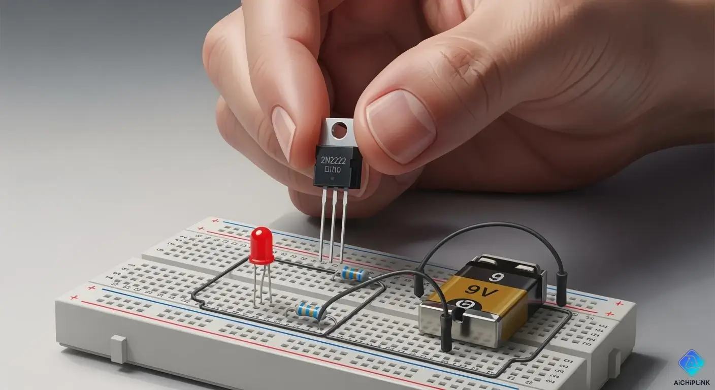
There is no standard family-wide pinout for 2N2222 components. Before determining the functions of the pins (emitter, base, collector), you must identify all information regarding the specific part number, manufacturer, package type, and view via the datasheet. Use the diode test method while powered off only as an additional cross-check, not to assign the leads by itself. You must also verify that the schematic pin numbers correspond to the footprint pads and the BOM package assignment before wiring or assembling.
Because there is no universal pinout for bare 2N2222 components, it is impossible to assign specific functions to the three leads from the part name alone. The 2N2222 family is manufactured in various forms (metal-can, plastic through-hole, surface mount), whose manufacturers may use differing lead maps based on the specific part number, manufacturer, and case style. You should qualify each pinout by its original manufacturer, specific part number, specific case style, and location referenced in the illustration to determine how to identify each lead's function.
An incorrectly copied unrelated pinout diagram or mirrored valid pinout diagram will switch the emitter and collector leads and propagate an error into the schematic symbol, PCB footprint, BOM, and placement drawing.
Contents
show
What Is the 2N2222 Pinout?
The correct pinout for a 2N2222 component can only be determined by taking into consideration the emitter, base, and collector configuration used by the manufacturer for a particular part number, case style, and manufacturer's illustrated view. A 2N2222 component is an NPN bipolar transistor; however, the definition of NPN only defines the functionality of the leads (emitter, base, collector), not the location of the leads on the manufacturer's physical case.
The bias and load determine whether a BJT behaves as a switch or a linear amplifier. In either case, the terminals must be correctly assigned as base, collector, and emitter (B, C, and E). In addition to the terminal assignment, an issue that arises when reading the BJT's part number (e.g., 2N2222, MMBT, PN) is that the corresponding physical pin locations may not match a generic pinout diagram or the selected PCB footprint.
In contrast to assigning pins based only on the terminal letters, the correct way to connect a BJT is by using the manufacturer's mechanical drawing as a reference. If a manufacturer provides a source with enough detail (vendor name, complete marking, housing, and viewing direction), the source can be used for pin assignment.
Why Can the Same 2N2222 Name Show Different Pinouts?
Lead map validity will differ from one supplier to the next due to the supplier's complete ordering code, body style, and mechanical-drawing convention for their 2N2222 families. A name alone does not imply a universal standard for a housing. Instead, prefixes such as P2N or PN and suffixes such as A can help scope the search without replacing the primary documents for that component.
When creating the BOM or Library Note, record the Pin Map together with the orientation shown in the manufacturer drawing. If you cannot determine the orientation of a schematic drawing, refer to the original datasheet to confirm the pin map orientation.
2N2222 vs 2N2222A, PN2222A, and P2N2222A
When comparing multiple part numbers, 2N2222, 2N2222A, PN2222A, and P2N2222A, "A" does not imply a plastic package. Microchip lists a 2N2222A in a TO-18; however, related documentation includes a surface-mount 2N2222AUB on the Microchip 2N2222A product page. Likewise, PN2222A and P2N2222A are different from one another by more than one character; the supplier drawings for PN2222A and P2N2222A have TO-92 lead orders in opposite arrangements, as indicated in the Exact-Device Table above. When comparing these different part numbers, these are related device designators and do not represent interchangeable pinout codes. To ensure electrical suitability and to perform proper physical mapping, a part may electrically meet the requirements of a circuit (voltage & current), yet have a different lead configuration, package type, or land pattern.
If an orderable part number appears, verify the part number, current lifecycle, and package documentation for a new BOM; do not substitute from an equivalent list.
When producing a diagram for your PCB, refrain from reducing it down to the designation of "Flat Side Facing Me" or "Left to Right." Such representations fail to capture case style and viewing direction. Always maintain the orientation of your schematic with respect to each of the pin maps you create.
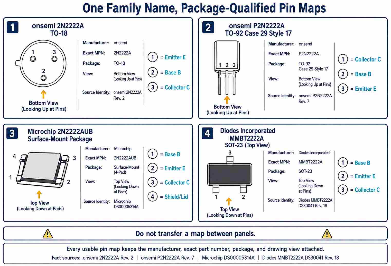
Match the Exact Part, Package, and Drawing View
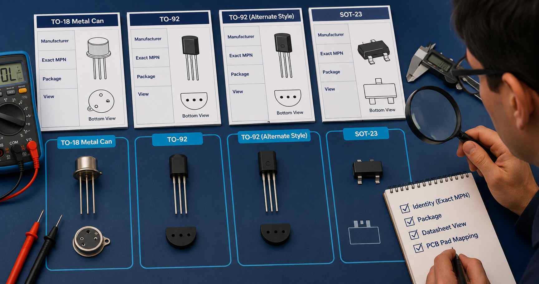
To establish a complete pin map comparison, each of the following fields must match: complete marking, manufacturer, package, and datasheet view. Once any of the above four fields does not match, the mapping will be incomplete. Just connecting power to a circuit and checking to see if the circuit functions does not definitively prove which pin has which function. It simply shows whether the circuit is functioning under its current configuration.
- Record all markings on devices, including every evident prefix and suffix (e.g., do not record just "2222" or "2N2222").
- Classify the enclosure types that the device is housed in (e.g., metal TO-18, leaded TO-92, SOT-23, and other styles used for surface-mount).
- Locate the manufacturer's documentation for the device. Check the manufacturer's logo, ordering code(s), housing options, and revisions.
- Examine the perspective from which the labeling was made. Determine whether the figure represents a top view, a bottom view, a lead view, or a numbered-package view.
- Write an accurate description of your observation. Describe the vendor, the MPN, the enclosure type, the orientation of the part in the enclosure, and where each lead is located in numerical order.
For example, onsemi P2N2222A, TO-92 Case 29, Style 17; from the package document, lead 1=C; lead 2=B; lead 3=E. Write down the accurate mapping of the leads in a way that another person can review the results without relying upon memory.
Incomplete or faint markings lower the confidence level in identifying the part. You can refer back to your purchase history, the reel/bag label information, and the dimensions of the components. If you can't relate the device to the manufacturer's controlled documentation, mark it for noncritical identification work only and do not approve it for production placement.
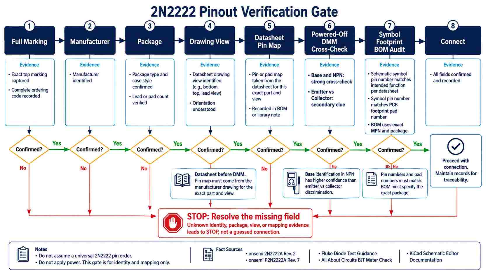
How Do You Verify a 2N2222 with a Multimeter?
- Disconnect power to the device before performing a multimeter diode test and discharge the capacitors. Isolate the BJT from the circuit by lifting one lead or extracting the device from the circuit if you have an ambiguous set of data (Fluke diode test).
- Label the unknown leads A, B, and C for your temporary test purposes. Measure all combinations of A, B, and C with both probe polarities.
- Identify the common node by connecting the red probe to it. The other two leads should show forward-junction readings from the common node. Following this pattern will provide a high level of confidence that you have identified the base lead in an NPN transistor.
- Reverse the probe polarity to the two junctions. Both junction connections should block, provided the meter range is appropriate and residual circuit paths do not affect the measurement.
- Compare the forward-connected readings as a secondary clue distinguishing between the collector and emitter leads. It is not uncommon for the readings to be close and inconsistent relative to the other measurements.
When you measure the above example of the BJT, you are determining how the two PN junctions relate to each other by virtue of the fact that they both share a common base. This method allows you to identify the common node in your measurements, but it will not allow you to make a final determination of which lead is the emitter and which is the collector. The method of using the forward drop as a comparison is only an additional clue, not a definitive method of establishing the relationship between the two leads (BJT meter tests).
If, upon measuring the BJT, you find conflicting information as to the identity of the device, look over the complete set of markings, review the manufacturer, housing, and device perspective, and look over any other sources available to you before making any wiring changes to the BJT.
Map Datasheet Pins to the Symbol, Footprint, and BOM
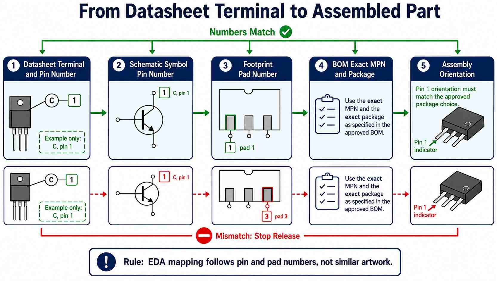
NPN symbols can connect to incorrect copper due to the way PCB tools match footprint pads to symbol pins using numbers. Using only the labels "E," "B," and "C" on the screen is not enough. You must trace each logical terminal back through the library and purchasing data before releasing the board.
- Use the terminal name and physical pin/pad number from the source document.
- Confirm that the schematic symbol has that number assigned to the appropriate function (E, B, or C).
- Check that the footprint will put it on the proper copper land in the documented orientation.
- Cross-reference the BOM with the specific manufacturer part number and ordering option.
- Compare the placement rotation, silkscreen, and assembly artwork against either an orientation mark or mechanical figure.
The official KiCad schematic documentation indicates that pins from symbols and pads from footprints are matched by number (KiCad Schematic Editor documentation). Altium, Eagle, and other EDA tools also use pin-to-pad mapping; you must check the specific rules of each EDA tool regarding pin-to-pad matching rather than assume the tool functions similarly to KiCad.
Which Ratings Matter Before You Use It as a Switch?
Before switching loads, you must review VCEO, collector current limits, power dissipation, temperature, VCE(sat), and drive conditions for each specific component before making any decisions regarding switching. The absolute maximum ratings are meant to be stress boundaries and are not the same as recommended operating points; do not merge numbers from non-identical housings into a single family specification.
As these conditions vary, these values should only be used to set "lookup" boundaries, not as a best-to-worst ranking.
The hFE parameter (also known as current gain) is defined by both the load on the collector and the applied test voltage. A single typical value should not be applied over the entire operating range. When using saturated switching circuits, compare the intended collector current with the manufacturer's VCE(sat) test conditions, then verify that the driver can safely supply sufficient base current.
The datasheet for a Diodes MMBT2222A says that the device was tested using 150 mA collector current and 15 mA base current in saturation and was then also tested using 500 mA collector current and 50 mA base current in saturation, with a forced beta of 10 for both tests. These ratios are a result of two test points and do not create a universal resistor rule for each circuit utilizing a 2N2222.
How Do You Use a 2N2222 as a Low-Side Switch?
For common low-side switch circuits, the load will connect between the upstream positive voltage source and the collector, while the emitter must return to ground. To drive the base, the controller should apply current through a current-limiting resistor to the transistor. The package pinout should map the correct schematic topology to physical leads for each electrical connection on the circuit board; however, even with the correct schematic topology, if the footprint on the circuit board uses the incorrect pad number for E, B, or C, the circuit will still fail on the circuit board.
To determine the base resistor value for driving a load at a specific current, use the base current at that collector current point from the datasheet rather than some arbitrary "typical" hFE derived from the summary line. The MMBT2222A datasheet specifies IB = 50 mA to achieve IC = 500 mA, using a forced beta of 10. If the 5 V driver can safely supply the required base current, calculate the base resistor as Rb = (VIN – VBE(sat)) / IB. Use the value for VBE(sat) obtained from the same electrical-characteristics table rather than the common small-signal value of 0.7 V; near saturation, VBE(sat) tends to run higher. At IC = 500 mA and IB = 50 mA, the datasheet lists VBE(sat) up to 2.0 V, so the 0.9–1.0 V estimate and 68 Ω or 75 Ω values should not be treated as guaranteed across operating variation.
When designing a circuit for a relay or motor load, include a flyback diode (a 1N4148- or 1N4001-class part rated above the coil's peak current) across the relay or motor coil, cathode to the supply rail, then verify the transistor ratings for continuous and pulsed current against both the startup/stall current and normal running current, as inrush current for a motor may be several times greater than the steady-state running current during the first tens of milliseconds.
When designing a circuit for a LED, the series resistor value can be determined using (VIN – VLED) / ILED. The transistor power dissipation at the selected collector current must remain below the package limit at the expected ambient temperature.
Can a 2N3904 or BC547 Replace a 2N2222?
The following qualification requirements should be met:
- Confirm the NPN lead configuration for the replacement compared to the original.
- Compare voltages (VCEO, VCBO, VEBO), continuous current rating, pulsed load rating, and power dissipation rating under the operating conditions.
- Confirm hFE for the intended collector current, not just the stated typical value.
- Confirm VCE(sat) for the intended input condition (base drive level available from the controller).
- If edge speeds are important, check the transition frequency or switching times of the replacement.
- Confirm footprint dimensions, lead spacing and orientation, thermal path, and purchasing status of the replacement.
The 2N3904 from onsemi has a continuous collector current rating of only 200 mA (onsemi 2N3904 datasheet), which is one-third the continuous collector rating of the P2N2222A (600 mA) and one-fourth the continuous collector rating of the 2N2222A (800 mA). This difference is significant enough to prevent the use of any rule of thumb regarding the substitution of three-lead NPN transistors and alone cannot qualify any lower-amperage application.
The BC547 must be qualified in the same way as a replacement transistor; it cannot simply be swapped for the original based on its name. In the onsemi TO-92 drawing, the BC547 is numbered 1=C, 2=B, 3=E, matching the onsemi P2N2222A's numbered lead order rather than reversing it. Substitution still requires the exact manufacturer package drawing and footprint to be checked. The BC547 has a VCEO of 45 volts and a continuous collector current rating of only 100 mA, which is roughly 1/6th of the continuous collector current rating of the P2N2222A and 1/8th the continuous collector current rating of the 2N2222A. The BC547 may be sufficient for small-signal switching applications and low-power amplification, but is insufficient for applications requiring the higher current-handling capability of either the P2N2222A or the 2N2222A. Although the MMBT2222A shares the same "2222" family designation, it may require a different SOT-23 footprint and assembly orientation than either the P2N2222A or the 2N2222A.
Diagnose a Reversed or Wrong-Footprint Transistor
To diagnose the pinout error, examine the symptoms of the transistor and follow the data chain rather than rotate the transistor and try again. Before doing any of this, be sure to disconnect the power supply and discharge any stored energy.
If you are testing an unknown, replace any transistors that have experienced significant stress before you consider a corrected reading to be confirmation of normal operation.
Verify the orientation for leaded devices as you assemble them into through-hole assemblies. In addition, maintain the pad map and orientation of MMBT2222A or other surface-mount types during assembly by preserving the pad rotation and pad map throughout SMT assembly. If the upstream library identifies the wrong terminal for a numbered pad, neither assembly method will correct that mismatch.
References & Sources
- 2N2222A NPN Silicon Transistor Datasheet Rev. 2 – onsemi
- P2N2222A Amplifier Transistors Datasheet Rev. 7 – onsemi
- PN2222A NPN General Purpose Amplifier Datasheet Rev. 1.1.0 – Fairchild Semiconductor
- 2N2222A Transistor Product Page – Microchip Technology
- 2N2222A Datasheet DS00005314A – Microchip Technology
- MMBT2222A NPN Small Signal Surface Mount Transistor Datasheet DS30041 Rev. 18 – Diodes Incorporated
- How to Test Diodes with a Digital Multimeter – Fluke
- Meter Check of a Transistor BJT – All About Circuits
- Schematic Editor Documentation – KiCad
- 2N3904 General Purpose Transistors Datasheet Rev. 3 – onsemi
- BC546/547/548 NPN General Purpose Transistors Datasheet – onsemi