Upload BOM & Gerber

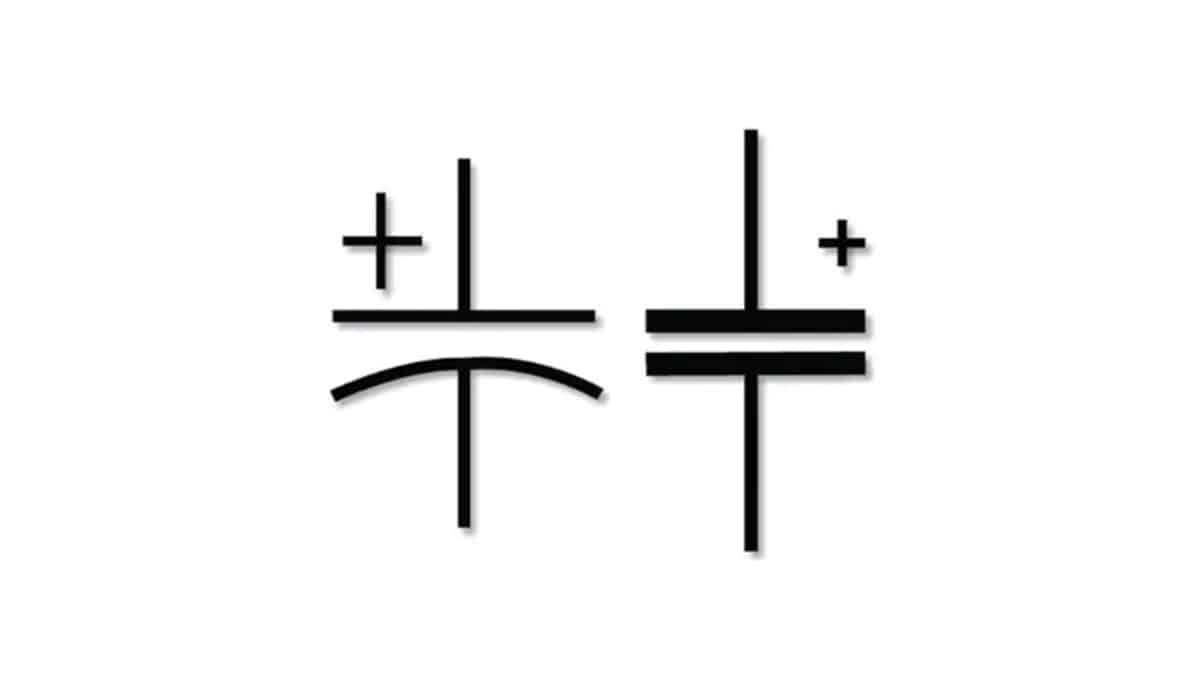
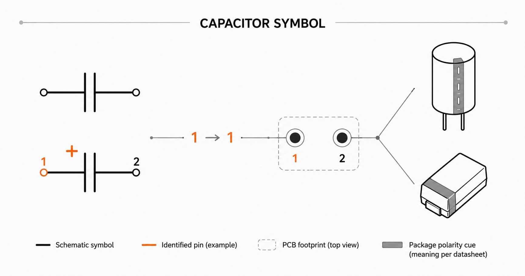
In a basic capacitor symbol, two conductive plates are represented with a gap between them, with one terminal to the left side of the symbol and another terminal to the right side of the symbol. This symbol indicates the electrical function of the capacitor and does not provide details regarding package shape, size, voltage rating, or printed markings, which can all be found in other locations.
For a polarized capacitor, a plus (+) mark may be visible on one side to indicate the location of one terminal in a schematic; however, it is still possible to produce incorrect assembly drawings if the library pins, footprint pads, and polarity markings on the physical part do not match.
Contents
show
What Does a Capacitor Symbol Show?
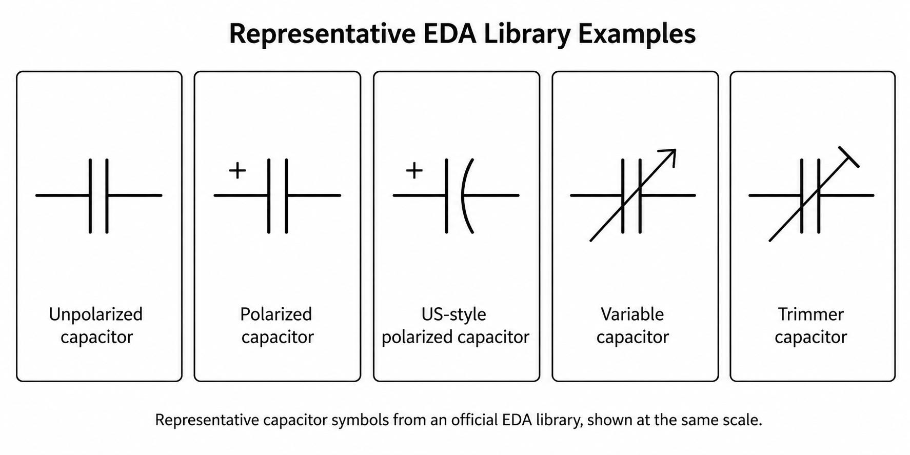
An example is the KiCad C capacitor symbol that has two straight plates, uses the reference prefix of "C," and is identified as "Unpolarized capacitor" in the KiCad library file.
Each symbol, reference number, and value provides unique information. In the case of "C1 10 µF", "C1" is the unique identifier for a single capacitor component instance in the schematic; "10 µF" is the value of the capacitor.
Common Capacitor Symbol Families
Most capacitor symbols fall within a narrow range of capacitor families. A specific capacitor symbol will communicate the intended electrical purpose of the component. Each capacitor also has separate fields representing the dielectric chemistry, physical size, voltage rating, tolerance, and part number of the physical part.
Multiple physical forms of capacitors exist, so one common schematic symbol does not mean a capacitor conforms to any one construction or technology: you must rely on the part number, BOM, and footprint for the actual capacitor type and construction.
IEC, IEEE/ANSI, and JIS Conventions
IEC, IEEE/ANSI, and JIS provide the symbol vocabulary; the specific library used on the project determines how these symbols will be defined and what pin identities will be associated with those symbols during the design phase of a project.
A common outline is merely a starting point for identifying the pinout; verify the symbol fields, terminal definitions, and connected nets in the project library.
How Can You Tell if a Capacitor Is Polarized?
Locate the polarity mark (generally, this will be a + sign). However, it is important to determine which of the pins from the schematic has been identified with that same polarity sign. The + side of the symbols in both the C_Polarized definition and the C_Polarized_US definition is documented as pin 1 in those same two definitions. Please verify this via the actual library file you are working with; these given library files provide specific examples, so you cannot assume that this is universal and apply these definitions to all library files.
The C_Polarized Capacitor file has two straight plate marks as well as a defined (+).
The C_Polarized_US capacitor file has one straight plate, one curved plate, and a (+) mark.
Follow these steps:
- Locate the + sign and follow it to the connected terminal and the pin number of that terminal.
- If the part appears as polarized in your library description, but there is no visible sign of polarity, check the actual library entry for a description and pin numbers.
- If an unfamiliar or outdated symbol is present and cannot be confirmed, refer to the actual connected nets and original schematic notes before assigning a polarity.
A curved plate is a good indication of a particular library convention, but there is too much difference in the look of libraries and the way they depict things for a catch-all rule like "the curved side is always negative" to hold true. An unpolarized generic symbol has no positive or negative terminals.
Polarity is not the same as ground. Polarity describes the proper orientation of the component; the connected nets (not the negative label) provide the potential of the actual circuit.
Variable and Trimmer Capacitor Symbols
Both variable and trimmer symbols add an indication for adjustment to the standard capacitor graphic. However, the type of adjustment conveyed is different. C_Variable has a diagonal arrow across the plates to indicate it is adjustable, while C_Trim uses a pre-set adjustment mark.
The diagonal arrow indicates that the value will be changed during operation or control, while the trimmer symbol indicates that the value will be set during calibration or setup. The IEC preview uses a similar line to show the distinction between adjustable capacitors and capacitors set to a predetermined value. For a differential, feed-through, or temperature-dependent version, you should check the library name and consult its definition rather than attempt to guess based on a small image.
Polarity Stays With the Terminal, Not the Page Position
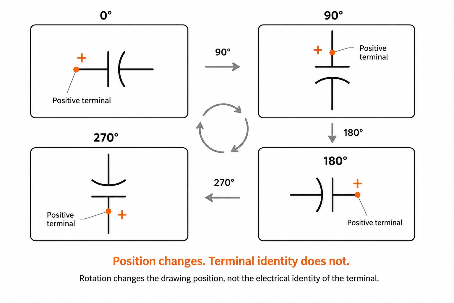
Rotating a polarized capacitor symbol changes where the symbol will appear on the page, but it does not change which terminal has polarity. The plus-marked terminal could be located to the left, right, top, or bottom of the symbol after being rotated; the terminal pin identity and connectivity are what truly matter.
When reading a symbol that has been rotated, take four steps: First, find the polarity cue; Second, find the terminal pin; Third, trace the net; and Finally, go to the project library definition. These four steps will work regardless of the position of the symbol on the page.
Mirrored or nonstandard drawings should be treated the same way as rotated symbols, so do not take a shortcut or make an interpretation for the left side or top side. If you cannot locate the pin number, refer to the EDA tool or symbol editor; if the symbol does not have an assigned terminal, you cannot reliably map it to a footprint.
What Changes Between a Schematic Symbol and the Physical Capacitor?
The schematic symbol is logical; package markings are physical and specific to the package. Between a schematic symbol and the physical capacitor are many different types of artifacts.
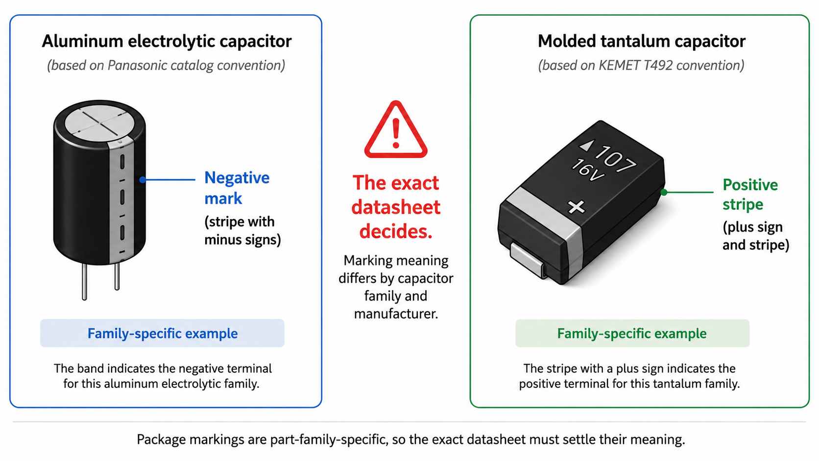
The manufacturer documentation shows the necessity of verifying the physical mark by the precise family. Panasonic uses negative polarity markings in its aluminum electrolytic capacitor catalogs. By contrast, the KEMET T492 Tantalum Datasheet uses a stripe or a plus marking to identify the positive terminal; however, the same mark means a different thing according to which family is indicated on the BOM.
For this reason, the generic product photo is not a valid substitute for the datasheet package view; the stripe's meaning is based upon the specific family and package assigned to the capacitor, not the capacitor category as a whole.
Electrolytic capacitors are comprised of different attributes, such as ESR, tolerance, voltage rating, selected case sizes, and product selection suitability—all of which reside in the project's attributes, the BOM, and the component's manufacturer documentation. Therefore, the symbol conveys none of this information.
How Do You Verify Polarity Before PCB Assembly?
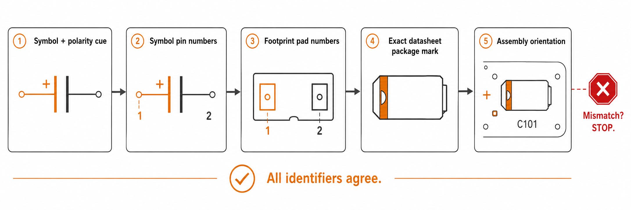
To validate polarity prior to PCB assembly, you must verify every transition by matching it to an exact artifact. The KiCad documentation specifies that the symbol pin number must match the corresponding footprint pad number, and Altium's component validation rules state that invalid pin mapping will lead to a violation that will need to be resolved—regardless of the EDA solution you are using.
The following five-step release verification check can be used:
- Identify and document which symbol variant and cue were used (e.g., whether the symbol was a generic form, polarized, variable, or trimmer). For a polarized symbol, identify and document the explicit mark as well as any specific conventions held within the project library.
- Record the actual pin numbers of the symbols. Open the library definition for your project. Do not assume the number from the left or right position of the pin.
- Match the symbol pins to the footprint pads. Verify all the logical pins are mapped to the corresponding numbered copper pads. The KiCad Schematic Editor documentation describes this relationship using numbers.
- Use the manufacturer’s documentation to check the selected MPN, pinout, type of package, and marking on the part, and determine if you are looking at a top view or a bottom view drawing.
- Verify that the outputs of the release match through the silkscreen, assembly drawing, BOM/MPN, and placement orientation. All should identify the same physical direction.
The release is not complete until every transition connects a library-defined component with a numbered pin or pad, an exact document for the MPN, and an approved assembly orientation; just having a memory reference or generic image of the icon does not satisfy this requirement.
For releases that will be manufactured, hold onto the symbol name, footprint ID, mapping from pin to pad, the MPN, datasheet revision, package-view direction, and approved placement orientation for future library or sourcing updates.
If you need to fix the mapping between the symbol and footprint, PCB design services can assist you with correcting the library chain before the release goes out. DFM and DFT reviews and SMT assembly can then proceed using the approved symbol, footprint, MPN, and orientation outputs instead of creating a new polarity definition from the beginning.
Frequently Asked Questions
Q1. What does µF mean on a capacitor?
µF refers to microfarads (µ is the prefix denoting 10^-6, and F is the unit for farad). Therefore 10 µF is a capacitance value. To convert units: 1 µF = 1,000 nF = 1,000,000 pF.
Q2. Is capacitance C or F?
Capacitance is typically represented as C, whereas its SI unit is the farad (F). However, in a schematic reference, such as C1, C will refer to the reference prefix and not the unit. In this case, read the notation “C1 10 µF” as capacitor instance C1 with a capacitance of 10 µF.
Q3. What is the capacitor symbol on a multimeter?
On a digital multimeter, the icon that resembles a capacitor is used to select capacitance measurement mode; this is an instrument control symbol separate from the schematic component designation. Because some multimeters have a dial position shared among different functions, consult the owner’s manual of your specific model to know how to select capacitance mode, as indicated by recommendations from the manufacturer Fluke.
Conclusion
A capacitor symbol on a schematic indicates a class of logical component. Carry forward that logical identity in all aspects of your projects for proper PCB assembly. Utilize the manufacturer’s designated polarity markings and the proper pin identification of the manufacturer’s parts and not merely their established position on a physical page layout. Examples from Panasonic and KEMET support the final point; a package stripe is not universally recognized as indicating polarity without reference to the component’s official part family documentation.
References & Sources
- IEC 60617 Graphical Symbols for Diagrams – IEC
- IEEE/ANSI 315-1975 – IEEE
- JIS C 0617 Graphical Symbols for Diagrams – JSA
- C Symbol Library File – KiCad
- C_Polarized Symbol Library File – KiCad
- C_Polarized_US Symbol Library File – KiCad
- C_Variable Symbol Library File – KiCad
- C_Trim Symbol Library File – KiCad
- Schematic Editor – KiCad
- Workspace Component Validation – Altium
- The International System of Units, SI Brochure – BIPM
- Aluminum Electrolytic Capacitors – Panasonic Industry
- T492 Solid Tantalum Chip Capacitors – KEMET
- How to Measure Capacitance – Fluke