Upload BOM & Gerber

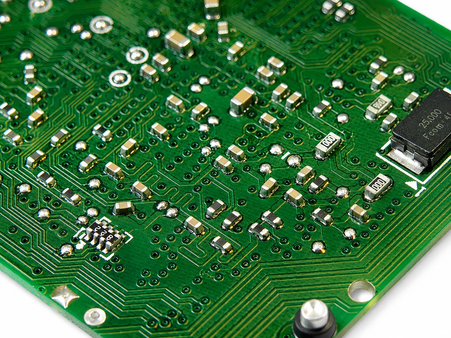
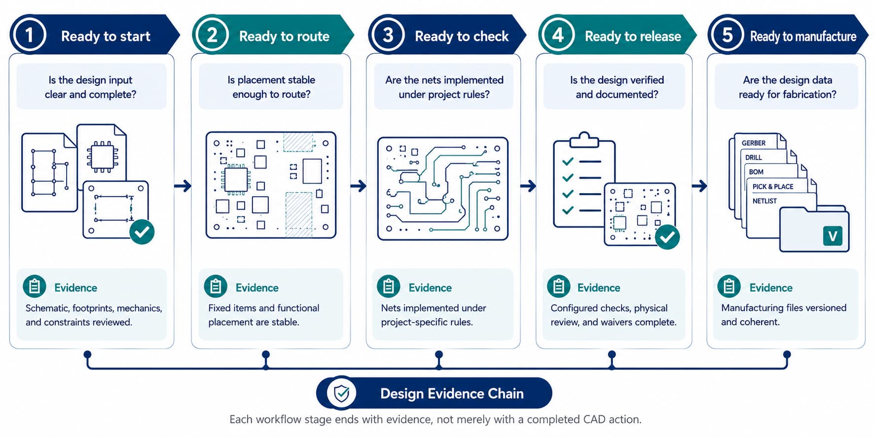
PCB layout, which converts the schematic connections into the physical layout of a PCB, is a critical step in creating an electronic product. The PCB layout includes the footprint for each component, how copper traces and vias connect them, and how power and ground are supplied. The layout also defines the data required for communication with the other stakeholders involved in creating the PCB. As such, the completed schematic should be thought of as an input to PCB layout, not as confirmation that the PCB can go into production. To assess whether the PCB has been laid out properly, do not simply check that all nets have been routed. The most important thing is to verify that the PCB project has passed through all five gates: ready to start, route, check, release, and manufacture. This article focuses on answering the technical questions that PCB layout designers need to consider as they move through their projects; however, if PCB projects include aspects such as library control, ownership of the layout, and a separate technical handoff between engineers and sales representatives, additional PCB design services may be required.
- PCB layout is the physical implementation of electrical intent.
- The first step in PCB layout is to establish stable mechanical and functional blocks; routing follows afterward.
- A clean DRC report means only that the checks enabled in that particular DRC setup have passed.
- Release packages are produced to the specification of each recipient, and fabrication, assembly, and mechanical files must remain aligned on revision, variant, origin, rotation, and documented exceptions.
Contents
show
What Is PCB Layout?
PCB layout is defined as the physical stage of the electronic design process. PCB layout is the stage where the components and interconnections of the design are assigned physical geometry. It does this by transferring the net connections created in the schematic to the board outline and defining footprints, copper tracks, vias, planes, masks, and other layers used for manufacturing the PCB. This allows the manufacturer to reproduce the required board geometry.
Connecting device pins in a PCB schematic means that the schematic represents a logical electrical connection between the pins. PCB layout represents where the pins will reside in space, how the connection reaches the pins, and the physical characteristics of the connection. This layout is important because it affects how electrical currents, signals, and heat will flow, as well as test access, enclosure fit, and manufacturability.
Integrated ECAD tools allow direct synchronization of schematic and board data. KiCad, for example, can update the PCB from the schematic to transfer footprints and net connections. For this reason, manually importing a netlist is not a universal step in a modern integrated workflow.
A visually appealing layout may still contain an incorrect footprint, an inaccessible connector, an unsuitable rule set, an incomplete output package, or an unmanufacturable design. The visual arrangement alone does not determine whether the layout is correct; the electrical, mechanical, and manufacturing intent of the PCB must be preserved during the layout process.
Types of Circuit Board Layouts
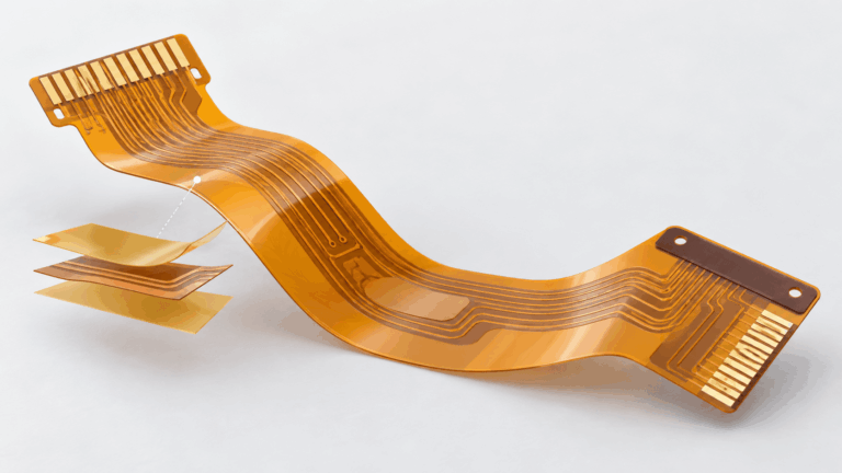
PCB layout changes with the physical construction and interconnect density of the board. The categories below are not mutually exclusive: a PCB may be both multilayer and HDI, or both multilayer and rigid-flex. Each still follows the same layout workflow, but the dominant constraints change with board structure.
High-speed, RF, and high-current layouts are not separate physical board types; they are electrical design conditions that can apply to several of the structures above. The board type should therefore be identified before critical placement and routing because it affects the stackup, constraints, mechanical model, routing strategy, and manufacturing review used in the later layout gates.
Where Does Layout Begin and End?
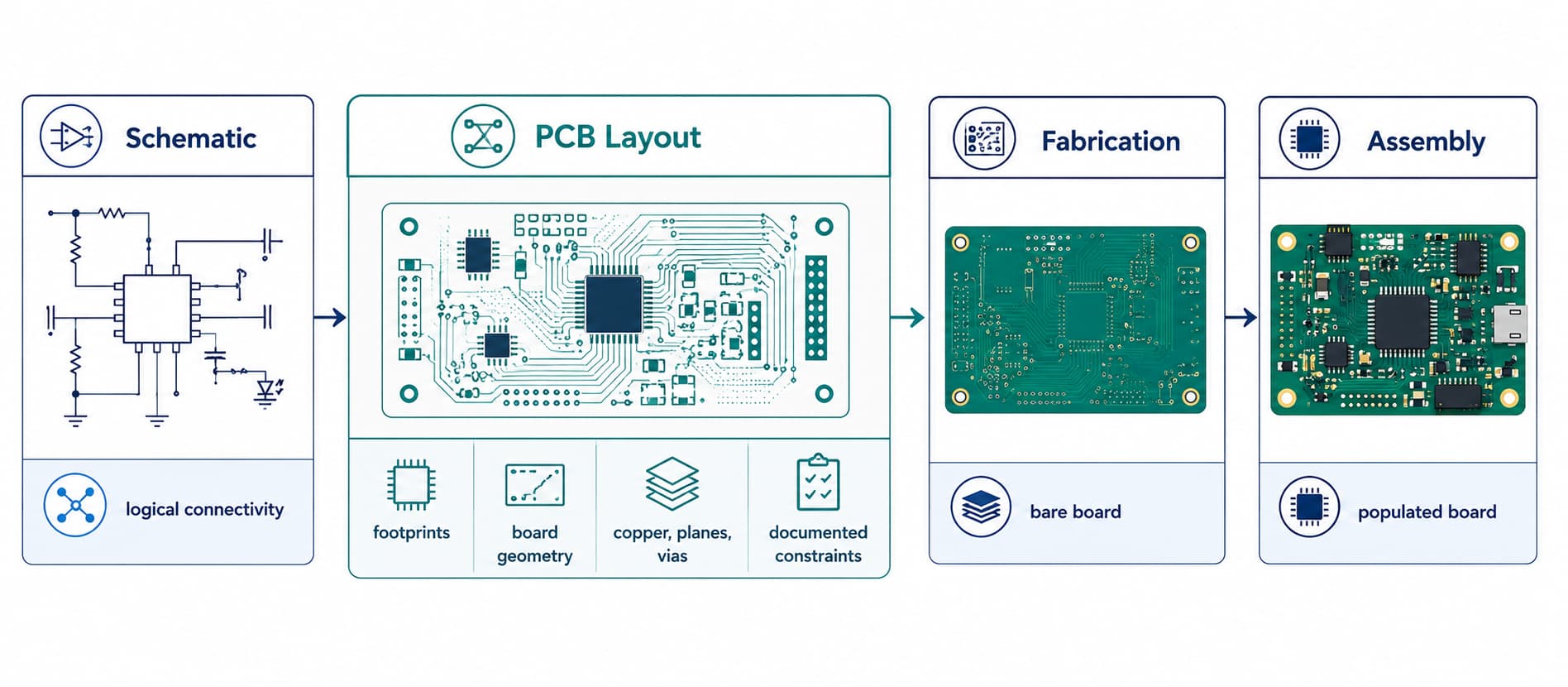
After circuit intent and mechanical constraints have been established sufficiently to provide geometric direction, the final PCB layout will yield an established board database for inspection, as well as reviewed design data for release. The process of fabricating the bare circuit board will yield the physical structure of the completed PCB; assembly will provide mounting and processing for the various components of the finished product. These processes will share information with each other; however, they will not own the same design decisions. Connection logic, part numbers, and design intent are documented in the schematic; the physical realization is owned by PCB layout. When preparing the PCB through CAM, a fabricator can modify production tooling and panels; however, the fabricator should not modify the circuit intent without consulting the designer. Assemblers will use the bill of materials (BOM), placement data, drawings, and PCB information provided by the designer to complete the chosen configuration of the PCB.
The above description highlights the two most common mistakes that occur in conjunction with PCB layout: layout should not be viewed as a mechanism for resolving issues found in an undocumented schematic, and files exported for use by manufacturers do not transfer responsibility for unresolved footprints, polarities, mechanics, or variants to the manufacturer.
Altium also follows this workflow; the PCB design workflow moves from schematic evaluation and part data through to implementation of the PCB. Each stage of PCB design should provide inspectable data that can be verified; it is not appropriate to proceed with PCB implementation based on undocumented assumptions.
Are the Inputs Ready for PCB Layout?
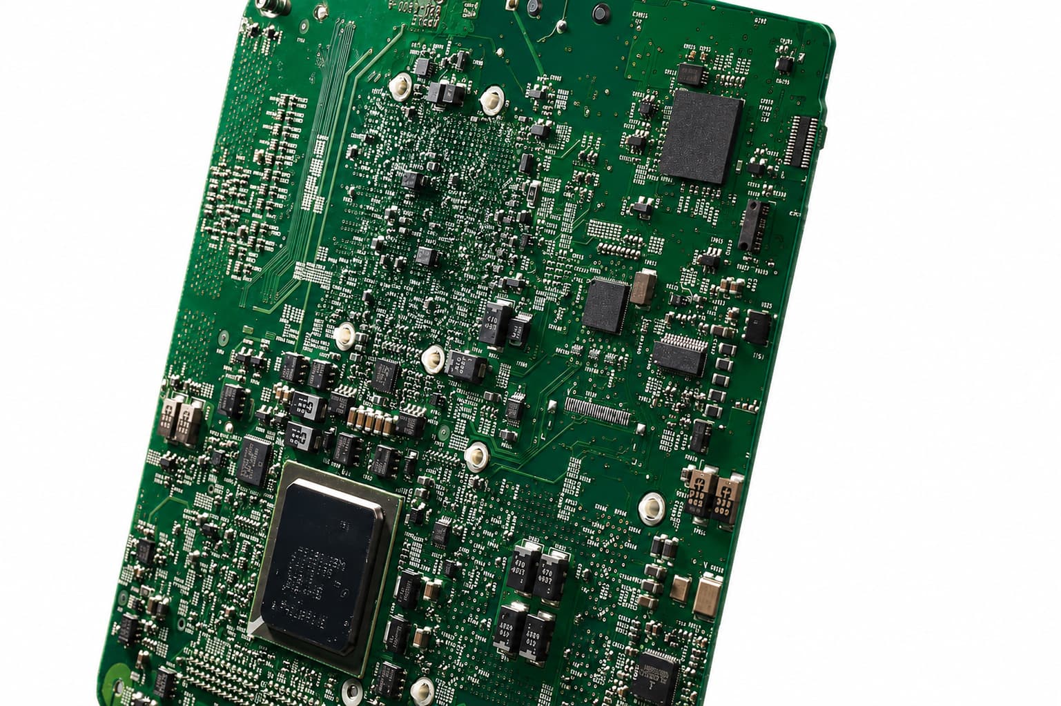
The inputs for PCB layout must be available at this point. When the inputs for PCB layout are no longer dependent on estimates or assumptions about load-bearing facts, the inputs have met this criterion. Inputs for PCB layout should be reviewed for at least the schematic, component and footprint data, board outline, connector locations, enclosure limits, mounting features, stackup direction, and manufacturing constraints.
Items that remain undetermined at this point should have a named owner and an explicit stop condition.
The layout database should include the component symbols and their corresponding footprints, in addition to the critical component data for the intended package and variant. The mechanical inputs for the project must identify the usable outline, holes, edge restrictions, height limits, and any fixed interface points. At this point in the project, a stackup does not need to follow a standard recipe, but it does need to be determined early enough to configure the layers and applicable rules. Once an acceptable preliminary stackup has been completed, the PCB layout will build on the preliminary stackup, which will contain signal layers, adjacent reference planes, copper weights, dielectric thicknesses, and controlled-impedance requirements. If the stackup is later modified, the changes will affect trace geometry, via transitions, return paths, and manufacturing constraints. Critical routing should use a preliminary stackup reviewed with the intended fabricator.
The assignment of constraints must have a name and a defined scope. Board-wide defaults are a baseline; the named constraints must reflect the requirements of the project. PCB design rules identify the various constraints on a PCB and why they may apply only to specific objects, nets, classes, or layers. A width, spacing, or via rule that does not state its scope will not provide complete information.
Before opening the routing tools, use an acceptance table to define the requirements for routing.
Silkscreen items and noncritical support parts may still move after initial placement. However, once broad routing has begun, the PCB outline, primary connectors, critical footprints, and stackup choices should be fully specified and should not remain fluid.
Place the Board Before You Route It
Placing the components of a printed circuit board before systematic routing begins establishes the physical organization of the board. When placing the components, you must first define any mechanically constrained items and then place the functional blocks based on electrical paths, power flow, thermal performance, assembly access, etc. Placement is considered complete when the remaining movement of components is controlled and can be reviewed, regardless of how tightly the components are packed.
Mechanically constrained items, including connectors, mounting holes, switches, displays, sensors, antennas, and enclosure interfaces, should be locked or clearly marked after mechanical agreement. After resolving the mechanical constraints, you will want to group the components based on their function, which will require you to refer to the schematic and current flow rather than treating the board as an empty puzzle. Datasheet geometry, loop area, thermal transfer, electrical isolation, and interface timing are some of the criteria that drive component positioning. In addition, place decoupling components close to the device power pins and within the intended current loop, rather than simply placing them around the IC outline. You should keep high-current switching nodes and loops as compact as possible. In addition, separate sensitive analog or RF nodes from noise-producing components. Reserve available copper area or airflow for heat-dissipating components. The required conditions will vary from circuit to circuit; therefore, generic priority lists cannot substitute for the documented requirements and engineering reviews for a particular device. Additionally, you may find that even ordinary support parts can move during iteration when critical paths are identified.
Placement reaches its exit gate when reviewers can identify the fixed mechanics, functional blocks, critical paths, power-conversion areas, return-path requirements, keepouts, and access requirements. Therefore, if moving one connector would require significant changes to the routing of the other components on the board, it is too early to begin systematic routing.
Route Nets Under Project-Specific Constraints
Routing is performed according to the defined constraints for each net, class, layer, and physical region. Therefore, routing can be prioritized based on which paths offer the least flexibility, while preserving intentional power and return paths when completing the remaining lower-risk connections without weakening previously approved geometry. Each defined constraint should correspond to an actual requirement within the circuit, stackup, component documentation, manufacturing capabilities, or an approved engineering decision rather than only a default supplied by the CAD tool. Exceptions should be recorded intentionally so that future reviewers can differentiate between accepted deviations and overlooked violations of the established rules.
Power and ground require a design-specific answer even within a generic workflow. Therefore, the copper on an individual board should be designed to carry the intended current and return current along the defined paths and should not force current through unintentional bottlenecks or detours. When a signal crosses from one layer to another, ensure that the return path remains continuous and add an appropriate return transition when necessary. For power paths, it is necessary to evaluate pad neckdowns, plane splits, vias, and the narrowest sections of copper rather than relying on nominal trace width alone. Controlled-impedance, differential, and length-matched nets should follow the approved stackup and interface tolerances defined within the specific design and should not use generic values taken from another design. controlled-impedance, fast-edge, sensitive-timing, and high-speed layouts intended to meet electromagnetic compatibility requirements require dedicated high speed PCB layout analysis. There is a direct link between plane and return-path decisions and the radiated and conducted emissions performance of the completed design.
The routing should remain reviewable. Ensure that net classes are meaningful, that no unexplained overrides are in place, and that layer transitions are intentional. Completion of the ratsnest is useful evidence of connectivity; it does not provide any indication of footprint accuracy, minimum enclosure clearance, thermal performance, or manufacturability.
What Does a DRC Pass Actually Prove?
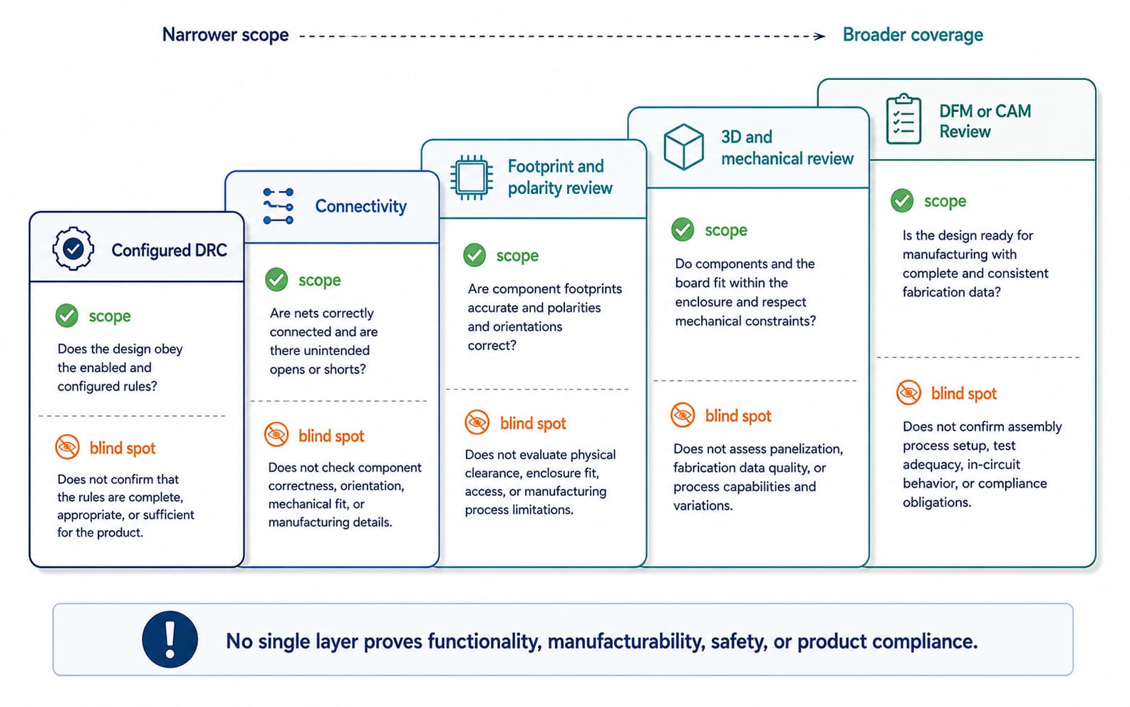
Passing DRC indicates only that the board met all enabled checks in its current configuration. This does not demonstrate that the design satisfies all project requirements, nor does it prove that all footprints are correct or that the board is compatible with the enclosure. DRC is a significant piece of evidence, but it is not a claim of release readiness. According to KiCad documentation, the design rule checker verifies that the board complies with the configured requirements and indicates connectivity issues. Not all requirements can be checked interactively. Altium information relating to DRC also states that the results represent the application of enabled rules.
Altium defines the boundaries of the board verification process through a workflow of rules and checks that finds violations against established rules, but it relies on people to ensure that the proper rules, parts, mechanics, notes, and exceptions are entered into the database correctly and completely.
Is the Layout Ready for Release?
Confirm the Controlled Revision and Open Issues
Release readiness requires independent checks to agree on the same controlled board revision and confirm that there are no unresolved issues. The release verification should consist of a review of the board database and not just the exported PCB artwork. In addition to checking the board database and exported PCB artwork for correct connectivity and footprints, you should also verify polarity, mechanical fit, rule configuration, waivers, relevant documentation, and the intended assembly variant.
After you have created the required rules for your board design, you should run batch checks when the rules have been established to a point where the batch report will contain meaningful information regarding the status of the board in relation to those rules. Once you have run all batch checks, you should reconcile every remaining violation through a fix, a documented waiver, or a known non-release condition.
You should verify the appearance and fit of the board using a 3D model of the mechanical assembly together with the best mechanical model available. You should also inspect any items that may be simplified in the component models. These items include cable access, mating direction, hardware positioning relative to the board, and process-clearance requirements.
Perform Mechanical and Human Review
If the complexity or risk of the board warrants a second qualified review, the individual performing the release verification should have access to the schematic, manufacturing constraints, mechanical inputs, variant information, change history, and known exceptions. The lack of documentation tied to the current board revision is an inadequate basis for release verification. A simple screenshot or verbal approval would be considered weak documentation.
Designers experience many common failures when releasing their designs: the wrong footprint is used with the correct schematic symbol; connectors are fixed before enclosure agreement; large loops are used to connect decoupling capacitors; current paths narrow at pads or vias; signals cross reference-plane gaps; routing rules are created but not applied to the intended nets; and the Gerber files, BOM, placement files, and assembly files are generated from different revisions. Details that automated geometry checks may not identify include silkscreen legibility, fiducial access, courtyard conflicts, exposed copper, tooling margins, mating envelopes, fastener reach, and service clearances.
The inspection should include samples of annular rings, solder-mask dams, paste apertures, reference-designator readability, test-point accessibility, copper-to-edge geometry, thermal reliefs, plated slots, panelization assumptions, depaneling zones, and fabrication notes.
Review Special Features and Manufacturing Risks
Special features such as microvias, press-fit holes, backdrilling, rigid-flex transitions, and thermal coins require feature-specific review. General board-wide DRC will not fully reflect the stackup dependencies, clearances, and process tolerances of these features.
IPC provides PCB design standards as a framework of requirements for board design and documentation. IPC treats manufacturing evaluation for design for manufacturability (DFM) as a separate activity. Therefore, supplier-facing DFM review should test the released board data against the selected manufacturing process rather than being treated as another name for CAD DRC.
Organize the Manufacturing Handoff by Recipient
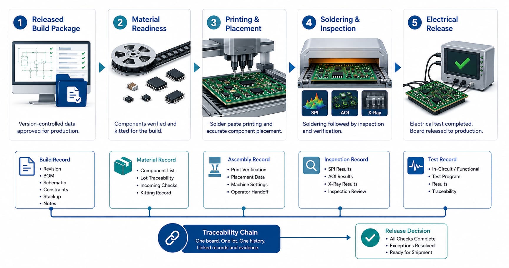
The release process for manufacturing must be structured around the different recipients of the files rather than as a single package that includes everything in one undifferentiated folder. Fabricators, assemblers, and mechanical reviewers need different types of documentation to complete their tasks. Each package must reference the same revision and variant, identify the coordinates and units using documented information, and agree with the design data used to generate the output documents.
KiCad supports the generation of Gerber, drill, IPC-2581, ODB++, position, BOM, IPC-D-356, and other outputs. Altium separates fabrication output documents from assembly output documents and identifies supporting mechanical or test deliverables. It is more important to ensure that the output files match the same board revision and assembly variant than to create an output in every format available for export.
Populate the data through detailed documentation and follow up by confirming with the fabricator all required formats, along with any process limits to be used before exporting. Generate all outputs from one controlled source revision of record. A Gerber set from one revision and drill data from a different revision could create different hole placement. A bill of materials (BOM) and placement file from different variants could create placements for do-not-place (DNP) parts. An undocumented origin or rotation convention could misplace components. It is important never to repair one file without confirming that it matches the source database and the entire package. Maintain an archive of the release manifest with filenames, revision, variant, generation date, approved exceptions, and recipients. Reopen or regenerate representative outputs before transfer.
Frequently Asked Questions
Q1. Can a beginner design a PCB layout?
Yes, a beginner can create a simple, low-risk circuit board layout after learning about circuits, footprints, mechanical requirements, and manufacturing limits. You should begin with a bounded design and use the five gates to identify unknowns. A person experienced in designing PCBs for high-power, high-speed, RF, safety, or densely constrained mechanical projects will need to verify the layout because of these design constraints.
Q2. Which PCB layout software features matter most?
The most useful PCB layout software features include reliable schematic synchronization, controlled libraries, board and stackup configuration, scoped rules and classes, interactive and batch DRC, connectivity verification, 3D or mechanical review, revision control support, and standardized fabrication and assembly export capabilities. PCB layout software should be chosen based on the evidence required by the project, not the length of its feature list.
Q3. What is the difference between a PCB schematic and PCB layout?
The schematic identifies components and shows how those components are logically connected, while the PCB layout takes the schematic connections and converts them into footprints, board geometry, copper routing, vias, planes, keepouts, and all manufacturing layers for the PCB. Each carries a different type of risk—an error in the schematic indicates a design defect that can be identified during the schematic review process before PCB layout begins. Conversely, a PCB layout can create a PCB that accurately represents a flawless schematic but is still incapable of performing as specified in the field.
Q4. Does passing DRC mean a PCB is ready for manufacturing?
No. Passing DRC only indicates that the PCB layout satisfies all enabled rules within the DRC rules manager under the current configuration. To be considered ready, a PCB layout must also pass footprint and polarity checks, mechanical fit checks, assembly clearance checks, and other applicable reviews. In addition, assembly variants, documented exceptions, fabrication constraints, and the Gerber, drill, BOM, component-placement, and drawing files must be consistent.
Conclusion
An acceptable complete PCB layout will preserve the PCB’s electrical, mechanical, and manufacturing intent and provide the manufacturer with a record of the design decisions made regarding the PCB layout. The design decisions should also be supported by stable inputs, reviewed placement, scoped constraints, independent checks, and coherent manufacturing files. The release package will provide the manufacturer with the evidence needed to release the PCB for manufacturing. When a gate fails, refer back to the source decision rather than continuing to improve the downstream output after routing. This will keep the routed PCB from appearing more mature than the evidence and provide the reviewer and manufacturer with a controlled basis for the next decision.
References & Sources
- PCB Editor – KiCad
- How to Design a PCB: From Schematic Capture to Manufacturing – Altium
- Defining, Scoping and Managing PCB Design Rules – Altium
- Design Rule Checking – Altium
- Verifying Your Board Design – Altium
- Overview of PCB Design Outputs and Manufacturing Files – Altium
- IPC Board Design Standards – Global Electronics Association
- Design for Manufacturing Confirmed by IPC Standards – Global Electronics Association
- What Is PCB Layout? – Cadence
- Introduction to Printed Circuit Board Layout for EMC – LearnEMC