
Upload BOM & Gerber


The main difference between a rigid PCB assembly and a Flex PCBA assembly is mechanical because the substrate may move during the various steps of the flex assembly process: printing, placement, heating, connector insertion, inspection, separation, and final use. A process that works on rigid PCB assemblies has the potential to create registration errors, localized strains, and a false sense of reliability when it is implemented on a Flex PCBA assembly without proper controlled support throughout the assembly process.
Bare FPC fabrication and Flex PCBA assembly are distinct manufacturing stages. The product is identified using the Gerber file data, BOM, and centroid X, Y coordinates, but they do not describe critical items such as bend duty, stiffener transitions, tooling support, formed-state loads, and motion-life acceptance. Those parameters determine whether an apparently good Flex PCBA will remain functional once it is installed or moved repeatedly.
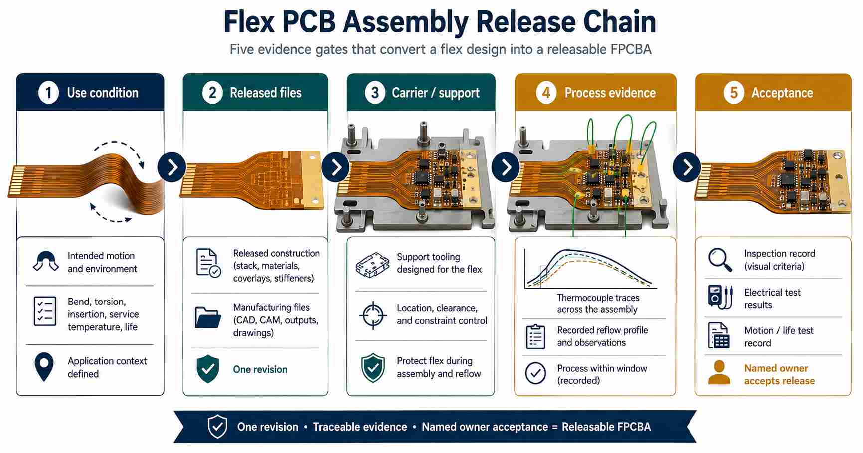
Flex PCBA is production-ready when the flexible circuit construction, intended motion, tooling support, measured thermal process, inspection route, and product-specific acceptance criteria are in agreement. Bend ratio, bake cycle, and oven settings also depend on the material construction and operating conditions and should not be treated as universal rules.
Contents
show
What Is Flex PCB Assembly?
A Flex PCBA is a flexible circuit assembly after electronic components, including connectors, have been soldered onto it and other hardware has been mounted onto the Flex PCBA. A bare circuit can be made as a single-sided, double-sided, or multilayer FPC. When a rigid-flex FPC assembly is created, the flexible areas of the circuit are combined with rigid sections that give mechanical support to certain areas of the assembly.
The basic steps for FPC circuit assembly include preparation of materials, solder paste printing, placement of components, soldering, inspection, electrical verification, and handling after separation from the assembly.
The mechanical assumptions made about the assembly steps change the way the assembly must be supported. In a rigid circuit assembly, it is generally assumed that the circuit will maintain its shape. When using a flex circuit assembly, however, the flex circuit can wrinkle, shift during stencil printing, droop while under the placement nozzle, deform in a carrier, or transmit insertion force into a copper transition. Therefore, the means by which assembly is performed dictate where the circuit remains flat, where it may bend, and how the force travels from the components or connectors into the moving portion of the assembly.
Flex circuits can be constructed using polyimide as a dielectric; however, the specifications of the overall material system used to create the FPC assembly are more important than just the polyimide material. For applications where flex circuits will undergo repeated flexing, a common selection for the copper used in the production of the circuit is rolled-annealed copper. This type of copper is better suited to cyclic deformation than conventional electrodeposited copper. Flex life is determined by all of the above-mentioned variables acting together; thickness, trace direction, bend radius, neutral-axis position, stackup, cycle conditions, and the type of copper are part of the same calculation rather than a sequence.
For example, the static folding of a display tail into an enclosure creates a static installation. The installation of a serviceable module that is opened for maintenance creates a limited number of cycles, while a camera hinge, robotic joint, or moving sensor head creates true dynamic duty. All of the above applications for flex circuits may use similar construction materials for the assembly, but the support required during assembly, acceptance test protocols, and design features will differ.
How Motion Duty Changes the Assembly Plan
The first decision is not a generic minimum bend radius. It is how the finished assembly will move, where it must stay rigid, and whether electrical performance must be maintained while it moves. Static, limited-service, and dynamic duty create different failure mechanisms and therefore require different test evidence.
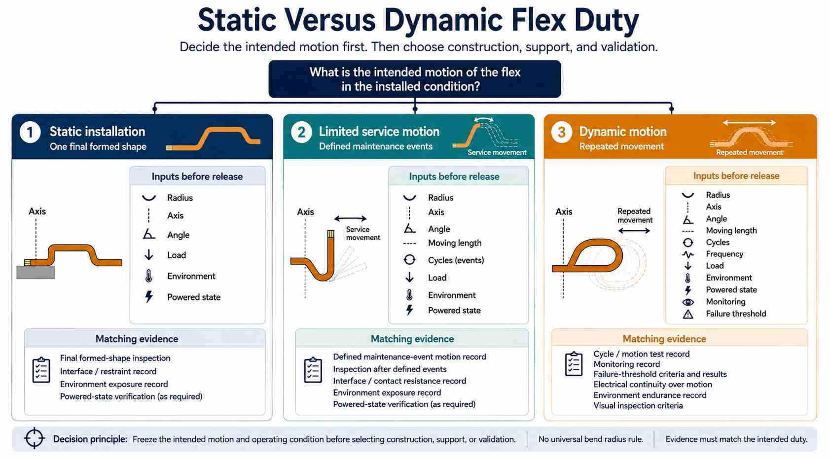
The bend ratio is determined by dividing the bend radius by the total thickness of the circuit. The published bend ratios by Minco are as follows: Single-Layer Circuits for a Static Application have a minimum ratio of 10:1. Double-Layer Circuits for a Static Application have a minimum ratio of 10:1. Multi-Layer Circuits for a Static Application have a minimum ratio of 20:1. If a bend ratio is applied tighter than the published ratios, such as treating a 10:1 ratio as sufficient for multi-layer circuits in a static application, the copper layer may be subjected to a higher level of strain than what it has been qualified for, which can result in cracking that does not occur until long after the unit has been shipped and put into normal use. The published bend ratios are not hard limits for all designs and should not be viewed as limitations on every manufacturer’s copper layout, adhesive system, stiffener transition, or dynamic product. A fixed millimeter value without a total circuit thickness or a defined duty cycle can be misleading.
IPC-2223F is the 2026 revision of the sectional design standard for flexible and rigid-flexible printed boards. IPC-2223F provides sectional design requirements and guidance. However, the actual geometry of a printed board must be defined by the product drawing, approved construction, and validated testing of the final assembly for its application, and not by the IPC-2223F design guidelines alone. For dynamic acceptance testing, define the radius, axis of bending, angle of bend, moving length, bending rate, total load during dynamic acceptance testing, environment where the dynamic acceptance test is performed, powered state, and the method used to monitor performance during the dynamic acceptance test. The total number of cycles needed to accept the assembly as a dynamic assembly with a confirmed failure threshold must also be included in the requirements. An assembly that is seen as having a value of zero ohms sitting idle on the workbench has not completed the required dynamic testing to demonstrate performance in a moving joint.
Which Design Inputs Must Be Final Before Tooling?
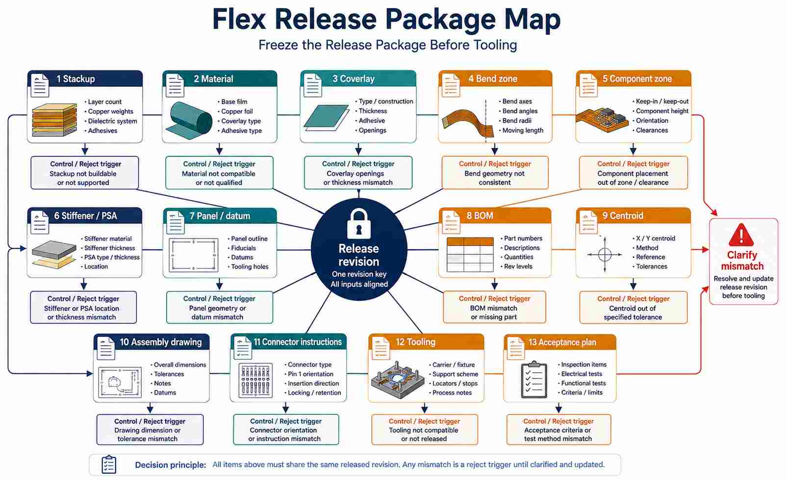
Tooling should not be created based on multiple file revisions. An example would be tooling created against the previous revision of a carrier for a panel whose coverlay opening has moved half a millimeter from the stiffener edge in the current release. This error would not be obvious because the support would be applied slightly incorrectly, which could lead to a local buildup of strain that may not result in failure until after the assembly has been shipped and put into use. The effect on a flex circuit can be more significant because minor changes in coverlay openings, the stiffener edge, or bend zones will affect not only how the tooling contacts the circuit but also how strain is distributed.
The definition of PCB handling encompasses both the material condition requirements of the PCB itself and how the PCB will be handled, stored, transported, and processed. The IPC-1602A document outlines procedures for handling and storing printed boards, including how to prevent contamination, mechanical damage, solderability deterioration, ESD, and excessive moisture pickup.
While IPC-1602A does not assign a specific MSL to printed boards as a whole or define a universal floor-life and bake recipe, manufacturers should refer to their PCB supplier’s instructions, as well as the condition of the packaging, the exposure history of the package and the PCB itself, and any available condition data. Conditioning decisions should be based on these factors and the risks introduced by unnecessary baking.
How Should the Carrier Support the Flex Panel?
A Flex Panel must remain in a repeatable mechanical position during process steps in which movement can affect solder paste registration, component placement, solder-joint loading, or inspection. For that reason, the same physical fixture does not need to remain on the PCB throughout the entire process. Each step of the process (print carrier, reflow carrier, inspection nest, test fixture) can have a different physical fixture, but each state requires validation to maintain its coordinate relationship with the approved panel definition.
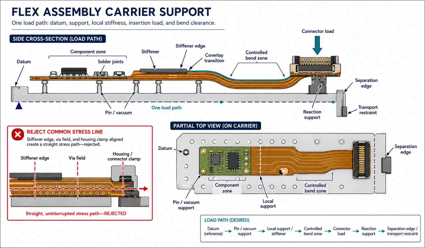
A trial PCB should be processed to verify that the circuit board is properly aligned during printing, correctly controlled during placement, passes through heating without forming any additional folds or local buckling, and is removed from the tool without causing any damage or strain. Subsequently, prior to entering volume production, the printed circuit board’s pin contacts, vacuum control points, nest points, and frame points should be checked for proper alignment to the PCB. If there has been a change in the relative position of the PCB during solder paste printing or component placement, if there are any additional folds or buckles, or if there is a mechanical load developing on a joint, the support system must be corrected prior to continuing production.
Stiffener edges, coverlay edges, via fields, copper direction changes, and housing clamps can align on the same cross-section. Therefore, these features can produce a higher concentration of strain even when each of them is individually acceptable.
Flex PCB Assembly Process
The assembly procedure for flex PCBs will continue with the same sequence as for standard SMT assemblies. However, each stage of the SMT process for flex assemblies must have flex-specific controls—if an error occurs at any stage of this process, the outcome may not be immediately apparent at the same point in time. For example, although a panel may print correctly, it can still shift during component placement and create skewed components. A solder joint may also look fine after reflow but later crack when the assembly is subsequently bent into a housing.
Material Condition and Panel Preparation
To properly store, condition, or support an FPC, first verify the exact construction of the FPC in question. Therefore, moisture control of the FPC should be managed through both packaging and exposure management, rather than relying solely on a bake cycle. If additional conditioning is required, the conditioning method used must be consistent with both the manufacturer’s instructions and the construction of the FPC. If the FPC requires conditioning, then the condition that triggered it must also be documented. Prior to loading the panel onto the carrier, it is necessary to check panel flatness, whether the attachment of stiffeners is properly done, and the locations of coverlay openings, fiducials, and tooling features.
Solder Paste Printing and SPI
Printing the solder paste will require maintaining stable contact between the flex panel, carrier, and stencil to ensure proper solder paste transfer; even if the panel appears visually flat, there may be local gaps that cause poor solder paste transfer. For SPI of the flex panel, the results will be more than just pass or fail; SPI will yield information about the area, height, volume, offset from the intended position, and whether a solder paste trend is developing on the same panel due to registration drift or lack of stability below the panel. The same registration offset of solder paste in one area of the panel may also represent an issue with the flatness of the carrier or movement of the flex panel rather than being a stencil aperture issue.
Pick-and-Place
Placement accuracy may degrade due to force exerted by a nozzle on a region of the flex panel that is not adequately supported, or shifting of the flex panel occurring between when it was measured with the fiducials and when components are placed. Critical areas of support underneath the panel must be located directly under the locations of the critical components and should not force an intended bend of the flex panel into a flattened state, as this will create residual strain. Program revisions, fiducial results, component rotations, and any limitations placed on the amount of force used during component placement must all be based on the same condition of the panel when it was first qualified.
Reflow Profiling
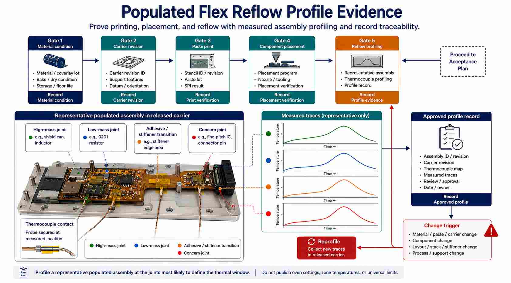
A recipe for an oven cannot verify the thermal history of a flex PCB assembly. Use thermocouples to check representative populated assemblies at joints or regions that encompass the anticipated extremes of temperature while supported in their approved condition. When measuring the assemblies, include both areas with high mass and areas with low mass, as well as any areas containing connectors, stiffeners, adhesives, or supports where the process window may narrow. Any modifications to an assembly such as carrier material, carrier thickness, support area, panel construction, solder paste, component mass, or oven configuration warrant re-evaluation rather than automatically applying the old profile to the assembly.
Indium’s application note indicates that bare and populated assemblies can differ by 10°C or more during reflow profiling; this is a method-specific warning indicating the need to take measurements of the completed assembly and not rely on a single correction factor. DuPont also reports a 288°C for 10 s solder-float result for the specific test method and type of Pyralux LF material being qualified; therefore, using that result as a target profile for the entire assembly does not take into consideration all of the other thermal factors contributed by the populated board.
Connector, Through-Hole, Separation, and Handling Operations
Manually inserting connectors, working on through-holes, trimming PCBs, and depaneling them continue the same load-path issue after the reflow operation. Place support as close to the applied force as possible to reduce the potential for folding, peeling, or twisting the flex around terminations. Define the sequence in which the assembly will be separated from adjacent assemblies and how the completed assembly will be transferred or packed for shipping. A completed assembly may still be negatively affected by a newly introduced bend during manual transfer or transport of the assembly.
Common Flex PCB Assembly Defects and Root Causes
Defects associated with flex PCB assemblies may sometimes appear to be ordinary assembly defects; however, upon further inspection of their mechanical state, the cause may be associated with movement of the PCB, thermal history, or the actual load path rather than the soldering process alone.
Comparing bare-board electrical records, material and storage history, carrier revisions, measured populated-board profile, inspection results, and electrical data from before and after assembly can help determine whether the post-reflow open originated from a latent fabrication weakness, a joint problem, or an incorrect load path that became evident after bending or heat had been applied. Then reproduce any approved forming operation under controlled conditions. The location where the open appears does not by itself establish the origin of the defect.
In contrast, the fault associated with “intermittent motion” needs further testing. The fault must be recreated while monitoring the circuit using the specified radius, axis, angle, moving length, rate, load, environmental conditions, and powered state. If the fault appears only when using a different or more demanding motion than originally intended, the test may be proving an unrealistic load rather than an actual assembly defect.
How Is a Flex PCBA Inspected and Accepted?
There is no single inspection method for all flex PCBs. While the flex board may pass electrical and visual inspection while lying flat, an intermittent open may not be detected until it is folded into its actual installed configuration. Because conventional visual inspection and electrical testing methods for flat boards do not place the copper under the conditions it will encounter in the field, acceptance should reflect the actual failure mechanism rather than simply following a standard production-line methodology.
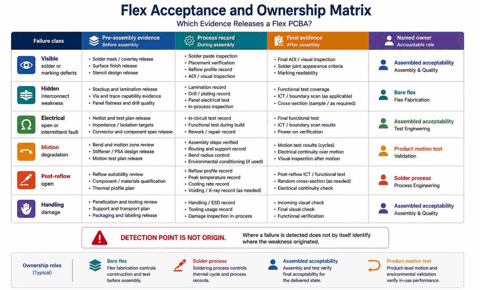
The standards set forth in IPC-A-610J apply to the acceptability of electronic assemblies. Soldering materials and process requirements are covered under J-STD-001J, while bare printed-board acceptability is covered under IPC-A-600M. When determining the qualification and performance of the flexible or rigid-flex printed circuit board itself, the applicable contractual revision of IPC-6013 should be used. Each of these standards serves a purpose and is used in conjunction; none can be used as a substitute for the agreed product drawing, the agreed class, or a motion test if the use of the product is based on repeated flexing.
In order for there to be an audit trail for the cycle results of dynamic products, the specimen and the motion must be completely identified. This includes recording the revision to the assembly, radius, axis, angle, moving length, cycle rate, load, environment, powered state, cycle count, method of monitoring, and failure criteria. Without this documentation, the headline cycle count will not provide a meaningful comparison point between manufacturers or constructions.
What Drives Flex PCB Assembly Cost and Lead Time?
The bare unit price of the FPC will only provide part of the quote; typically, a quote based on the bare unit price of an FPC may make the board seem more reasonably priced. However, once assembly begins, the cheaper board may require a custom carrier, additional labor for a manual alignment step that was not budgeted for, and another round of rework because there was no defined test plan prior to assembly. Therefore, the total installed cost of the more expensive board that does not require these three additional steps may be lower than that of the cheaper board when fully installed.
If you are evaluating potential vendors, separate one-time NRE from recurring unit costs. There may be an initial expense for the carrier, profile study, or motion fixture, but this may reduce variability and rework once the product is put into production. The lead time should be estimated based upon the approved construction, tooling maturity, available components, validation burden, inspection route, anticipated volume, and change state, rather than a fixed number of days.
Flex PCB Assembly Standards
Flex PCB assembly standards address different aspects of the overall process flow, including design, fabrication, handling, soldering, and acceptance. The applicable contractual revision of the standard should be identified within the procurement and quality documentation because using only a standard number without specifying the revision or a product-specific requirement can create ambiguity in critical acceptance criteria.
References & Sources
- IPC-2223F, Sectional Design Standard for Flexible/Rigid-Flexible Printed Boards, 2026 – IPC / Global Electronics Association
- IPC-1602A, Standard for Printed Board Handling and Storage, 2024 – IPC / Global Electronics Association
- IPC-A-600M, Acceptability of Printed Boards – IPC / Global Electronics Association
- J-STD-001J, Requirements for Soldered Electrical and Electronic Assemblies; IPC-A-610J, Acceptability of Electronic Assemblies – IPC / Global Electronics Association
- IPC-7530B, Guidelines for Temperature Profiling for Mass Soldering Processes, 2025 – IPC / Global Electronics Association
- Designing a Flex Circuit for Flexibility, 2024 – Minco
- Flex Circuit Design Guide – All Flex Solutions
- Attaching Thermocouples to a PCB for Reflow Profiling – Indium Corporation
- Pyralux LF Acrylic Sheet Adhesive Data Sheet – DuPont
- Process Guidelines to Ensure Optimal SMT Electronics Assembly – Indium Corporation
- Assembling Rigid-Flex Panels – Circuits Assembly
- Flex PCB Assembly in Factory – Makerfabs Flexible PCB Manufacturing Process – Makerfabs


