Upload BOM & Gerber

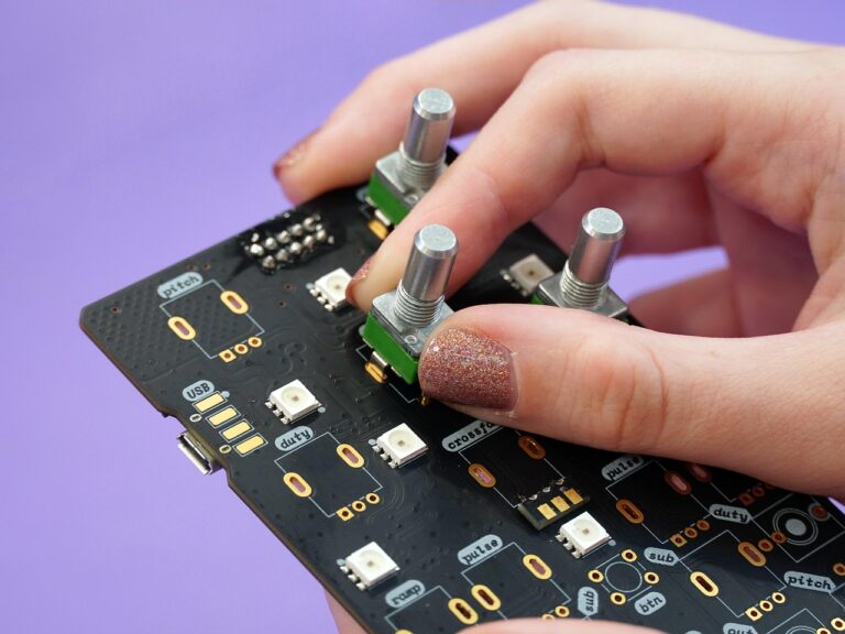
An SMD, or surface-mount device, is an electronic component that connects to pads on the printed circuit board surface. A through-hole device has leads that pass through holes drilled through the main circuit board and are soldered on the opposite side. There are many ways to join SMD components to circuit boards because they can come in several physical forms.
Many SMDs connect in similar ways: the leads from the component may be directly exposed, or the connections may be located underneath the part. However, each individual style of connecting an SMD component to a PCB is different. An SMD component may connect through the metal ends of the component, visible leads, underside connections, or solder balls. Therefore, when you read a circuit schematic, check a bill of materials, or try to identify an unmarked component, you need to understand which type of SMD connection you are dealing with.
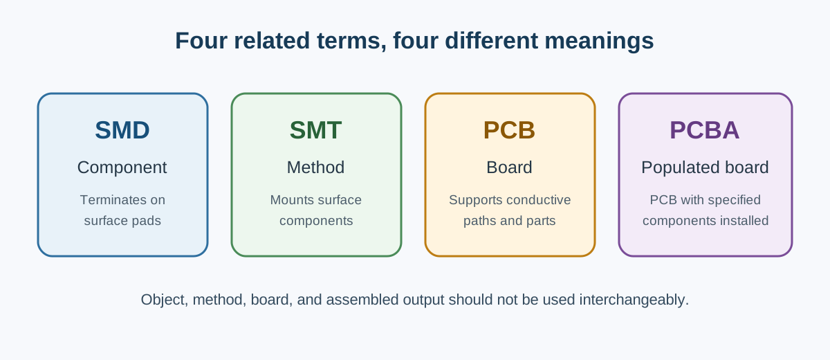
- An SMD is an electronic device that connects directly to pads on the PCB. SMT describes how the device is mounted on the main circuit board.
- An SMD may connect through metal end caps, visible leads, underside lands, or solder balls. Termination style also determines which inspection methods apply.
- Package shape and markings may rule out many options; however, a valid manufacturer part number is normally determined by matching design records or using manufacturer-specific documentation.
- SMD and through-hole components can be on the same printed circuit board because the connection method selected for each component does not limit the overall board design.
Contents
show
What Is an SMD on a PCB?
An SMD, or surface-mount device, is an electronic component whose terminals connect to pads on the PCB surface. A through-hole component instead has leads that pass through drilled holes before soldering. This distinction matters most in documents that mix the two terms casually. When an assembler sees “SMT resistor” in a BOM, they see the mounting method, not the actual part number of the component needed to build that line. The term “SMT” indicates how the component is mounted, not which specific resistor should be purchased; therefore, the part-number field in the BOM must contain the component’s true identity.

Once all the specified components have been attached and soldered to the PCB, it is referred to as a printed circuit board assembly (PCBA). “SMD” refers to the manner in which the component is connected to the PCB, not the function it serves. Therefore, resistors, capacitors, semiconductors, connectors, and switches, among others, can all be surface-mount devices.
SMD, SMT and Through-Hole Components: The Physical Difference
Many people confuse SMD, SMT, and through-hole components when referencing them in BOMs, work instructions, and repair notes because SMD and SMT are often used loosely as if they are synonymous. The following table summarizes how these three terms relate to their physical characteristics.
Connection style is a packaging and assembly choice influenced by electrical, mechanical, thermal, reliability, and service requirements; it does not define the component’s electrical function.
How Do SMD Terminations Connect to PCB Pads?
Many two-terminal chip-type parts, such as resistors, multilayer ceramic capacitors (MLCCs), ferrite beads, and chip diodes, are manufactured with metallized terminations located at each end that contact paired pads on the printed circuit board (PCB). Similar rectangular components may perform different electronic functions; however, differences in pad geometry, paste amount, or heating can cause misalignment during reflow.
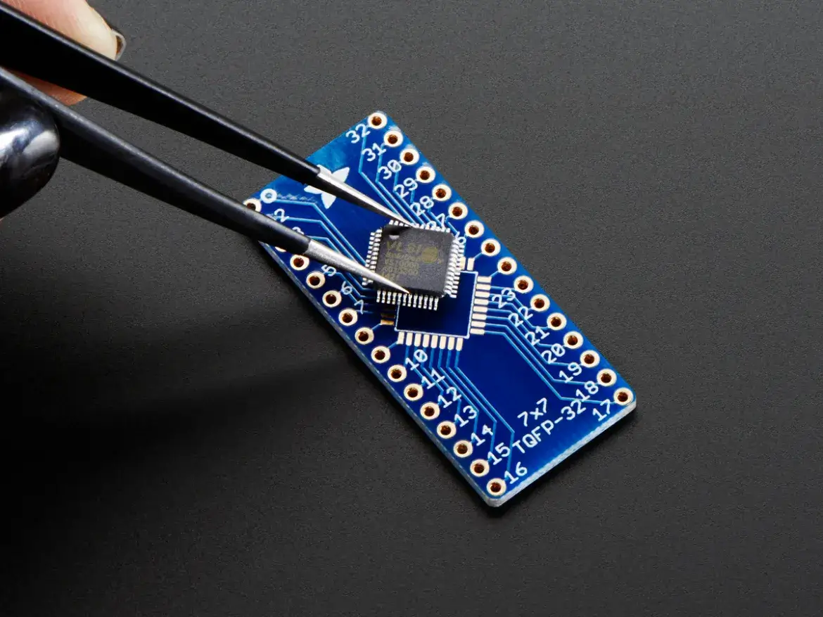
Packages such as SOT (Small Outline Transistor), SOIC (Small Outline Integrated Circuit), TSSOP (Thin Shrink Small Outline Package), and QFP (Quad Flat Package) have exposed leads that help identify the package family. The shape and number of leads help define the package family. Package drawings define the pin numbering.
Although inspection can identify problems such as bridging, bent leads, or poor pad contact, these issues do not provide any insight into what function the electronic circuit is intended to perform.
QFN (Quad Flat No-lead), DFN (Dual Flat No-lead), and LGA (Land Grid Array) packages have most or all of their electrical lands located on the underside of the package body, and they often include a central pad for grounding or thermal transfer. BGA (Ball Grid Array) and Wafer Level Packages (WLPs) use arrays of solder balls to connect to the PCB. The solder joints of BGAs and WLPs are not visible like the joints of chip and gull-wing packages; therefore, controlled paste deposition, reflow profiling, and X-ray inspection may be required for proper evaluation (Refer to: QFN and SON PCB Attachment; TN1224 Mounting Instructions for SMD Packages).
Why SMD Components Are Common on Modern PCBs
Surface-mount technology allows a higher density of components to be placed within a given PCB area. This is possible because surface-mounted devices (SMDs) do not require a lead-through hole for each terminal. Many surface-mounted devices can occupy both sides of a PCB, while tape-and-reel packaging supports automated placement. Shorter terminals may reduce parasitic inductance and capacitance; however, the package configuration, land pattern, stack-up, and routing will affect overall performance.
Higher density creates its own manufacturing limitations. Smaller pads require tighter control of solder-paste deposition and placement accuracy. Very small packages and bottom-terminated packages are also difficult to inspect and rework manually. Therefore, high density is one of many design tools that a designer can use when selecting a package for a PCB; it is not the only reason to choose the smallest size available.
A PCB does not have to use exclusively surface-mount or through-hole components. When choosing a connection style for a component, the designer will consider the size of the component, its electrical function, mechanical load, thermal path, and service requirements. For instance, most dense integrated circuits (ICs) and chip passives use SMT, while heavy transformers, terminal blocks, or connectors subjected to insertion forces typically incorporate through-hole pins or board locks. Therefore, mixed assembly is an engineering choice made at the component level and does not indicate that a product or design is outdated.
Common SMD Types and the Clues They Provide
Passive Components
Chip resistors, multilayer ceramic capacitors (MLCCs), inductors, and ferrite beads are passive electronic components that often have rectangular bodies with metal end terminations. While a reference designator such as R, C, or L indicates the intended component category, the datasheet contains the technical specifications for each component.
Selecting a chip resistor involves many different factors, including resistance value, tolerance, power rating, temperature coefficient, voltage rating, and pulse capability. Only chip resistor packages large enough to hold printed codes will contain them, and manufacturers provide package markings according to their marking policies for documented resistor families and sizes (FAQs about Surface Mount Resistors; Surface Mount Resistors Marking).
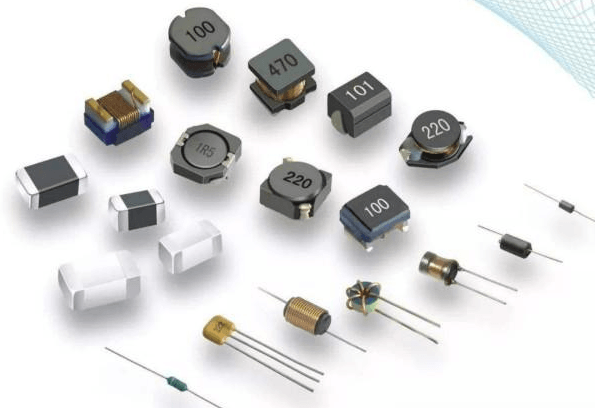
Ordinary and three-terminal MLCCs are non-polarized. Low-ESL capacitors with three terminals are non-polarized, but their through and ground electrodes must conform to the manufacturer’s drawing (Do chip multilayer ceramic capacitors have polarity?). Capacitance, voltage, dielectric, package size, and temperature characteristic also matter, and high-dielectric-constant MLCCs can lose effective capacitance under DC bias (DC Bias Characteristics of Ceramic Capacitors).
The chip body outlines of a ferrite bead and an inductor can look very similar; however, their impedance characteristics and intended circuit functions are quite different, making it critical to use the schematic and complete manufacturer part number to differentiate between filtering and energy-storage applications rather than relying on physical characteristics such as color or size.
Semiconductors and Integrated Circuits
This section covers the differences between discrete semiconductor devices, such as diodes and transistors, and integrated circuits (ICs), which are devices that contain many functional elements within one package. An identical package style may assist in narrowing the possible application of a part; however, devices in identical packages can have different functions, pin assignments, voltage ratings, or internal circuits. Terminal count, case family, manufacturer top marking, logo, chamfer, polarity band, or dot may help narrow the candidates.
This can be seen in the SOT-23 package, which is used for diodes, bipolar transistors, MOSFETs, ESD protection devices, and many other small semiconductors. All of these devices can use a three-terminal outline, which does not indicate the function or pinout. Pin identification must be based on the relevant SOT-23 package drawing (SOT23 Package). A cathode band, pin 1 identification dot, or beveled corner has meaning only within the appropriate package drawing.
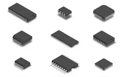
The top marking of an integrated circuit may also combine an abbreviated device code with a lot number, production date, or grade information. Therefore, it is important to ensure that the manufacturer and product family match when using a marking lookup (Packaging Part Marking Lookup). A QFN exposed pad can provide ground, heat transfer, or both, whereas BGA solder-ball joints require a different inspection method from visible leads.
Electromechanical Parts
Some electromechanical components, such as surface-mount switches, connectors, relays, and similar parts, have electrical connections as well as a mechanical interface. A switch must have the proper actuation type, contact arrangement, direction, force, and operating life for the intended application. A connector must be able to mate with the appropriate connector family, have the correct pitch, contact count, keying, orientation, current rating, and mechanical locating features.
While having similar footprints for both the part in question and the printed circuit board (PCB) where the part will be mounted may assist in determining whether they will fit together, footprint similarity does not guarantee compatibility. The PCB land pattern and external mechanical interface must also match. A reference designator identifies the circuit location. The comment or manufacturer part number describes the intended component. The footprint defines the mounting pattern of the intended component (ActiveBOM).
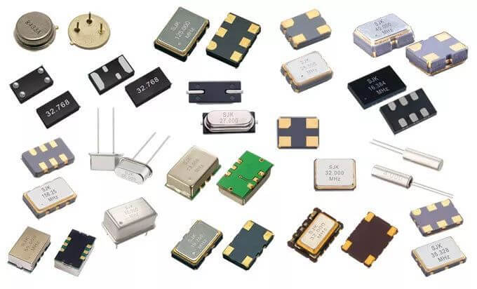
Connectors can be provided by different manufacturers and have the same body outline and pin count. However, their pitches can differ by a few tenths of a millimeter or more, and they may have vastly different mating forces. Replacement connectors with the same outline may still fit on the pads and look correct visually, but they may fail during mating or when subjected to vibration because characteristics such as keying, contact normal force, or insertion-cycle ratings do not match those of the original connector. Confirm that both the pitch and mating family match by checking the manufacturer’s datasheet, not simply the connector footprint.
How Are SMDs Placed, Soldered, and Inspected?
During PCB assembly, the manufacturer prints solder paste onto the PCB pads using a stencil. After printing, the SMDs are positioned using a pick-and-place machine utilizing placement data. Controlled reflow then melts the solder paste to form the solder joints. The final alignment and joint formation are determined by the PCB pad design, solder-paste amount, placement method, package geometry, and thermal process used for the SMD assembly.
A reflow profile can never be universal as a temperature setting because the manufacturer must consider the solder-paste specification, board construction, copper distribution, package mix (size and type), moisture sensitivity, and temperature-sensitive parts. QFN and SON guidance treats these variables as inputs when developing profiles rather than using a single setting across all boards (QFN and SON PCB Attachment).
AOI can inspect visible positional characteristics, polarity, pin or lead features, and solder-joint features. Bottom-terminated packages, including QFN, LGA, BGA, and others, partly or completely conceal the location of their solder connections. Therefore, the manufacturer may also need to perform X-ray inspection or implement stronger process controls during production. For production, SUGA offers SMT assembly service that connects stencil design, SMD placement programming, reflow profiling, AOI, and X-ray inspection with the package mix and board requirements.
How Can You Identify an Unknown SMD?
To identify an unknown SMD, the manufacturer needs to gather information by moving from observation, to PCB context, to design records and manufacturer documentation. Depending on the amount of available data gathered, the identification result can be a component class, a compatible replacement, or an exact matched installed part.
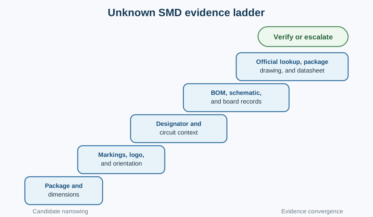
1. Record the Package and Visible Clues
Take a picture of the SMD in full context, including enough of the PCB to associate it with the correct PCB. Record the body shape, termination style, number of pins, dimensions, top marking, logo, orientation feature, revision number of the board, and location of the device. Start with Non-Destructive Inspection (NDI); do not connect power to the device and do not remove it from the PCB until you completely understand the state of the PCB and the intent of your measurement.
Retain the original photograph of the device, reference the scale, and document the units used for the measurement. Examine the surface of the package with oblique light, as it can highlight faint markings that may have been made with a laser. Preserve uncertainty in markings by keeping multiple options for certain letters and numbers, as these may represent different candidates; for example, 0/O, 1/I, or 5/S may represent different possible candidates.
2. Use Board Context to Limit Your Candidate Pool
Use the designator, printed circuit board (PCB) silkscreen, position of surrounding parts, connector positions, power distribution, and expected function of the PCB to limit the candidates based on the available information. If the part is located next to an MCU supply pin, it may indicate that the part is being used as a decoupling capacitor. Conversely, if it is located at the entrance to a connector, it may indicate that the part is used to protect the connector or control electromagnetic interference.
These indications allow you to eliminate candidates that are impossible; however, they do not provide the value, rating, pinout, or installed manufacturer part number (MPN).
The context of where these parts are seen on the PCB may reflect the original design intent, but not necessarily the current condition of the parts. If the PCB has been repaired, or an alternate version of a part has been installed, the silkscreen text may reflect either the original PCB revision or a change that was made without appropriate documentation.
3. Perform a Comparison Against BOM, Schematic, and Official Documentation
To confirm a candidate, collect the BOM, schematic, assembly drawings, purchasing history, mechanical drawings, and datasheet. The reference designator gives the circuit location of the part on the PCB. The value (or comment) gives the intended purpose of the part in the circuit. The footprint identifies the pattern used to mount the part. The manufacturer name, full MPN, and other approved alternatives provide procurement options.
When comparing dimensions, terminal geometry, pin functions, electrical ratings, ordering suffixes, and marking format, a manufacturer lookup will only show the manufacturer’s documented product line. Texas Instruments provides a TI product package marking information lookup tool, but this does not cover every manufacturer.
4. Confirm the Candidate, or Escalate
A candidate is confirmed only if it has compatible packaging, orientation, pin function, electrical requirements, and supporting documentation. The BOM and schematic documents show the original design intent. However, they may not reflect the current state of the parts, such as repairs, approved substitutions, or undocumented revisions.
Confidence levels should be stated according to the degree of confidence. A part may be classified as “probably a capacitor”, an acceptable replacement may be found without identifying the original MPN, or physical evidence combined with design records may confirm the part currently installed. Any discrepancies found between dimensional measurements, pin assignments, polarity, ratings, board history, or other aspects of the candidates require a full review before replacement.
What Can SMD Markings and Package Codes Prove?
SMD marking codes or package codes reduce the number of parts or packages to consider, but they very rarely provide the guaranteed worldwide identity of a part. The vast majority of small bodies have a simple code, typically a manufacturer abbreviation, logo, or production run code. In the case of very small SMD packages, these codes may not contain any marking at all. Furthermore, a single code can represent parts from different manufacturers.
Each marking on the package should be examined in every plausible orientation, and confusion between “0” and “O” or “1” and “I” should be noted. Document any logos separately from the code or short code because they can often be more informative than the short code itself. Additionally, resistor markings apply only to specific documented styles and sizes of resistors (FAQs about Surface Mount Resistors; Surface Mount Resistors Marking), and Murata states that the specification characters of MLCCs do not share a common universal meaning (Individual Specification Code).
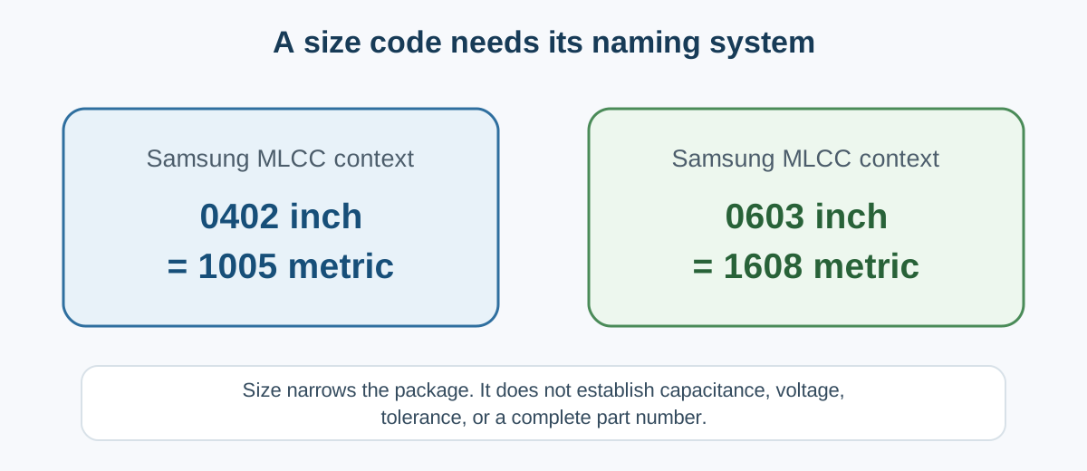
It is essential to name the size system used for capacitors. For example, Samsung’s multilayer ceramic capacitor (MLCC) guide associates the capacitor size 0402 inch with 1005 metric, and 0603 inch with 1608 metric. Other ordering specifications must remain intact because a size code cannot provide a complete capacitor specification (MLCC Product Search).
Using “0402” in a spreadsheet or repair log is not sufficient to inform the reader which measurement system, metric or inch, applies to the capacitor size.
One area where the terminology differs outside component identification is in PCB documents where SMD pads refer to solder-mask-defined pads and NSMD pads refer to non-solder-mask-defined pads. In this context, SMD describes the relationship between the copper land and solder-mask opening, not a component type (TN1224 Mounting Instructions for SMD Packages).
When Should You Stop Guessing and Verify the Part?
When do you know it is time to stop guessing about what you can replace? Stop when multiple candidates visually match the package, the device is damaged or unmarked, a critical pin assignment or rating is unknown, or the installed component is inconsistent with the bill of materials (BOM), schematic, assembly drawing, or board revision. The physical characteristics of the existing component alone cannot justify choosing a replacement.
Stop the replacement decision when unresolved differences could affect electrical compatibility, orientation, thermal behaviour, or board safety. Check the part against the original design or ask for confirmation from the responsible component or repair engineer. Mounting instructions should correspond to the specific package rather than assume that they apply to the generic SMD designation (TN1224 Mounting Instructions for SMD Packages).
Frequently Asked Questions
Q1. What Does SMD Stand for in Electronics?
SMD means surface-mount device. Surface-mount devices are electronic components that connect to PCB pads instead of passing through drilled holes. This abbreviation specifies how an electronic component connects, but it says nothing about the electrical properties of the component.
Q2. Are SMD and SMT the Same Thing?
No. SMD refers to a type of electronic component, while SMT refers to the method used to assemble and attach surface-mount components. Therefore, while the bill of materials may specify an SMD package and manufacturer part number, the assembly plan specifies solder-paste application, placement, reflow, and inspection.
Q3. Do All SMD Components Have Polarity Markings?
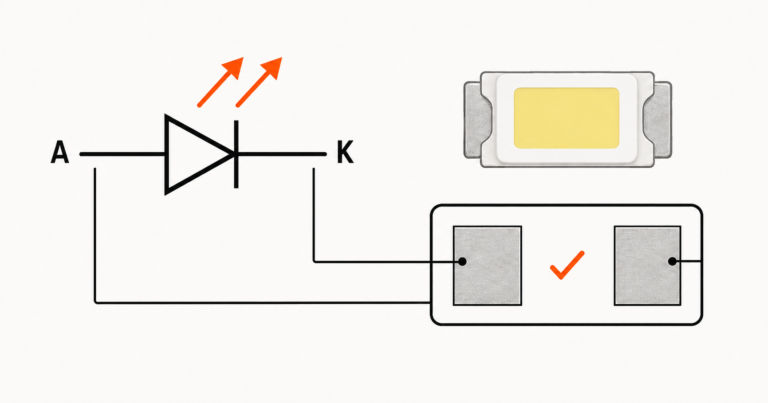
No. Chip resistors and standard MLCCs are not polarized. On the other hand, diodes, polarized capacitors, LEDs, and many ICs require a defined orientation. This may be indicated by a band, dot, notch, symbol, or physical package feature. Three-terminal MLCCs are not polarized, but their through and ground electrodes must be positioned correctly on the PCB. Follow the exact package drawings and datasheets.
Q4. Can SMD Components Be Soldered With a Regular Soldering Iron?
In some cases, yes. Chip capacitors, other two-terminal components, SOT-23 parts, and SOIC packages with accessible terminals may be soldered using a soldering iron, flux, tweezers, magnification, and ESD precautions. Fine-pitch leads require more precise alignment and solder-volume control.
In general, traditional soldering irons are not adequate for QFN, DFN, LGA, BGA, or similar packages with central exposed pads because some joints are beneath the package body. These packages normally require controlled paste application and heating, followed by a package-appropriate inspection method such as X-ray (QFN and SON PCB Attachment).
Q5. Does SMD Always Mean Surface-Mount Device?
Not necessarily. Most electronics and component glossaries define SMD as a surface-mount device. However, in PCB land-pattern documentation, SMD can mean solder-mask-defined, particularly when contrasted with NSMD. The surrounding context determines whether the document refers to a component or pad design.
Conclusion
While the term SMD defines how the component connects to the PCB, it does not define how the component appears, where it may be located on the PCB, or how it functions electrically. Because terminations are the primary visible indicator for inspection, Automated Optical Inspection can verify visible chip terminations or gull-wing leads, whereas underside lands or solder balls may require X-ray inspection or tighter manufacturing process control. Meanwhile, SMT defines the method of placing and soldering surface-mount components rather than a specific connection style.
Visual clues are a useful starting point for component identification, but they do not provide all necessary identification or verification criteria. Always verify that the exact part or replacement component meets the required package dimensions, orientation, electrical requirements, PCB records, and manufacturer documentation. Any discrepancies between these sources must be resolved before changing the PCB.
References & Sources
- SMD — Analog Devices
- FAQs about Surface Mount Resistors — TE Connectivity
- Packaging Part Marking Lookup — Texas Instruments
- Do chip multilayer ceramic capacitors have polarity? — Murata Manufacturing
- Individual Specification Code — Murata Manufacturing
- MLCC Product Search — Samsung Electro-Mechanics
- Surface Mount Resistors Marking — Vishay
- TN1224 Mounting Instructions for SMD Packages — STMicroelectronics