Upload BOM & Gerber

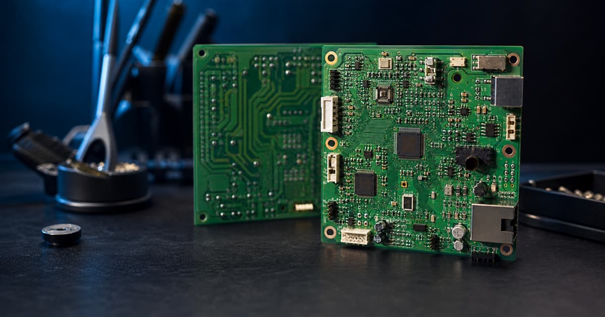
Besides providing mechanical support, a bare PCB creates conductive paths. Alone, it cannot perform the intended electronic function. PCB assembly adds and connects the specified components, and at the end of this stage, the PCBA is ready for the specified inspection and testing stages.
The scopes of work and defined deliverables for PCB design, PCB fabrication, PCB assembly, PCB testing, and box build differ. PCB design creates the board design, PCB fabrication produces the bare board, and PCB assembly places and solders the components onto the bare board. PCB testing and box build describe later work that may be required to complete the finished product.
Key Takeaways
- Assembly creates a populated PCBA.
- Fabrication produces the bare board; placement and soldering belong to assembly.
- Seven stages describe the common flow, but board sides, package geometry, soldering methods, and required test coverage can change the sequence.
- Design and box build remain separate scopes.
Contents
show
What Is PCB Assembly?
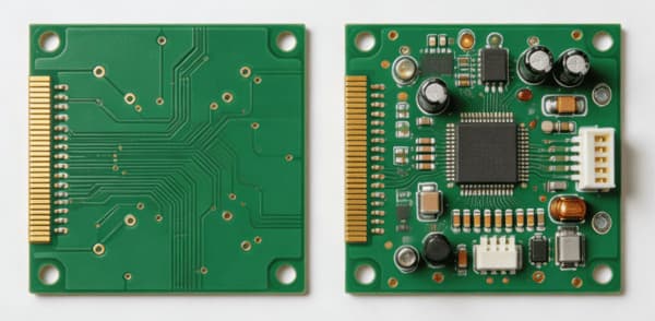
PCB assembly has both a final product definition—the populated PCB, or PCBA—and a process definition, “PCB assembly.” Normally, PCB refers to the bare board, whereas PCBA refers to the populated assembly. Although the populated board is complete at this point, many operations, such as firmware upload, conformal coating application, installation of associated hardware, cables, and labels, and system-level verification, may still need to take place. However, these operations are not required for all PCB assembly projects, and their requirements should be clearly defined in the project scope.
Consider an imaginary motor-drive controller project. The product uses a bare PCB, which contains copper tracks, solder pads, plated holes, solder mask, and component markings. PCB assembly adds the controller, power devices, resistors, capacitors, and connectors and makes solder connections between the components. This completed assembly is now considered a PCBA. A PCBA becomes a finished motor controller after firmware programming, cable installation, enclosure integration, and system testing are completed.
Core Terms Used in Assembly
| Term | Plain-language meaning |
|---|---|
| Fiducial | Optical reference mark used to align machine coordinates with the board |
| Stencil | Thin sheet that deposits solder paste through selected apertures |
| Feeder | Device that presents packaged parts to placement equipment |
| Nozzle | Interchangeable tip that picks up and places a component |
| Reflow | Heating process that melts solder paste and forms SMT joints |
| Tombstoning | Defect in which one end of a small component lifts from its pad |
| Bridging | Unintended solder connection between adjacent conductors |
| Testability | Design features that provide useful electrical measurement access |
PCB, PCBA, and PCB Fabrication: The Key Differences
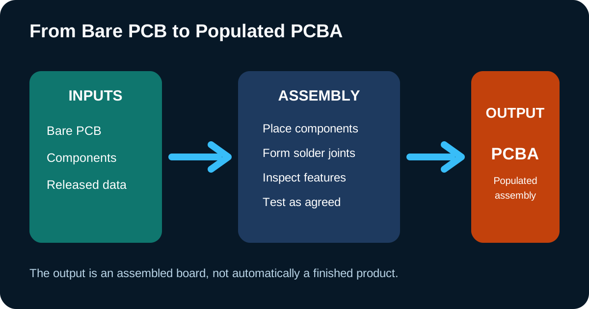
PCB, PCBA, and PCB fabrication are three interrelated terms but differ in meaning. The design phase develops the information needed to manufacture a PCB. The fabrication phase is where the design files are converted into a bare PCB. The assembly phase installs the electrical components onto the PCB. Once the PCB and components are assembled together, the result is a PCBA ready for testing, integration, or product-level work.
| Term | Main work | Output |
|---|---|---|
| PCB design | Create the schematic, layout, and manufacturing outputs | Released design package |
| PCB fabrication | Build the conductive and insulating board structure | Bare PCB |
| PCB assembly | Place, solder, inspect, and test as agreed | PCBA |
| Box build | Add the enclosure, cables, and other system parts | Product or subsystem |
The fabrication stage creates the copper layers and holes and finishes the PCB with solder mask and legends. The assembly stage takes the finished PCB and the component set.
The separation of the terms PCB and PCBA has implications for the ordering process. When ordering PCB units, the manufacturer may supply only bare PCB units. When ordering PCBA units, the request typically includes sourcing or supplying the needed parts, installing and soldering them, and processing the assembly through the specified checks before the PCBA can be delivered. Neither PCB nor PCBA alone fully describes programming, coating, cable assembly, or enclosure work.
What Inputs Are Needed Before PCB Assembly Begins?
The assembly input consists of an assembly data package, and each assembly data package contains different inputs that further define the assembly process. Typical inputs for PCB assemblies include board data, a BOM, placement data, assembly process guidance, and test requirements. KiCad version 9.0 provides documentation for Gerber, pick-and-place, and PDF drawing outputs. Altium provides assembly data documentation defining the position, rotation, and board-side fields of the PCB assembly data sent to the PCB assembly process.
For example:
- Board data: Shows the exact revision of the PCB fabrication files.
- BOM: Indicates the approved manufacturer part numbers as they relate to designators, including all permitted substitutes and intentional no-fit positions.
- Placement data: Contains the information required to place components on a PCB, including component coordinates, rotation, and the side of the board on which each component will be mounted.
- Assembly guidance: Contains the electrical polarity of electronic components, any mechanical limitations, and assembly operations not covered by the placement data.
- Test requirements: Define what must be functionally stimulated or measured, which test fixtures and firmware are used, what pass/fail limits apply, and how the test results will be formatted.
The information in each document, including the BOM, placement data, and drawings, must describe the same build. If the BOM indicates that one part is to be used at R17 while the drawing indicates that another part should be used, the assembler will have questions about which part should be installed at R17. All component packages must match the associated footprints, and component polarity must agree across the files. Additionally, all unpopulated positions on the boards must be clearly identified.
Before the assembly is released for production, the assembler must compare the BOM, placement data, drawings, board revision, approved substitutes, and test plan and verify that they are consistent. A schematic provides electrical information about the circuit; it does not provide a complete assembly data package.
How Does the PCB Assembly Process Work?
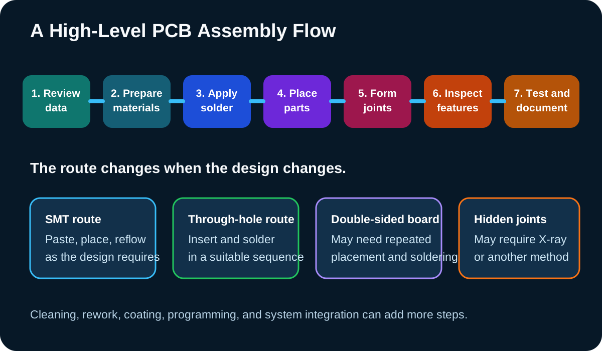
A typical PCB assembly process reviews and verifies assembly data, prepares boards and components, applies solder materials, installs components, forms solder connections, visually inspects assembly quality, and completes the specified functional test requirements. NASA-STD-8739.2 describes comparable preparation, deposition, placement, soldering, cleaning, inspection, and rework activities for NASA hardware.
1. Review the Assembly Data
BOM entries for each component, such as designator, description, footprint, assembly location, and orientation, must match across all documents. The assembler will look for all entries with populated designators and determine what each designator represents. All discrepancies between the BOM, pick-and-place data, drawings, and test documents must be resolved before production.
2. Prepare Boards, Components, and Materials
Preparing each of these items confirms its identity, quantity, packaging and storage conditions, and handling requirements. Parts packaged in reels, trays, tubes, or loose form do not enter an assembly line in the same way. The packaging method must be considered for both manual and automated processes. Tooling and solder materials must also match the selected assembly method.
3. Apply Solder Material
In many SMT assembly processes, a stencil is used to apply solder paste to selected pads on a PCB. Board alignment and support influence the position of the solder paste when it is applied. If SPI is required to verify that the correct amount of solder paste has been applied before components hide the deposits, SPI is conducted before component placement. Other methods include solder wire, solder preforms, wave soldering, and selective soldering, depending on the selected assembly method.
4. Place the Components
Placement equipment uses an X-Y coordinate system, orientation, board-side information, and optical fiducials to place components accurately. When a feeder presents packaged devices to the placement machine, a suitable nozzle picks up each device from the feeder and places it on the assigned footprint. Components such as through-hole components, unique component package types, and some mechanical components will likely require additional or separate processing. Double-sided assemblies require a deliberate sequence to avoid damaging the completed side.
5. Solder the Connections
Solder joints are commonly formed using a reflow oven to heat the solder paste until it melts, wets the compatible metal surfaces of the component, and solidifies around the component terminals as it cools. Components with through-hole terminals may require one of several joining processes, such as wave, selective, or manual soldering. Mixed-technology assemblies will often go through multiple operations; therefore, components must be handled and heated in a way that does not damage previously installed components.
6. Inspect the Assembly
Assembly verification consists of inspecting for defects that the selected inspection method can detect or measure. Different tools are used to evaluate paste position, component presence, polarity, alignment, visible solder contours, and hidden solder connections in a PCBA. Skewing, tombstoning, and solder bridging represent different defects. Inspection visibility is limited by the geometry or physical shape of the components.
7. Test the Agreed Behavior
Testing verifies that specified accessible electrical networks or specified product functions are working as expected. Continuity testing, ICT, and functional testing should not serve as replacements for one another. The test plan must specify coverage, fixtures, programming, limits, pass/fail criteria, and any records that must be maintained during the testing process.
Cleaning, rework, coating, programming, or integration with another product can add stages. The seven-step model outlines the transition between stages without assuming that every PCBA follows a predefined linear sequence.
Surface-Mount, Through-Hole, and Mixed Technology
These three methods classify how component terminals interface with a PCB. SMT places components on pads on the surface of the PCB. Through-hole assembly inserts leads through plated holes in the PCB before soldering. Mixed-technology boards use both SMT and through-hole assembly methods. The design and application determine the appropriate method; neither method is automatically the best choice for every application.
Surface-Mount Technology
SMT combines solder paste printing, component placement, and reflow. NASA-STD-8739.2 defines SMT as a method for component installation on the surface of a PCB.
Through-Hole Assembly
Through-hole assembly is defined as inserting leads through plated holes in the PCB. This construction method can be used for connectors, transformers, switches, and other components when the electrical or mechanical design requires it. However, using through-hole assembly does not necessarily validate the assembly’s reliability. Factors such as hole size, lead fit, PCB and lead materials, soldering conditions, and established acceptance criteria all contribute to assembly reliability.
Mixed Technology Assembly
Mixed-technology assemblies are PCBs that incorporate both SMT and through-hole components. Their assembly plans may separate paste printing, placement, reflow, insertion, and selective or hand soldering. When constructing a mixed-technology assembly plan, component temperature limits, inspection and testing access, component locations on the PCB, and the available equipment determine the sequence of steps.
Who Is Responsible for Design, Fabrication, and Assembly?
The designer provides the design and manufacturing data, including production-ready assembly drawings. The PCB fabricator produces the bare board. The PCB assembler builds the PCBAs from the validated assembly data package received from the designer. A box-build provider combines the PCBAs with cables, enclosures, and other system components to produce a complete system.
| Role | Typical output | Decision to confirm |
|---|---|---|
| PCB designer | Versioned design package | Who may change the circuit, footprint, or approved parts? |
| PCB fabricator | Identified bare boards | Which specification and revision apply? |
| PCBA assembler | Populated assemblies and requested records | Which checks, criteria, and exceptions must be reported? |
| Box-build provider | Integrated product or subsystem | Which firmware, wiring, labeling, and final checks are included? |
While assembly does not include circuit design in and of itself, an engineering service may be provided under a different contract, but there must be an approval process to determine who has final authority over any alternate components or modified outputs. If the assembly data package is not yet ready, it will be necessary to use PCB design services. Final integration of the circuit assembly into the box build or system assembly is usually done afterward.
How Are PCB Assemblies Inspected and Tested?
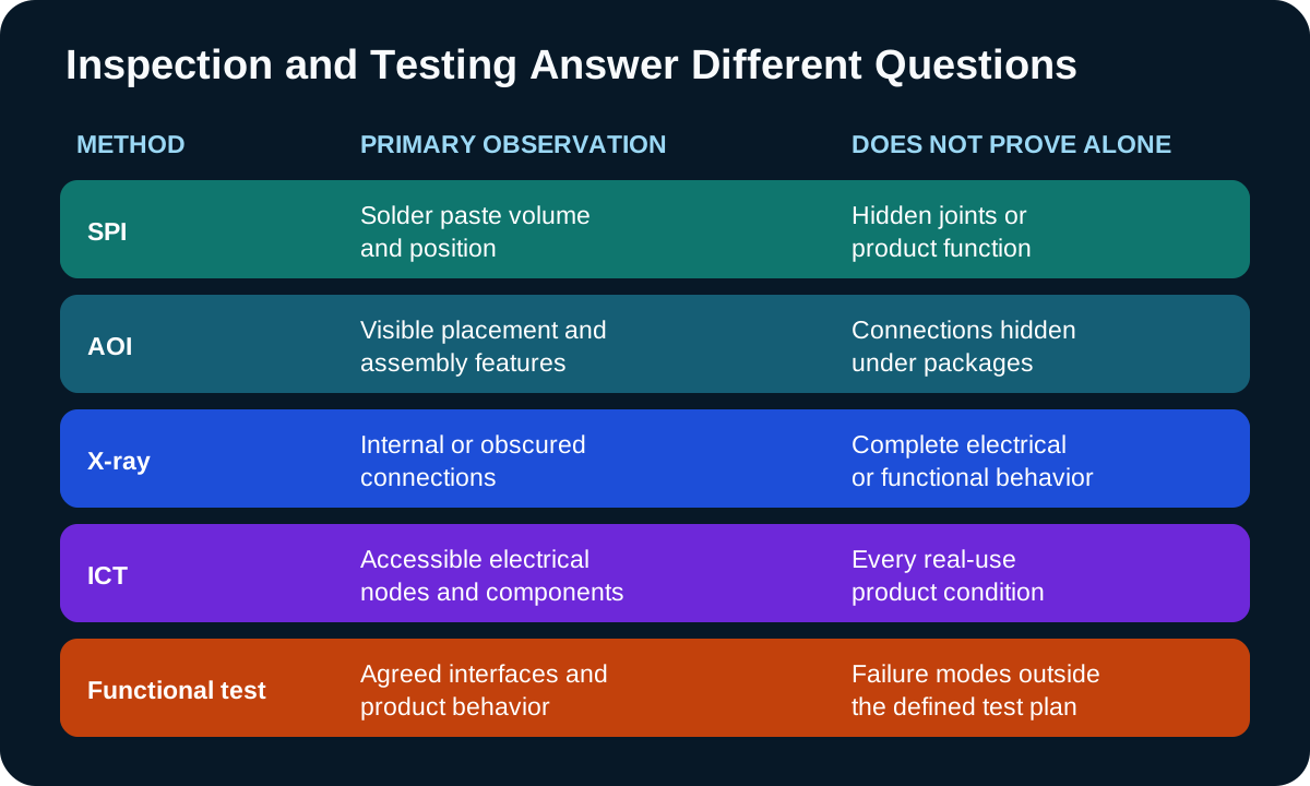
Inspection and testing of PCB assemblies include inspection of physical features and processes and testing of electrical networks or behaviors of the assembled product. SPI evaluates the amount of paste deposited, AOI evaluates visible assembly features, X-ray detects hidden connections, ICT measures accessible points, and functional testing verifies defined behaviors of the product.
SPI inspection is performed prior to placement or reflow while the paste remains visible. AOI can inspect for correct placement and exposed solder features but does not provide a complete inspection of the solder joints under a BGA. X-ray can reveal internal structures but does not verify that the product is fully functional.
ICT applies electrical measurements to the electrical assembly through accessible test points or other possible contact points. Keysight describes several types of defects that can be identified through ICT, such as missing parts, shorts, tombstoned components, lifted leads, solder defects, and incorrect electrical properties. The amount of coverage available with ICT is dependent on several factors, including testability, fixture design, probe access, tolerances, and the test program design. A solder bridge may be detected as an unintended short circuit.
Functional testing requires inputs that are specific to the product being tested. The plan developed for functional testing can include measuring power rails and currents, measuring frequency, measuring digital inputs, measuring indicators and buttons, measuring communications between devices, and other types of responses defined in the test plan. The PCB assembler and the customer must establish parameters such as the jig, firmware, limits, acceptance criteria, and reporting formats prior to commencing production of the PCB assemblies.
The most recent revisions listed in the official IPC document were IPC-A-610 Rev J and J-STD-001 Rev J. IPC modified the J Revision documentation to separate soldering requirements from the description of how to accept assemblies after they have been soldered. IPC documentation does not provide proof of a supplier certification, product class, or test coverage.
The extent of useful test coverage is influenced by factors such as the component package, the available features to be assessed, the risk posed by the product, and the customer’s requirements.
Frequently Asked Questions
Q1. What Is the Difference Between a PCB and a PCBA?
A PCB is the completed or “bare” board that has been manufactured with electrical conductors, holes for solder connections, insulating material, and mechanical support. A PCBA is that same board after the required components have been attached and soldered to the board. If a customer wants to obtain assembled boards, the order must define assembly along with any testing or inspection requirements that must be performed.
Q2. Is PCB Assembly the Same as PCB Manufacturing?
Ambiguity may be caused by the phrase “PCB manufacturing,” which may be interpreted as the entire PCB manufacturing process. PCB manufacturing may refer to fabrication, which is the manufacturing process that creates the bare board. The PCB assembly phase installs and connects the components. An order should provide separate definitions of what is included within each manufacturing phase, as well as what is included in sourcing, programming, testing, coating, and final assembly.
Q3. What Information Does a PCB Assembler Need?
Typically, the assembler will require version-matched board data, a BOM, pick-and-place data, assembly guidance, and test specifications. An assembly data package identifying the approved parts, intentional no-fit locations, orientation, permitted component substitutions, and board revision must be provided. All files must describe the same assembly configuration.
Q4. Does a PCB Assembly Company Design the Circuit?
Engineering support is not inherently included within PCB assembly.
Typically, PCB assemblers perform their work based on approved manufacturing and design data. Some PCB assemblers provide engineering support as a separate service. The circuit change document should state who can change the circuit, footprint, BOM, or outputs and who approves any replacement parts prior to continuing production.
Q5. Are All Assembled Boards Functionally Tested?
Not every assembled board is functionally tested. The extent of electrical test coverage is based on the product, interfaces, test fixtures, firmware, risk, production volume, and customer requirements. Some PCB assemblies include inspection and electrical testing; other assemblies also include ICT, programming, and functional testing. Ask for details about the electrical testing, how the results will be compared against the pass limits, and what must be stimulated, measured, recorded, and compared.
What Should You Remember About PCB Assembly?
PCB assembly changes a bare or unpopulated board into a populated PCBA. PCB assembly does not automatically include circuit design, original bare-board fabrication, firmware, every inspection process, unlimited functional testing, or final assembly.
Once the documentation is completed, ensure that the same revision is found in each document. Separate fabrication, component assembly, programming, inspection, testing, coating, and final assembly into separate sections or categories. Testing requirements, measuring and recording devices, and comparison against pass limits should be based on component package geometry, accessible features, product risk, and the intended application as determined by the customer.
References & Sources
- NASA-STD-8739.3 — NASA
- NASA-STD-8739.2 — NASA
- KiCad 9.0 Documentation — KiCad
- Preparing Assembly Data for Manufacture — Altium
- Automated Inspection Systems — Omron Automation
- Automated Optical Inspection Technology — Nordson Test & Inspection
- What Is In-Circuit Test? — Keysight
- IPC Document Revision Table — IPC
- IPC Releases J Revisions of Two Leading Standards for Electronics Assembly — IPC
- Inside the Professional PCB Assembly Process at a Leading Chinese Company — SatisFactory Process