Upload BOM & Gerber
-
Mobile: +86 13312967631
-
Email: sales@sugaintl.com

Micro-BGA Assembly and 01005 SMT Assembly
PCB Assembly for Micro-BGA with 01005 Components
Hidden-array packages and 01005 passives require different land, stencil, placement, reflow, and inspection conditions. SUGA assigns each process window according to the actual joint geometry.
SPI, placement, reflow-profile, X-ray, electrical-test, and rework records remain linked to the board and assembly lot.
0.20 mm
Micro-BGA / WLCSP minimum ball pitch
0.4 × 0.2 mm
01005 nominal body size
Cpk >1.33
01005 printing at AR >0.52
What Are Micro-BGA and 01005 Components?
A micro-BGA uses a high-density solder ball or bump array that places the solder joints underneath the package. A micro-BGA might be labeled as FBGA, CSP, WLCSP, DSBGA, or by a supplier-specific package code. An 01005 is a resistor or capacitor with a nominal size of 0.4 × 0.2 mm and is also referred to as 0402 metric. Ball pitch and chip-body dimensions do not represent the same thing. The package name is not enough to identify the package for production; a manufacturer part number confirms the ball diameter, array map, package thickness, warpage limit, MSL, and reflow exposure.
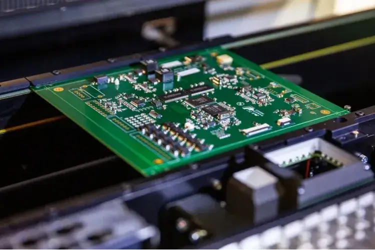
Package and Joint Control Comparison
| Engineering variable | Micro-BGA / FBGA / WLCSP condition | 01005 condition | Process control |
|---|---|---|---|
| Package definition | Supplier-defined ball or bump array | Two-terminal resistor or capacitor; 01005 imperial / 0402 metric | Part number controls land, stencil, placement, and inspection setup |
| Joint visibility | Hidden under-package interconnects | Externally visible end terminations | X-ray/AXI/µCT for arrays; AOI/microscope for 01005 |
| Geometry scale | 0.20 mm minimum BGA ball pitch | 0.4 × 0.2 mm nominal body | Control pitch and body dimensions as separate variables |
| Required component data | Body, pitch, ball diameter, array map, pad recommendation, warpage, MSL, reflow limit | Body tolerance, termination width, component type, recommended land | Define the manufacturing window from the supplier drawing |
| Placement controls | Array alignment, coplanarity, warpage, Z-height, thermal mass | Pickup stability, programmed offset, Z-height, downward force | Match vision library, nozzle contact, feeder presentation, and support-pin layout to the actual package |
| Inspection signals | Bridge, missing/shifted ball, void pattern, head-in-pillow, non-wet-open | Tombstoning, skew, visible bridge, wetting, body damage | Correlate array-location imaging with open/short and functional results |
| Rework constraints | Local heat, site integrity, adjacent hidden joints, prior heat cycles | Small-body handling, termination condition, local access | Record target-site and adjacent-component thermal exposure before structural and electrical release |
Package-Specific Micro-BGA Assembly
Micro-BGA is an industry description rather than a fixed specification for individual packages. Arrays can be available in pitches of 0.20, 0.30, 0.35, or 0.40 mm, with different ball diameters, maps, body sizes, thicknesses, and materials. IPC-7095E is the guiding document for BGA design and assembly implementation, while IPC-7352 provides general land-pattern guidance; however, the specific package drawing is considered the primary authoritative document. The manufacturer part number, package code, ball map, pin-1, placement side, and centroid/XY orientation must all match before program release. A mismatch could cause the correct package to be assembled in an incorrect orientation, map an X-ray call to the wrong ball location, or release the program with an incorrect centroid.
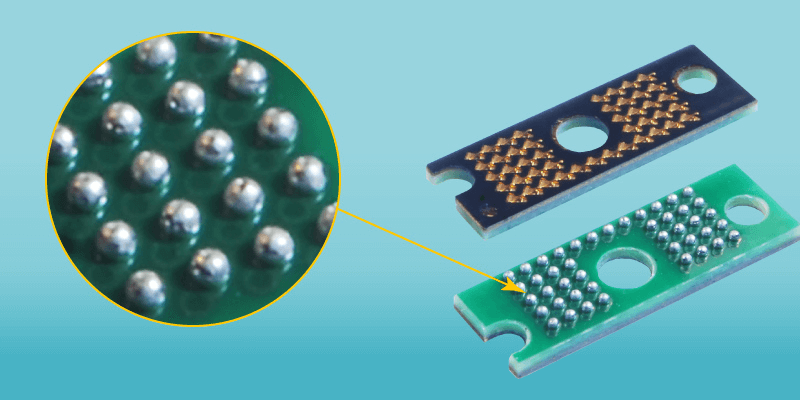
Package recognition involves knowing the physical geometry of both the package body and ball array, along with fiducial correction, nozzle selection, pickup height, and board support. Hidden interconnects make the assembly process focus on alignment, coplanarity, warpage, and under-package inspection. X-ray coverage is planned from the array map and surrounding copper or via structures instead of from the visible package perimeter.
01005 Dimensions Compared with 0201
The nominal body for the 01005 case is 0.4 × 0.2 mm, compared with 0.6 × 0.3 mm for the 0201 case. The actual length, width, height, and termination tolerances come from the part drawing for the selected component.
The range of 01005 capacitors is from 0.38–0.42 × 0.18–0.22 mm, with termination widths ranging from 0.07 to 0.14 mm. A resistor example is specified as 0.40 ± 0.02 × 0.20 ± 0.02 mm. Capacitor and resistor terminations therefore require separate lands, paste deposits, and mechanical controls.
Two different parts carrying the same 01005 size code may still have different termination widths, body heights, construction methods, reel presentations, and manufacturer land recommendations. These differences will result in varying solder volumes, nozzle contact, board-flex loads, and tombstoning responses.
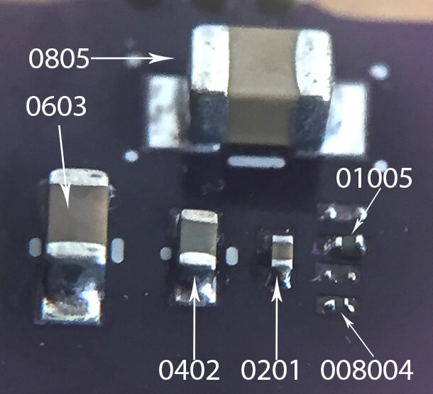
01005 Land Pattern and Spacing
The land pattern for an 01005 component starts with the specific part number used for the resistor or capacitor. SUGA combines the body and termination dimensions with the manufacturer land recommendation, surface finish, solder mask, component orientation, board mechanics, and component density on the PCB.
01005 Land and Clearance Control
| Design variable | Qualified data / condition | Manufacturing control |
|---|---|---|
| Component drawing | Body, termination, tolerance, manufacturer land recommendation | Use selected part number as footprint input |
| Capacitor land | Manufacturer-labelled A/B/C: 0.15–0.25 mm each | Balance solder volume, mask, finish, mechanics, orientation |
| Resistor land | Body 0.40 ± 0.02 × 0.20 ± 0.02 mm; a=0.15 mm, b=0.20 mm, l=0.20 mm | Apply resistor land plus reel/termination data |
| Capacitor DOE | 210 × 220 μm pads; 160 μm separation | Print and placement comparison |
| Resistor DOE | 190 × 220 μm pads; 160 μm separation | Independent resistor comparison |
| Adjacent copper | 100 μm separation; no bridging under tested conditions | Coordinate copper, mask, paste, orientation, neighboring body |
| Body clearance | 7 mil = 177.8 μm | Set after layer, mask, paste, orientation, placement-nozzle access, and inspection view are fixed |
| Solder-mask web | Registration, mask process, copper geometry, board class | Select mask-defined or non-mask-defined treatment |
| Stencil web | 4 mil = 101.6 μm between laser-cut features | Control metal remaining between apertures |
| Courtyard / rework access | Body size, neighboring height, nozzle access, X-ray access, service strategy | Reserve placement, inspection, and local repair space |
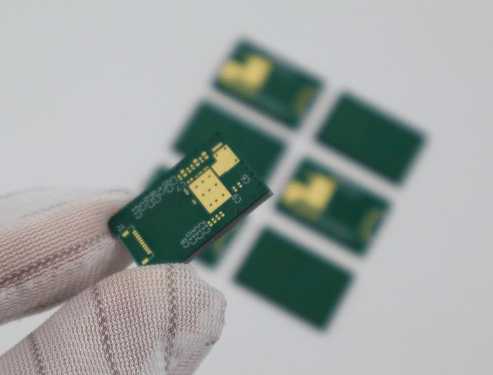
01005 Capacitor Land Pattern
The land patterns for 01005 capacitors should consider potential damage caused by board bending near depaneling lines, stiff connectors, or mounting features. SUGA checks the orientation of the components relative to panel break lines or high-stiffness features and verifies the wetting and body condition of the first article. An MLCC may pass AOI after reflow but crack later during depaneling, connector insertion, screw fastening, or enclosure assembly, so land selection also accounts for mechanical loading.
01005 Resistor Land Pattern
The solder volume at both ends of an 01005 resistor must be equivalent to control skew and tombstoning. Pad geometry, component height, nozzle contact, and board support will affect how the body is loaded.
Even if the centroid is stable, it will not prevent damage to the component body when pocket presentation, pickup height, nozzle overtravel, or local PCB deflection changes. Pickup stability, programmed offset, placement force, and Z-height must all be checked with the selected tape-and-reel and the actual panel-support conditions. SUGA maintains separate footprints for resistors and capacitors even when they use the same 01005 size code.
How Are 01005 Clearances Defined?
Adjacent-copper separation, component-body clearance, and stencil web width describe three different physical objects. Copper and solder-mask registration govern PCB fabrication, body clearance governs placement and inspection access, and stencil web width governs aperture manufacturability. They should not be combined into one generic minimum-spacing rule.
Solder Paste Control Through Stencil Design
A stencil micro-aperture will fail when solder paste cannot fill, release, or coalesce consistently. SUGA evaluates aperture geometry, foil fabrication, foil thickness, paste powder class, gasket contact, and deposit-height requirements as one print condition. The SUGA printing process uses SPI distribution rather than a single deposit measurement to approve printing.
Micro-Aperture Print Window
| Print variable | Qualified window | Process control | Acceptance signal |
|---|---|---|---|
| Aperture geometry | Circle, oval, corner-rounded, oversized circle, square, home-plate, radiused home-plate | Match shape/orientation to land and release direction | SPI volume, height, area, and offset within the qualified limits |
| Stencil fabrication | Laser-cut, electroformed, enhanced/treated laser-cut | Select wall finish by feature size and production volume | Transfer efficiency improved from ~65% to >85% between the tested stencil-fabrication conditions |
| Foil thickness | 75, 76, 80 μm; 0.002 in = 50.8 μm; 0.004 in = 101.6 μm | Match foil to aperture area and component mix | Deposit height meets the Micro-BGA and 01005 joint requirement |
| Area-ratio examples | AR 0.47 with 0.004 in foil; AR 0.98 with 0.002 in foil | Maintain Aa/Aw for the qualified aperture geometry | Stable transfer efficiency with lower deposit variation |
| 01005 print window | AR >0.52: Cpk >1.33; AR >0.60: Cpk >2.00; optimum print response at AR ≥0.59 | Set from SPI distribution and coalescence data | Cpk thresholds met at the stated area-ratio conditions |
| Type 3 paste | Higher defect response in coarse-powder combinations | Restrict to compatible apertures and qualified programs | No incomplete fill, clogged aperture, or unstable transfer trend |
| Type 4 paste | 20–38 μm particle range | Fine-feature route with compatible alloy/aperture | Stable SPI distribution and complete post-reflow coalescence |
| Type 5 paste | At 75 μm foil, transfer close to Type 4 | Smaller apertures or tighter release conditions | Smaller apertures maintain acceptable transfer and coalescence |
| Type 6 paste | 01005-capable ultra-fine powder systems | Ultra-fine or selected low-temperature route | Complete coalescence without isolated solder particles |
| Fine-feature aperture | Repeatable coalescence at 170 μm circle/square apertures | Match paste, aperture finish, alloy, and reflow | Complete deposit coalescence |
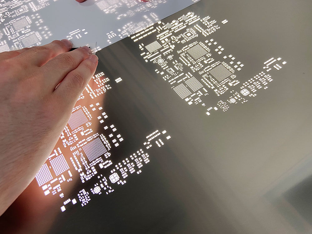
Aperture Geometry for Paste Transfer
When transferring paste through an aperture, the aperture shape, wall finish, gasket contact, separation speed, orientation, and paste rheology all influence how well the paste fills and releases from the aperture.
What Area Ratio Supports 01005 Printing?
For printing 01005 components, the stencil area ratio is determined by taking the area of the aperture openings and dividing it by the area of the aperture walls, or Aa/Aw. Foil thickness must also be taken into account together with the area ratio, as the same board can contain small deposits for 01005 components and larger deposits for connectors, shields, or high-thermal-mass components. If one foil cannot accommodate both types of deposits, aperture modification, stepped thickness, direct flux, or a different deposition method may be needed for that component.
Solder Paste for Micro-Apertures
The selection of the powder class is based on many factors, including aperture size and wall finish, as well as alloy, flux chemistry, print environment, and reflow atmosphere. Once the solder paste has been selected based on the above criteria, other factors such as storage time, thawing and mixing before use, exposure, and subsequent oxidation must be taken into consideration to determine compatibility. The 5-ball rule screens powder-to-aperture compatibility, while SPI distribution and coalescence following reflow help determine whether the combination is viable for production.
Direct Flux for Mixed-Height Printing
A mixed-height assembly placed a 2.7 × 2.4 mm Micro-BGA beside a 26 × 20 mm reader. The Micro-BGA had a recommended deposit height of about 0.08 mm, while the larger package had a recommended deposit height of 0.125 mm. A stepped stencil was used, which resulted in approximately 25% shorted Micro-BGAs. The shorts had nothing to do with package placement but resulted from discrepancies in the solder volumes needed to create reliable joints for the two components.
The qualified first pass used the solder already deposited on the Micro-BGA balls. The placement machine dipped the Micro-BGAs into flux at depths of 0.10 mm and 0.14 mm over 2 panels, resulting in 16 fluxed Micro-BGAs. The results were verified through X-ray and transverse and longitudinal cross-sections.
Documentation for the assembly lot included flux depth, coverage, contamination control, placement alignment, and the recorded reflow profile. If reducing the Micro-BGA stencil deposit would compromise the larger component joint, direct flux would be used for the Micro-BGA because increasing the local paste volume would increase the risk of Micro-BGA bridging.
Placement Accuracy and Reflow Control
Placement and Reflow Process Window
| Process variable | Qualified data | Control inputs |
|---|---|---|
| Equipment position | ±30 μm @ 3σ | Fiducial correction, recognition, first-article measurement, offset data, Cpk |
| Programmed offset | 0.001–0.003 in = 25.4–76.2 μm; 16 boards × 165 placements | X/Y offset versus paste and foil interaction |
| Misalignment classification | 50–100 μm inspection condition | Component, land, paste, orientation |
| Placement force | 3.5 N caused resistor cracking; 1 N lower-force setting | Z-height, overtravel, thickness, speed, force, PCB support |
| SAC reflow | Ramp 1.25 or 1.5 °C/s; peak 240–245 °C; TAL ~60 s | Board-specific measured profile |
| Reflow atmosphere | Air or nitrogen | Wetting, oxidation, voiding, material, product requirement |
| Low-temperature reflow | Melt 146 °C; peak 175 °C; TAL 100–120 s; ramp 1–3 °C/s; Type 4/5/6 | Qualified alloy, component compatibility, reliability requirements, and warpage-sensitive assembly condition |
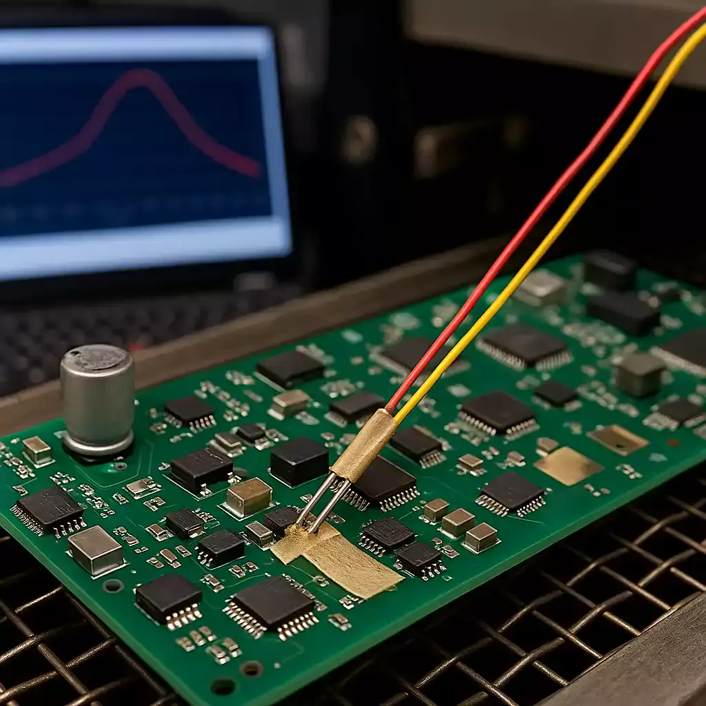
| Thermal-profile baseline | IPC-7530B; component moisture/reflow specification; paste TDS | Thermocouple locations, board setup, oven settings, ramp, TAL, peak, cooling, and retained profile record |
How Is Placement Offset Controlled?
Equipment-position capability and final component-on-pad accuracy are different characteristics. When there is an offset, SUGA separates board-fiducial error, feeder presentation, recognition repeatability, programmed coordinates, paste offset, and stencil interaction before changing the placement program. This separation helps prevent a paste-print shift from being erroneously corrected as a machine-coordinate error. QA verifies the equipment capability of ±30 μm @ 3σ for packages through fiducial compensation and first-article measurement. Programmed offset, observed position, and Cpk values are calculated separately to correct recognition instability before reflow.
How Does Board Support Protect 01005?
Even with the correct placement coordinate, an 01005 body could still crack if the PCB deflects at the point of contact with the nozzle. Z-height, overtravel, downward force, placement speed, component thickness, and support-pin location must be verified on the actual panel. The support pins are located beneath the populated area and do not contact bottom-side features. They are positioned considering panel rails, cutouts, bottom-side components, and local copper stiffness. FAI verifies pickup stability, board deflection, and body condition, while the placement program controls the contact force at each panel location.
Reflow Profiles for Mixed Thermal Mass
A reflow profile developed to meet the Micro-BGA peak temperature may overheat an adjacent low-thermal-mass package or underheat an area of heavy copper. Thermocouples must be placed at the hidden-array package, the dense 01005 area, the heavy-copper area, and the thermally dominant component so that the oven settings are based on the entire board and not just a single location. Air or nitrogen is selected based on wetting, oxidation, voiding, alloy, and product requirements. IPC-7530B is a guide for reflow-profile development, while component moisture and reflow specifications, solder-paste technical data, and IPC J-STD-001J are used to establish soldering process controls. Low-temperature reflow is used for heat-sensitive materials, warpage-sensitive packages, or assemblies with limits on the number of thermal cycles. The alloy, component compatibility, and product reliability requirements establish a separate process from the SAC profile.
Inspection for Visible and Hidden Solder Joints
Inspection Coverage by Joint Visibility
| Inspection method | Inspection target | Defect / signal set |
|---|---|---|
| 3D SPI | 01005 and Micro-BGA paste deposits | Volume, height, area, variance, transfer efficiency, offset |
| AOI | 01005 body and visible terminations | Presence, position, tombstoning, skew, bridge, termination condition, and body damage |
| Microscope | Small or disputed visible features | Wetting, solder shape, contamination, body crack/chip |
| 2D X-ray | Hidden Micro-BGA/FBGA/WLCSP array | Bridge, missing/shifted ball, alignment, gross void pattern |
| Oblique X-ray / AXI | Edge-ball and location-specific patterns | Bridge, alignment, edge-ball anomaly |
| 3D X-ray / µCT | Dense or overlapping structures | Internal geometry, void distribution, package/board interface |
| Cross-section | Qualification or failure-analysis joint | Internal wetting, intermetallic geometry, crack, separation |
| ICT / FCT / ATE | Electrical network and product function | Opens, shorts, circuit response, functional limits |
| Quality record | Board identity plus print, optical, X-ray, profile, electrical, acceptance data | Traceable inspection and test results |
SPI Before Placement
SPI trends help determine whether an anomaly in a single printed deposit is due to progressive contamination of the aperture, degradation of the stencil wall, loss of gasket contact, cleaning-interval drift, or printer offset.
Operators perform corrective actions on the print process and remeasure the printed deposit before components enter placement. The first-article results and production trends associated with those components are linked to the stencil program, paste lot, printer settings, and cleaning response.
Optical Inspection for 01005
The AOI recipe for 01005 is established based on known-good 01005 placements and confirmed defect samples. Because of the very small size of the 01005 component and the resulting body contrast and solder reflections, the potential for false calls at this size must be considered. All threshold changes to the AOI recipes are evaluated against tombstoning, skew, termination wetting, body damage, and placement-position data rather than only to reduce alarm volume.
Confirmed calls are recorded by defect type so that solder imbalance, placement position, body loading, and reflow response can be correlated with the upstream process. Optical acceptance follows IPC-A-610J and the applicable customer class. Soldering materials and process controls follow IPC J-STD-001J.
How Are Hidden BGA Joints Verified?
A top-down view of the components is not sufficient to verify that a joint in a BGA is connected. However, a clean 2D X-ray image may still miss a non-wet-open or head-in-pillow condition. The array position, oblique or three-dimensional imaging, reflow history, and electrical results are correlated before release. SUGA links the print, optical, X-ray, profile, electrical, and acceptance results to the board identity under IPC-7095E, IPC-A-610J, IPC J-STD-001J, and the customer control plan.
Thermal Control During Micro-BGA Rework
Factors considered include underfill, pad and laminate condition, MSL history, previous heat cycles, adjacent-component exposure, and local access for the rework.
Micro-BGA Rework Control Record
| Rework operation | Control inputs | Recorded data | Acceptance output |
|---|---|---|---|
| Pre-rework assessment | Package drawing, MSL/bake, alloy, underfill, board thickness/copper, access, adjacent parts, prior cycles | Component and board history | Approved removal route, bake condition, and allowable additional heat cycle |
| Component removal | Bottom preheat, localized top nozzle, vacuum pickup, measured joint response | Package, PCB, adjacent thermocouples | Package removed after measured solder release without pad lift or laminate damage |
| Site preparation | Residual solder removal, cleaning, pad/mask/via/laminate inspection, coplanarity | Microscope; X-ray/µCT where required | Intact, clean, coplanar site |
| Replacement preparation | Component identity, ball/reball status, flux/paste method, orientation, MSL handling | Incoming and preparation record | Correct part, orientation, ball/reball condition, flux or paste method, and MSL status |
| Replacement placement | Vision alignment, package nozzle, Z-height, PCB support | Placement and first-article results | Pin-1 and array position verified before local reflow |
| Local thermal profile | Bottom/top heat, ramp, TAL, peak, cooling, adjacent thermocouples | Reworked uBGA joint 232.9 °C; adjacent uBGA joint 245.5 °C; CBGA joints 223.0 °C, 218.7 °C, and 211.3 °C; bottom-PCB readings 237.2 °C, 237.3 °C, and 245.1 °C | Target, PCB, and adjacent thermocouples remain within the approved profile |
| Adjacent-component control | Shielding, nozzle selection, thermal separation | uBGA, CBGA, and PCB temperature map | No uncontrolled secondary reflow or adjacent-package damage |
| Post-rework inspection | X-ray/AXI or µCT; microscope at site perimeter | Joint structure and site record | No bridge, missing ball, package shift, pad damage, or unresolved internal anomaly |
| Electrical / functional test | ICT/FCT/ATE or product-specific test | Test result linked to rework record | Required ICT, FCT, ATE, or product-specific test passed |
| Final disposition | Site integrity, thermal window, prior cycles, adjacent exposure, test coverage | Engineering decision | Rework, replacement, or scrap |
Component Removal and Site Preparation
The target joints are brought to the intended reflow temperature through bottom preheating and localized heating from a top nozzle before vacuum removal of the part. Next, residual solder and flux are removed from the area, allowing inspection of the pads, mask, vias, laminate, and coplanarity before replacing the part.
Before replacing the component, all inspection findings and site conditions must be documented, including lifted pads, damaged mask material, damaged laminate, contaminated pads, local warpage, and the condition of the pads and mask. Only a flat, clean, intact, and coplanar site proceeds to replacement under the applicable component moisture requirements.
Local Thermal Control During Replacement
The measurements show that localized heat from the rework process can extend beyond the area where the part was installed. Adjacent packages and the bottom side of the PCB can experience heating at or above the target-site temperature; therefore, nozzle geometry, shielding, bottom heat, and thermocouple locations must be adjusted according to actual thermal-coupling measurements rather than relying solely on station settings.
Post-Rework Acceptance
After rework, acceptance of the reworked area is based on site integrity, hidden-joint structure, and the applicable electrical or functional result. These items must be reviewed against the original defect findings and rework profile to ensure that an image pass does not mask an unresolved circuit failure and that an electrical pass does not close an unexplained structural anomaly.
The rework documentation includes board identification, component and lot identification, operator name, the program used to perform the rework, the measured rework profile, prior heat cycles, inspection records for the replacement component, and the final condition of the reworked site in accordance with IPC-7711/21D, IPC-A-610J, IPC J-STD-001J, and IPC-7095E.
Applications for Micro-BGA with 01005 Components
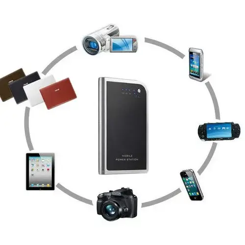
Handheld Consumer Electronics
Micro-BGA and WLCSP packages support processors, memory, cameras, power management, and control devices in compact handheld layouts. 01005 components also provide decoupling, filtering, and compact power delivery around shields, cameras, and connectors. The primary risks in a handheld unit are local board deflection and thermal shadowing at shields, camera connectors, and thin PCB areas. Support-pin placement and reflow profiling consider secondary shield attachment and connector thermal mass, allowing the Micro-BGA to maintain coplanarity without increasing the risk of 01005 tombstoning.

Wearable Electronics
TWS devices place 01005 components close to sensors, battery management, wireless communication, audio, and power circuits, while Micro-BGA or WLCSP packages contain the controller, codec, or radio functions. Rigid, flex, and rigid-flex boards require stable pickup, controlled support, low package height, optical inspection, hidden-array imaging, and product function checks. Components near a rigid-flex transition, enclosure contact point, battery support, or repeated-bend region may pass assembly inspection while failing under mechanical loading. The evaluation covers bend-line distance, populated-flex support, package height, enclosure pressure, mechanical bending, and depaneling stress.

Portable Medical Electronics
Compact medical sensors use 01005 components for low-power filtering, sensor front-end circuits, and dense power networks. Micro-BGA or WLCSP packages provide processing, wireless communication, or control functions in portable medical devices. Low-level sensor or analog front-end circuits can be affected by flux residue, ionic contamination, leakage paths, or incomplete cleaning even when the solder joints appear acceptable. Requirements for product cleanliness, process chemistry, test limits, moisture handling, SPI, X-ray/µCT, and lot traceability remain tied to the same assembly record.
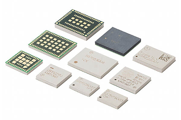
Wireless SiP Modules
01005 components form RF matching, decoupling, filtering, and power nodes on the wireless SiP. Micro-BGA, SiP, and WLCSP packages support radio control, baseband, memory, and digital interconnect functions. If one 01005 matching component is shifted or the solder volume on one side is unequal, the effective parasitics may not match the expected values even though the component remains electrically connected. Shield proximity may affect the AOI or X-ray angles. SPI and placement data must therefore be analyzed with RF or frequency-specific functional results instead of being released based only on optical placement.
IoT Edge Devices
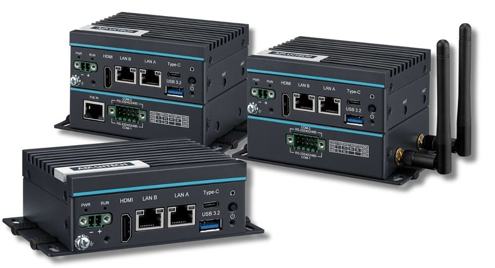
IoT edge boards use 01005 components across sensing, wireless communications, power, and security zones. Micro-BGA or WLCSP packages support processor, communication-controller, or secure-element functions. The primary risk with an IoT edge device is confusing an assembly defect with an approved BOM, a DNP part, firmware versions, or regional radio variants. Board identity, component population, programmed configuration, inspection results, and functional-test limits are mapped to the same serialized unit to differentiate between physical defects and approved product variants.
Processors and Memory Systems
Micro-BGA and FBGA packages are packaging solutions for high-speed processors, controllers, and memory devices with a high density of I/O. Very small passives such as 01005 components are used with high-speed devices to provide high-frequency decoupling, power filtering, and signal conditioning immediately adjacent to the package. The use of via-in-pad structures, dense power planes, package warpage, and mixed thermal mass can lead to edge-ball irregularities or head-in-pillow conditions without an obvious top-side placement error. X-ray images of the array area, measured profiles, power-test results, and functional-test results are reviewed together, especially after rework near another processor or memory package.
Our PCBA Production Lines
















Micro-BGA and 01005 Frequently Asked Questions
Yes. However, the two types of components on the same PCB do not share the same land, paste volume, placement force, or inspection conditions. Paste volume is managed through SPI, while visible 01005 joints are inspected using AOI or microscopy, and the hidden array of solder joints is inspected using X-ray or AXI.
Micro-BGA has a much smaller ball pitch or ball geometry than many standard BGA packages. This leads to less tolerance for variation in the land, paste transfer, placement offset, package warpage, and thermal imbalance. The tighter requirements of Micro-BGA packaging drive the need for tighter print and placement tolerances and require array-specific X-ray inspection of hidden joints, together with correlation with electrical test results.
The complete input file set for Micro-Assembly should include the following: BOM with manufacturer part numbers; PCB fabrication data; centroid/XY data; assembly and package drawings; ODB++ or Gerber data; orientation; panel details; approved alternates; MSL requirements; quality class; and test plan.
Ask the supplier which alloy and paste combination the air-versus-nitrogen qualification was based on and whether it was tested against your board’s thermal mass mix. A nitrogen recommendation from one product profile will not necessarily transfer to a board with a different mixed thermal mass.
Micro-BGA and WLCSP packages are handled according to their specified MSL, floor life, dry-pack condition, humidity-card result, and bake requirements. SUGA tracks labels, lot number, opening time, storage conditions, and prior rework heat cycles. Sealed packaging or dry-cabinet storage is used as required.
Yes; however, this is only valid if the site has sufficient access to perform the rework and the pad, solder mask, neighboring components, and previous heat exposure remain suitable for localized replacement. SUGA controls handling, heat input, cleanliness, and optical inspection and identifies the applicable electrical test requirements after rework.
Please refer to the quality record row in the inspection table and the rework record above for what is captured by default. Confirm when placing an order which records are retained and shared as standard and which are produced only on request. Supplier retention periods for X-ray images and SPI trend data may be shorter than required for later field-return investigations.