Upload BOM & Gerber
-
Mobile: +86 13312967631
-
Email: sales@sugaintl.com

PCB Electrical Testing
Netlist-Based Testing Before PCB Assembly
Match the approved board revision to the electrical test program, then test intended connections and required separation before components are installed.
100% Bare-PCB Electrical Test
Continuity Threshold ≤0.1 Ω
CAD-to-Fabrication Netlist Comparison
PCB Electrical Testing Fundamentals
PCB electrical testing validates that the manufactured PCB matches the approved connectivity before use. Three areas of interest for electrical testing are whether intended paths remain electrically continuous, whether nets that need to remain separated are still electrically isolated, and whether the electrical test result can be traced back to the exact board, program, and revision tested.
SUGA performs electrical testing on every bare PCB manufactured. A continuity threshold of less than or equal to 0.1 ohm is available when specified, and electrical connectivity derived from CAD files is checked against connectivity derived from fabrication data when both controlled data sets are supplied. The report specifies the actual program settings, accessible nets or points, number of nets excluded from testing, and the board revision.
| Test objective | Failure signature | Measured evidence | Pass condition |
|---|---|---|---|
| Intended connection | Open / broken trace / discontinuous plated path | Continuity at mapped locations | Path resistance meets programmed threshold |
| Required separation | Short / copper bridge / adjacency fault | Isolation between named nets | Isolation meets programmed criterion |
| Completed program | No confirmed open or short in tested range | Board-linked result with nets, settings, and coverage | Bare PCB accepted for recorded program |
Continuity Testing for Open Circuits
Continuity testing uses electrical measurements for each programmed net and corresponding path on the PCB, measured through pads, traces, and plated connections. When the resistance measurement is higher than the specified limit, the affected net and contact points can be identified, allowing engineering to perform a localized investigation into the cause of the discontinuity without assuming a general failure of the entire board.
The via measurement verifies electrical conduction through the plated connection under the settings used during testing. This test does not confirm hole-wall thickness, plating integrity through thermal cycling, or defect-free performance over the life of the PCB.

Isolation Testing for Short Circuits
Isolation testing determines whether separate nets remain electrically isolated under the programmed test conditions. A connection between nets that must remain separate indicates a copper bridge, adjacency fault, conductive residue, or another unintended conductive path. The affected electrical relationship can be traced to the corresponding contact locations on the board for confirmation.
The isolation criterion determines whether the measured separation passes, while the applied voltage records the condition under which the evaluation was completed. Both values remain part of the result so that a short or leakage indication is not separated from its test condition.
Limits of a Passing Electrical Test
Bare-board E-test determines the electrical relationships of circuit paths before components are placed. Unless separately specified, bare-board testing does not provide assurance of hole-wall construction, controlled impedance, dielectric withstand, thermal or flex life, component behavior, calibration, or assembled-product function.
Bare-Board Electrical Test Process
The bare PCB electrical testing process is a controlled sequence that uses the correct board data to generate a test program. The test process establishes repeatable contact for continuity and isolation measurements and associates the test results with the board or panel being tested.
- Controlled test input. Engineering confirms the approved board revision being tested and verifies the data source used to create the test program that defines circuit connectivity. The input describes which circuit paths must connect, which nets must remain electrically isolated, and any excluded paths.
- Test-program generation. Network relationships and reachable contact locations are converted into continuity and isolation instructions. Test-program validation also confirms that the selected contact system can access the targets included in the reported coverage.
- Board or panel loading. The operator matches the board or panel to the test job, aligns it, supports its geometry, and establishes electrical contact through flying probes or fixture contacts. A reading is not treated as a board defect until the contact is stable.
- Electrical execution. SUGA applies the programmed voltage and resistance settings to the mapped networks and records the measured values associated with the locations included in each test run.
- Initial result. A pass is retained with the board or panel identity and program revision. When a specific net is identified as failed, the affected locations and test conditions are retained for contact checking, confirmation, and retesting.
From Netlist to Executable Test
An executable program is always tied to the same revision that entered fabrication. SUGA stores CAD netlists, fabrication-created network data, program revisions, and board identities separately to ensure that an executable program is not inadvertently applied to the wrong design.
In addition to verifying that the program version, CAD netlist, and fabrication data belong to the same fabrication run, program validation identifies locations that are inaccessible through the selected test method. Locations that cannot be tested because they are inaccessible are excluded from the reported coverage.
When only one data source is supplied, the executable program inherits that source's blind spots. A fabrication-created netlist alone cannot identify that a CAM-stage change has caused the manufactured connectivity to diverge from the approved design. SUGA therefore marks jobs with a single data source as a lower assurance tier in the report rather than presenting them at the same confidence level as a compared data set.
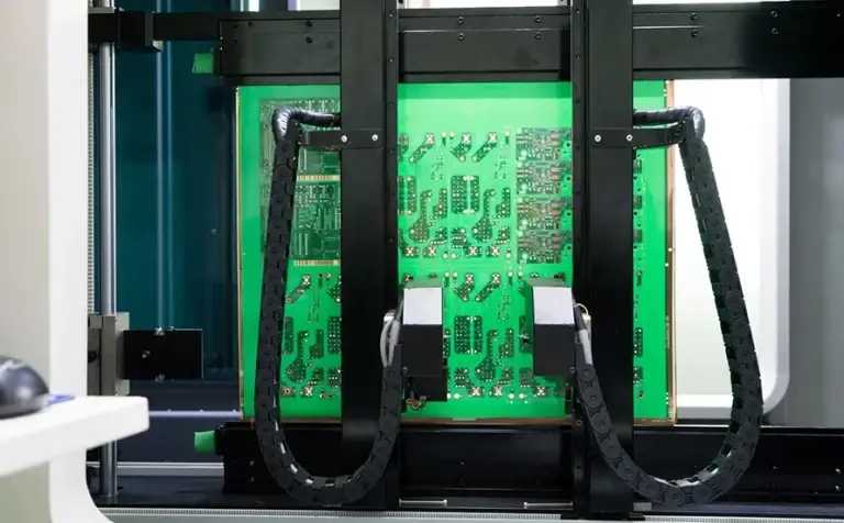
Stable Contact with the Bare PCB
Many factors can influence probe readings, including board movement, poor board support, oxidation, contamination, or an unstable probe target. Before interpreting a reading as a copper-network defect, the operator confirms alignment, support, surface condition, and repeatable access to the electrical contact point.
Dense probe targets, thin flex regions, and unsupported areas require additional attention because the probe may deflect the board or fail to land consistently. Contact planning for the test procedure must match the target geometry and the board's supported test state.
A repeat measurement is controlled only when the same net, contact location, board support state, equipment configuration, and test condition are maintained. A reading that clears after contact is re-established is treated as a contact-related indication. An indication that repeats under the same conditions is documented as a board-level failure.
Initial Continuity and Isolation Results
The first run yields either a pass or a failed relationship associated with the affected net, contact locations, measured values, test criteria, and test conditions. A failed indication undergoes contact, data, and revision checks before the same relationship is retested.
Keeping the original test results together with the repeated results allows transient access problems to be distinguished from repeatable electrical faults. The final test result therefore reflects the confirmed outcome rather than only the first machine indication.
Selecting Flying Probe or Fixture Testing
The testing method is usually determined by the specific design lifecycle rather than a single order-quantity threshold. Flying probe testing provides greater revision flexibility and eliminates the need for dedicated tooling, which can reduce initial setup costs. Fixture testing becomes more efficient after the test contact pattern has stabilized and recurring volume can recover the fixture preparation cost.
| Test method | Contact architecture | Fixture | Revision tolerance | Cycle behavior | Best production state |
|---|---|---|---|---|---|
| Flying probe | Sequential movable probes | None | High | Scales with point count and measurement type | Prototype / lower cumulative quantity / active revisions |
| Fixture test | Parallel bed-of-nails contact | Dedicated | Low | Short recurring cycle after fixture setup | Stable design / recurring production |

Flying Probe for Changing Designs
Flying probe testing is not free from the need for preparation. Like sequential probing, flying probe testing requires controlled data, reachable target test points, and repeatable contact at all programmed contact locations. The number of test points and the type of measurement conducted at each test point determine cycle time. It may not be feasible to access some test points due to physical limitations in target access, regardless of how easy the program is to update or change.
Fixture Testing for Stable Production
With test fixtures, parallel contact significantly reduces the recurring test cycle time for an established product. However, a test fixture's true value depends on declared, repeatable target points. Therefore, the test fixture design and manufactured alignment must accommodate the specific requirements of the established manufacturing panel or final target geometry. Moving, removing, or resizing test locations may require fixture modification.
The project may start with flying probe testing while revisions are active and transition to fixture testing once the project design has stabilized and long-term production requirements exist. When deciding between flying probe testing and fixture testing, the following factors can help determine which option to choose: cumulative repeat quantity, accessible point count, fixture preparation time, target cycle time, and future revision probability. The overall time saved across later production lots must outweigh the costs associated with tooling and change exposure.
Netlist Accuracy Controls Test Coverage
To establish electrical net coverage as credible, the electrical test program must represent the correct design, the selected test method must reach the mapped electrical test targets, and the test report must name the population measured.
| Coverage control | Required input | Failure mode | Reporting effect |
|---|---|---|---|
| Electrical intent | CAD netlist or agreed fabrication-derived data | Program represents wrong connectivity | Results lose design-intent traceability |
| Revision match | Board / fabrication data / test program on same revision | Correct program applied to wrong board | False pass or false fail |
| Independent comparison | CAD and fabrication-derived differences resolved | Fabrication-data error enters test program | Program rests on incorrect input |
| Contact availability | Mapped targets reachable by selected method | Mapped relationship cannot be contacted | Accessible and inaccessible nets reported separately |
| Approved exclusions | Named excluded nets and technical reason | Untested relationship omitted from result | Reported coverage exceeds executed range |
| Coverage denominator | Declared population: boards / nets / points | ‘100%’ statement lacks denominator | Board population separated from test coverage |
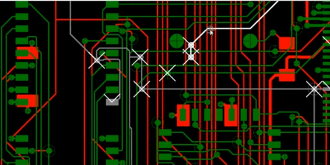
How Does a CAD Netlist Expose Fabrication-Data Differences?
The released CAD netlist represents the approved design intent and describes how the product is expected to be electrically connected. The data derived from the fabrication process show how the board was physically interpreted based on the connectivity contained in the manufacturing files. These data sets can be compared to identify connections that are missing, merged, or changed before a fabrication-data error appears in the test program.
SUGA preserves each individual data source, reconciles the differences before execution, and documents which source provides the basis for the completed test program. A manufacturer's fabrication output is not considered design intent solely because the test program can import its data.
Netlist Revision Matching
When a design changes, both the controlled test program and the physical contact map must also change to reflect it. No technically valid result can be produced when the net definitions or target coordinates belong to another revision.
IPC-D-356B is a standard for transferring bare-board electrical test data and does not replace or serve as an acceptable form of revision control by itself. SUGA matches the selected data source, executable program, physical board, and revision before running any tests.
Electrical Test Coverage Denominator
The electrical test coverage denominator is determined by the board population, net population, and physical point population. “Each board tested” means every bare PCB enters electrical testing; it does not mean every net is reachable, every point is contacted, or every possible fault mode is detectable.
Consequently, the report separates boards, executable nets, contacted points, and approved exclusions. Approved exclusions and inaccessible targets remain listed with explanations so that they do not disappear into one coverage percentage.
Engineering can assess untested relationships based on circuit function. A redesigned test pad, a different probe target, a fixture contact change, or another circuit access method can then be attributed to a specific net instead of being treated as an undefined coverage gap.
Electrical Test Settings
SUGA supports bare-board continuity tests, isolation tests, high-voltage tests, fixture-contact tests, and fine-pitch flying-probe tests. The executed report lists the threshold, applied voltage, target contact method, covered population, and exclusions used for the tested board revision.
| Electrical setting | Capability / range | Control type | Test target |
|---|---|---|---|
| Continuity threshold | ≤0.1 Ω | Supported pass threshold | Intended conductive paths |
| Maximum applied voltage | Up to 1000 V | Equipment capability | Isolation / specified HiPot |
| Isolation criterion | 25 MΩ to 2 GΩ | Selectable programmed range | Separated nets / voltage regions |
| Fixture contact pitch | 0.020 in / 0.508 mm | Contact geometry benchmark | Dedicated fixture test |
| Flying-probe contact pitch | 0.004 in / 0.102 mm | Contact geometry benchmark | Fixtureless test |
A capability limit indicates what the equipment can apply; the program setting records what was actually applied; and the pass threshold determines whether the measured result is accepted. The “Continuity Threshold ≤0.1 Ω” value remains supported, but the selected criterion for a given board is based on the approved electrical requirement for that specific board.
When a project has adopted IPC-9252B as the project requirement for an unpopulated board, SUGA retains the defined test level, test conditions, program version, and result basis with the identified board revision.
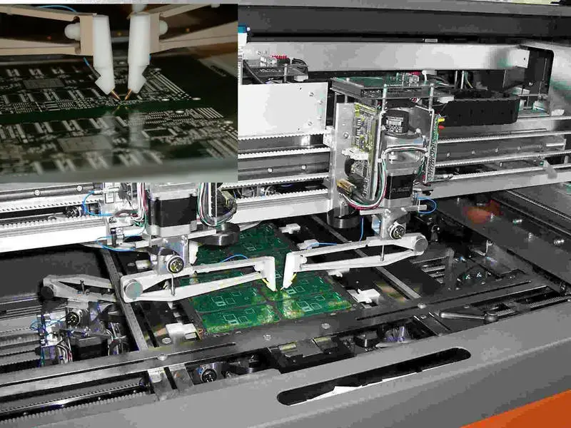
Continuity Pass Threshold
The continuity criterion establishes a clear pass/fail basis for each path measured in the test. Typically, high-current power planes and ground returns run close to the supported ≤0.1 Ω threshold, while criteria for other nets are defined by the board requirement rather than the maximum capability of the test equipment. Thus, the report must show the actual criterion used for the measurement rather than treating the supported capability as a blanket criterion for all circuits.
If the measured value exceeds the criterion, the measured value is retained, and the affected net and locations are recorded so that the technician can confirm the result. This differentiates between a measurable high-resistance path and a complete open circuit; therefore, both failures are not reported under the same failure heading.
Isolation Resistance and Applied Voltage
Isolation resistance defines the required electrical separation between two networks; the applied voltage defines the condition under which that separation is measured. Both values are identified in the board requirement and incorporated into the measurement results.
When performing isolation and HiPot tests, the equipment may operate up to 1000 V; however, continuity tests do not use the maximum voltage level. If a continuity test inadvertently uses a HiPot-level voltage, it could stress a low-voltage-rated structure on the PCB. For this reason, the voltage used for continuity testing is programmed based on the net category rather than the maximum equipment voltage. The actual voltage and isolation criterion are recorded so that the pass decision remains linked to the specified test conditions.
Electrical Contact Access
When discussing electrical contact access, it is important to differentiate between the physical pitch of the contact locations on the PCB and their electrical acceptance. Fixed test fixtures have a defined contact layout, while flying probes can test programmed target locations without dedicated fixed tooling.
The contact-pitch geometries of 0.020 in for fixtures and 0.004 in for flying probes indicate what the equipment may be able to access; however, they do not guarantee that all targets at the specified pitch can be tested on every PCB. Other factors that affect access to PCB pad locations include pad size, adjacent copper, solder mask clearance, probe approach angle, pad surface finish, board support during testing, and local board warpage. Therefore, SUGA validates the actual contact map against the physical board before approving access based solely on contact pitch.
Network-Specific Measurements
Controlled-impedance nets can have their specified impedance confirmed at named locations using TDR. The four-wire Kelvin measurement method can be used to separate lead and contact resistance from the current-path resistance. Specified isolation regions of a PCB can be tested using a HiPot tester with a defined voltage, duration, and acceptance criterion. Although these test methods provide network-specific measurements, they do not replace the need for open-and-short testing.
The TDR method cannot indicate the full channel’s insertion loss, crosstalk, or eye-pattern performance; the Kelvin test method does not indicate the temperature rise that will occur while current is carried through a circuit; and the HiPot method applies only to the regions and conditions defined in the bare-board test requirement.
PCB Electrical Testing Applications
Continuity and isolation remain the base checks across applications; however, the critical networks and failure modes that differentiate each application depend on the PCB design before components are assembled.
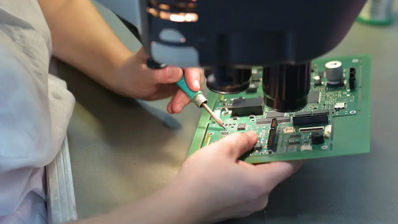
Aerospace and Defense Control Boards
Aerospace and defense PCBs traditionally include combinations of I/O connectors, power and ground connections, and long via-chain routes on high-value, low-volume assemblies typically built to IPC-6012 Class 3 requirements. Because of the critical nature of the application, the test program should always correspond to the specific PCB revision and lot, since an incorrect revision pairing can produce an invalid measurement, and retesting can add cost to the project schedule.
A static continuity test through a via chain confirms the present electrical connection at room temperature. It does not detect a hairline crack in the via wall that opens only under thermal cycling. Therefore, when plating and environmental qualification requirements apply, the electrical test results should be interpreted alongside the relevant plating and environmental qualification data.

Medical and Sensor Electronics
Medical and sensor PCBs often include low-level signals close to sensitive power and isolation regions. IEC 60601 patient-safety requirements apply downstream of the bare board. Bare-board testing before assembly can detect opens, shorts, and abnormal leakage between named nets; however, a passing bare-board isolation test is not equivalent to a patient-leakage current test performed on the assembled device because the tests are defined by different requirements and performed at different stages.
Residue and surface contamination can reduce the measured isolation resistance. Therefore, the condition of the board and its contact surfaces must be controlled during confirmation testing to avoid misinterpreting an electrically acceptable board as a marginal failure.

Automotive and Industrial Control Boards
Automotive and industrial control boards typically combine power domains, grounds, control I/O, drive outputs, and relay interfaces into one board, with relevant components potentially subject to AEC-Q200 qualification and manufacturing processes managed under IATF 16949 requirements. For example, a bus bar or relay drive return, both of which are very-low-resistance connections, typically requires a four-wire Kelvin measurement to avoid bias from the contact resistance of a two-wire connection; otherwise, the contact resistance may dominate the measurement before the copper conductor itself becomes suspect. Another example of a net with parallel branches is a redundant ground strap or split power planes. Since there are separate routes through which measurements can be made, each branch must have its own access points; otherwise, the complete net may pass while one branch remains open, leaving the fault hidden.
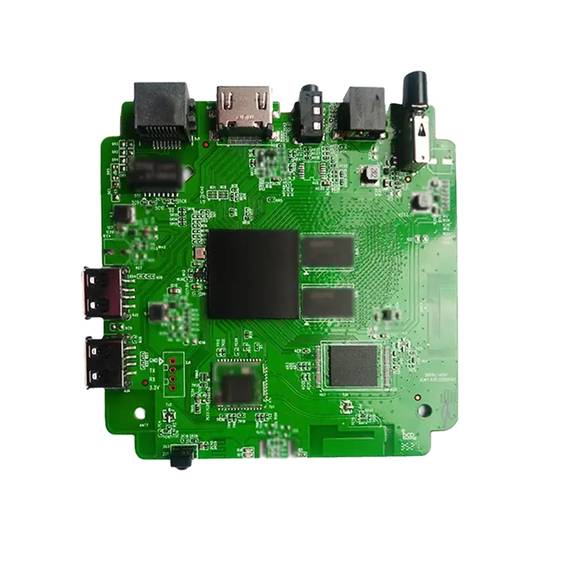
Telecommunications and Computing Boards
Telecommunications and computing boards typically have dense connector routing placed adjacent to closely spaced controlled-impedance networks. Most telecommunications and computing devices use either 50 Ω single-ended or 100 Ω differential-pair routing on backplanes and SerDes networks. Since revisions may use different routing layouts, it is important to identify where each connection route can be accessed and to update the revision-specific contact map whenever routing changes are made. Otherwise, test coverage for the new revision may be degraded without being evident. Continuity and isolation testing will identify mapped open and short circuits, while TDR will confirm the impedance of specified traces against a 50 Ω or 100 Ω target; however, neither result indicates channel insertion loss, crosstalk, or eye-diagram performance.

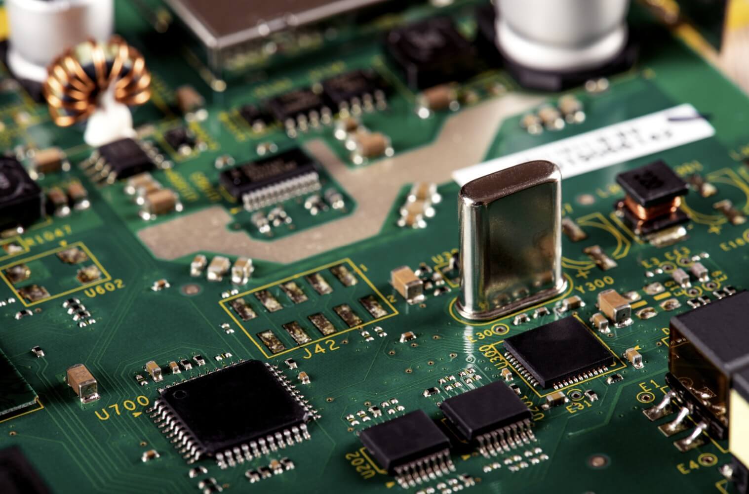
Energy and Power Electronics
Energy and power PCBs are required to have low-resistance current paths. These paths often carry tens of amps through bus bars or heavy copper pours. Energy and power PCBs require clearly defined separation between voltage regions. In some cases, these regions can exceed 400 V, depending on the application, including EV and grid-tied designs.
Kelvin measurement is an appropriate method for verifying specified very-low-resistance paths. Two-wire contact resistance can affect the measured value and mask the actual conductor resistance. To test insulation integrity and isolation, a HiPot test must be performed with a specified voltage, duration, and acceptance criterion for each isolation region; a single blanket voltage across the board is not sufficient. Bare-board testing can confirm the copper network under the test conditions, but it cannot demonstrate copper-path performance under operating temperature-rise and current-carrying-load conditions.
HDI Connected Devices
HDI and connected-device PCBs often contain a high density of nets concentrated around small targets and plated microvia structures. These boards are typically designed according to IPC-2226 guidelines and contain stacked or staggered microvias between PCB layers.
SUGA supports 0.004 in / 0.102 mm flying-probe contact as an equipment benchmark for microvia targets. However, pad geometry, probe configuration, board support, and surface conditions can affect whether a particular microvia target is reachable at a given net density. A static continuity test performed at room temperature can demonstrate that the microvia stack is electrically connected. However, it cannot confirm whether the microvia is partially plated or thermally compromised and may open only after reflow or thermal cycling in service.
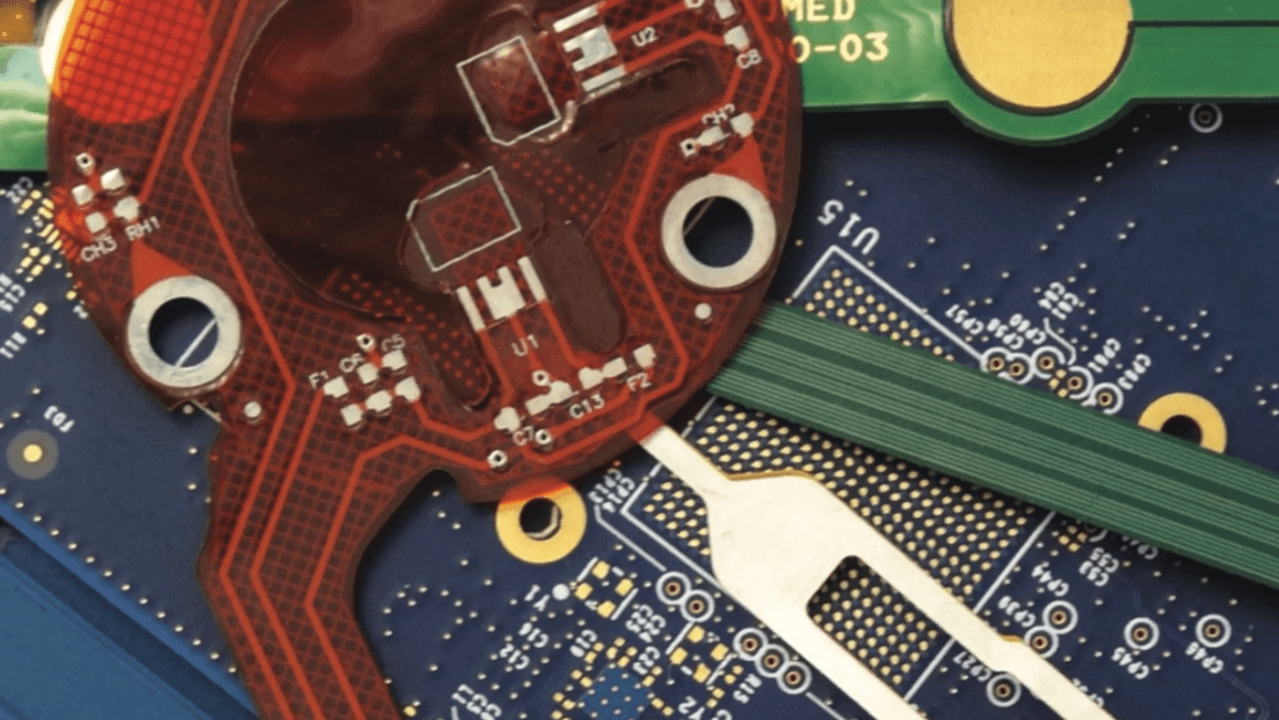
Flexible and Rigid-Flex Boards
When flexible and rigid-flex PCBs are tested, it is necessary to control the support across the rigid, transition, and flexible regions of the board. The test report should specify how the board was held during testing. The flex zone of a PCB can behave electrically differently depending on how it is supported during the test; bending, probe force, or another external load can create an intermittent connection that is recorded as a pass while flexed but disappears or appears as an open once the board is flattened or re-flexed.
A passing static E-test indicates only that the PCB was electrically connected in the recorded test state. It does not demonstrate dynamic flex life after repeated use in service, so separate qualification testing is required for PCB designs that flex repeatedly during operation.
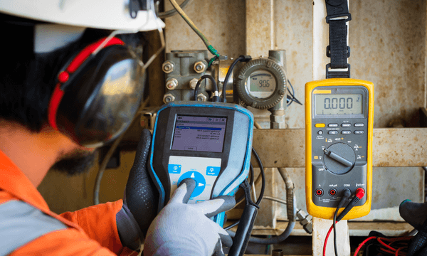
Test and Measurement Equipment
PCBs used in test and measurement equipment require correct mapping of analog inputs, digital controls, reference signals, guards, shields, and isolated power regions. A single misrouted channel can shift a downstream calibration value without producing an obvious fault. Failed-net documentation should include the channel identity to differentiate a localized copper-network failure from subsequent calibration error, noise, or component-level problems encountered during board bring-up.
Continuity and isolation tests on bare printed circuit boards can confirm the correct copper connection in each channel before component installation; however, passing these tests does not guarantee assembled performance, acceptable noise levels, or calibration traceability.
Electrical Test Results and Failure Traceability
A failed-net status provides useful information only when it is associated with the correct board or panel and the condition under which the failure occurred is identified. Failed-net documentation allows recurring electrical signatures for a given lot to be compared with manufacturing evidence to determine whether an ongoing electrical failure is associated with a manufacturing defect.
| Result record | Required field | Engineering action |
|---|---|---|
| Board / lot identity | Panel, board, and production-lot IDs | Match board or panel to recorded result |
| Program / revision | Approved board revision and test-program version | Confirm program-to-board match |
| Failed net | Net ID and affected locations | Repeat the same net or path |
| Measured value | Reading, criterion, and initial status | Confirm repeatability under the same condition |
| Contact / data check | Contact state, surface condition, and test-data findings | Eliminate contact, surface, or data causes |
| Retest | Repeated condition and final outcome | Compare initial and repeated results |
| Manufacturing feedback | Confirmed failure type and relevant process area | Review production evidence before assigning cause |
Failed-Net Identification
A generic board-fail label provides no direction for what an engineer must repeat. A failed-net record retains information such as the net identifier, affected location(s), measured value, criterion, applied condition, and initial status so that the same electrical relationship can be verified.
The identity of the circuit board and its revision determines whether the evidence can appropriately support a disposition decision. If a valid measurement is linked to an incorrect board, panel, lot, or program version, that measurement cannot be used as the final result for that board.
Retest and Final Board Result
Retesting a net begins after the contact condition, surface condition, data source, and program identifier have been checked. Repeating the same electrical relationship under the recorded condition separates a temporary access or program issue from a repeatable board failure while preserving both the original status and the retest result.
Recurring Failure Patterns
Failed-net signatures are grouped according to the type of failure, network location, lot, and revision. Multiple signatures associated with a particular electrical network location may direct engineering to investigate drilling, plating, etching, imaging, or handling evidence when the electrical location supports that investigation.
Comparing the frequency of a recurring failure pattern before and after corrective action can provide evidence of whether the manufacturing change removed the pattern without determining root cause solely from an electrical measurement.
Our PCBA Production Lines
















PCB Electrical Testing FAQ
Cost is determined by program preparation, fixture preparation when used, the number of accessible points, the quantity of panels tested, design revisions, the type of measurement, recurring cycle time, and retest exposure. Testing with a flying probe eliminates the investment required for a dedicated fixture, while using a fixture can reduce recurring test time for a stable, repeatable design.
The amount of time required for PCB electrical testing depends on program preparation, the number of accessible points, the test method used, the type of measurement performed, the number of panels tested, contact condition, and whether retesting is required. A changing prototype tested by flying probe has a different setup and cycle-time profile from an established, repeatable design tested with a fixture.
Yes, but the level of assurance provided differs according to the data basis. If a CAD-generated netlist cannot be provided, fabrication-derived connectivity can be used to define an open-and-short test program; however, this data cannot independently verify that the manufacturing data match the original design intent.
A buyer without an exportable netlist should request the report section that identifies the data source, tested networks, accessible locations, and approved exclusions.
No. A multimeter cannot perform automated PCB testing as defined by a netlist-driven test program. A multimeter may be used to check selected points during bench diagnosis; however, it cannot test mapped locations throughout the bare-board layout or provide the same board-linked record of program revision, test settings, coverage, and exclusions.
Yes. SUGA performs electrical testing on every bare PCB it manufactures. “Every board tested” defines the population of PCBs entering the electrical test process; the report also identifies the networks or points included in the program, the contact method, the actual settings used during testing, and any inaccessible or approved exclusions.