Upload BOM & Gerber
-
Mobile: +86 13312967631
-
Email: sales@sugaintl.com

PCB In-Circuit Testing Services
Fixture-Based ICT Testing from a PCB Assembly Manufacturer in China
Align probe access, test-point geometry, electrical measurements, and coverage extensions before volume production. SUGA integrates fixture contact, programmed measurement, component-level diagnosis, repair, and retest for repeat production.
100–10,000+ Nets Supported
Up to 5,760 Test Nodes
20 × 128-Pin ICT Cores
What In-Circuit Testing Detects
In-Circuit Testing provides information on the electrical state of components and nodes on an assembled PCB, together with component- and node-level measurements. Powered operational PCB functionality is covered by functional testing, AXI examines internal solder-joint structures, boundary scan tests supported interconnects and components, VTEP or touch-probe testing extends coverage to component terminals with limited direct access, and environmental testing addresses vibration, temperature, or load-related behavior.
| Test object | Measurement basis | Failure indication |
|---|---|---|
| Passive values | R, C, and L measurements against programmed limits | Wrong value or out-of-tolerance component |
| Polarity | Directional electrical signature | Reversed diode, polarized capacitor, or selected IC orientation |
| Open path | Continuity between accessible nodes | Lifted pin, missing connection, or broken conductive path |
| Short path | Low-resistance isolation check | Solder bridge or unintended net connection |
| Part presence | Expected signature compared with measured response | Missing part or selected wrong-part substitution |
| Solder electrical effect | Node continuity and component response | Lifted lead, conductive bridge, or tombstoned open |

Component Measurements
ICT programs specify methods and performance parameters for measuring resistance, capacitance, inductance, voltage, and other responses at accessible component connections and nodes.
ICT provides tolerance limits based on the performance of individual components, circuit topology, and reference values from known-good boards. In certain cases, the electrical characteristics of an individual R, C, L, diode, polarized capacitor, or selected Integrated Circuit (IC) response may be determined directly unless the test result is influenced by parallel connections.
Individual component test responses may be masked by parallel paths and pulled within acceptable test limits. Guarding, isolation, or cluster testing, when topology allows, separates the contribution of the individual component from connected components; otherwise, the ambiguous network is subjected to powered testing or another electrical method.
Connectivity Faults
Continuity and low-resistance tests are helpful in identifying breaks or unintended connections within a circuit; however, a failing result at a node does not automatically indicate a defect within the board. A repeated failure at the same node might point toward problems with the conductive path; however, a changing result may lead to a thorough investigation of probe contact, contamination, alignment, seating, or local board support.
A high-resistance or intermittent failure may occur only when the circuit is subjected to vibration, temperature, electrical load, or mechanical movement; therefore, the troubleshooting process must include testing under the corresponding powered or environmental conditions.
Electrically Visible Assembly Faults
A missing or incorrect part will cause the electrical signature on the PCBA to deviate from the programmed electrical signatures at its nodes. When access to a component and the PCB circuit topology allow the responses of absent, incorrect, or reversed parts to be separated, ICT can identify them.
Three main assembly faults due to thermal and mechanical imbalance can cause electrical open or short signatures similar to those of missing, incorrect, or reversed components. The causes behind these three signatures are uneven paste volume or an oxidized pad pulling a two-terminal component into a tombstone position before the reflow process is complete, thermal-cycle stress on a marginally wetted joint lifting the lead over time, and bridging in dense fine-pitch fields where paste-volume control is more difficult. Once the failure opens an accessible node or shorts two terminals, ICT will identify the electrical open or short. A joint that appears structurally compromised under AXI or AOI but has not changed the electrical path remains an inspection finding rather than an ICT failure.
How PCB In-Circuit Testing Works
A fixture-based ICT cycle follows five actions:
- Load and align the PCBA. Tooling features position the board or panel against the fixture probe field.
- Establish probe contact. Controlled pressure brings spring probes onto the selected pads, vias, or leads.
- Apply stimuli and measure responses. The program captures resistance, capacitance, voltage, continuity, or a programmed powered response.
- Compare results with limits. Software assigns a pass or a component- or node-level failure.
- Record the result. The outcome is stored with the board serial or lot identifier, fixture revision, and program revision.
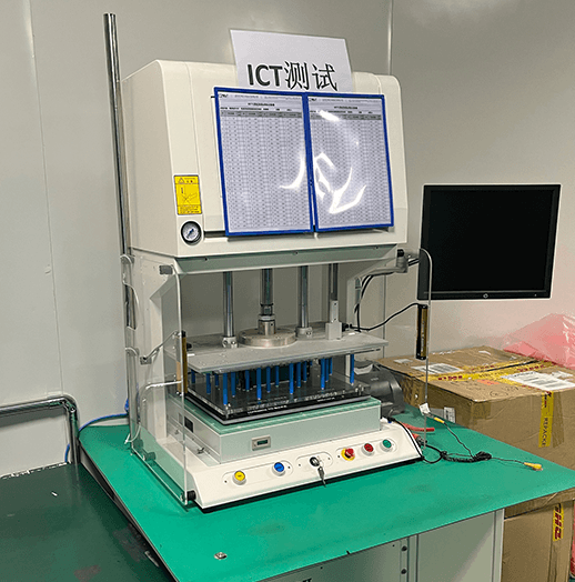
How Does the Fixture Contact the PCB?
The tooling features ensure that the board is positioned correctly relative to the probe plate; board supports keep the entire assembly in the required plane. Too little probe travel creates intermittent contact due to insufficient contact force; poor alignment places a probe tip on the edge of the solder mask; excessive or uneven force can bend the board around dense probe areas, large connectors, or unsupported board regions.
The fixture may contact the PCB on one or both sides, depending on the arrangement of the components, distribution of targets, board support system, and handling direction. Stage, clamshell, wired, wireless, pneumatic, and vacuum configurations provide different loading, signal-routing, and actuation methods.
How Are Electrical Measurements Applied?
Once stable contact is established, the program routes the measurement resources to the appropriate test nodes. Passive-value checks use minimal stimulus levels, while continuity and voltage checks use the measurement path defined in the program; powered extensions require current limiting, sequencing, stabilization, and discharge under certain conditions. Acceptance limits are defined by the allowable tolerances of the components being tested, the characteristics of the overall circuit being tested, correlation data, and the intended diagnostic resolution.
Which Tester Capacity Matches the Board?
Net count refers to the connectivity of the board. Test nodes are points that can be accessed, switched, or tested. Pins provide the configured connection capacity; ICT cores refer to the amount of parallel execution resources available. All these categories are assigned separately when determining tester resources that are appropriate for testing a specific board or panel.
| Resource dimension | Available capacity | Assignment basis |
|---|---|---|
| Project net complexity | Fewer than 100 to more than 10,000 nets | Accessible nodes, measurement types, and board construction |
| Inline node capacity | Up to 5,760 test nodes | Tester platform and pin-card configuration |
| Parallel ICT resources | Up to 20 × 128-pin cores; up to 2,560 combined pins | DUT count, core allocation, and separate pin, net, and node limits |
Fixture Configuration
The configuration of the test fixture can vary greatly depending on the number of DUTs to be tested simultaneously. Single-DUT fixtures will have only one DUT in contact with the fixture for the complete test cycle. In contrast, multi-DUT fixtures may have multiple DUTs in contact with the same fixture for testing; however, all measurement and timing resources must be available and switchable, and a separate DUT identifier must be assigned accordingly. Parallel contact improves takt only when the tester can supply the complete switching and measurement resource demand. Component height and probe density also determine probe-plate openings, mechanical clearance, local board support, and fixture service access.
The fixture must be configured based on the final probe map instead of a generic board type. When the tooling, mechanics, and probe access are the same, a single fixture base can accommodate multiple variants. Inserts, probe plates, or individual programs can handle the differences between variants, while each variant will still keep its own coverage, limits, DNP logic, and board or panel-position record.
Developing the ICT Test
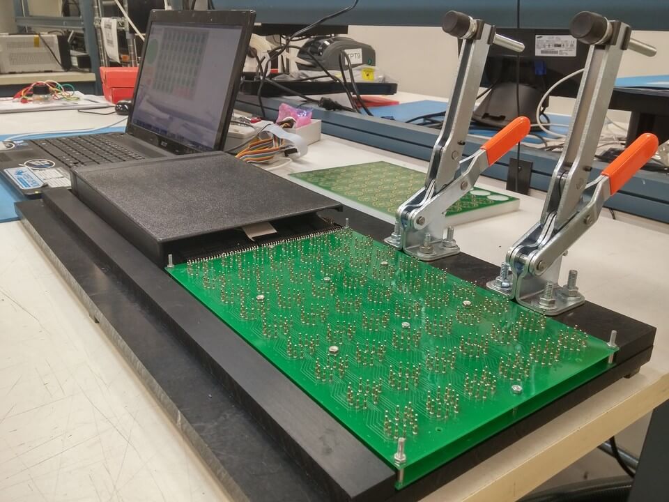
In developing the ICT test program, typical inputs may include a netlist, BOM, schematic or CAD data, component-library information, known-good boards, and any debug measurements taken on those boards. The information associated with these inputs supports accurate connectivity data, automatic test generation, shorts coverage, diagnostic accuracy, and up-to-date revision tracking. The use of known-good (KG) samples assists in establishing correlation; however, this should not be viewed as a replacement for complete connectivity data.
Prior to repeat production, SUGA will verify the suitability of the measurement methods, limits, diagnostic output, coverage statement, and the match between the fixture and program. The production record will document the revisions of the fixture and program, measurement details, diagnostic output, the coverage statement, and the format of the board-level results.
Powered ICT Extensions
Powered ICT extensions can test LEDs, capture ADC and DAC responses, program EEPROM and Flash memory, perform I2C and SPI routines, and conduct selected controlled-power tests on specified portions of the device. In-system programming may remain in the same cell when the PCB architecture supports it. It should support write verification or read-back, current limits, power sequencing, stabilization, and discharge where required. The programming results and firmware version are stored as part of the board record; programming failures will be reported separately from component or connection failures. FCT will verify that loaded interfaces, actuators, firmware interaction, and complete product behavior operate as intended.
How Do PCB Revisions Affect ICT?
A revision to the PCB will directly affect the probe map, fixture plate, fixture support, wiring, component models, programmed limits, and verification work. A change in value might require only a program change. A moved target will typically require an insert or probe-plate change; a new outline or mechanical arrangement typically requires modification or replacement of the existing fixture.
ICT or Flying Probe?
Fixture-based ICT tests use a fixed spring-probe field and a board-specific fixture to contact multiple planned points in parallel; therefore, fixture-based ICT is an excellent choice for stable released designs, ongoing production, and takt-sensitive purposes. PCB changes will affect the probe map, fixture mechanics, wiring, and ICT program.
Flying probe uses independently controlled moving probes and does not require a bed-of-nails fixture. These systems may use 8 or more independent probes, based on the selected configuration. The serial travel of each probe produces a longer cycle but provides more flexibility in absorbing layout revisions through software changes than fixture-based ICT; therefore, flying probe is generally most practical for prototypes, engineering samples, and revision-heavy New Product Introduction (NPI).
Selection depends on design stability, available targets, repeat production volume, and production takt. If a board is very compact, it may stay on flying probe during design revisions, and once the test-point field, outline, repeat forecast, and cycle time have stabilized, it can transition to fixture-based ICT. Flying probe will continue to support NPI and subsequent revisions, while the fixed fixture controls the released production version.
PCB Test Point Design
An ICT-ready PCB provides a stable datum, reachable targets, component clearance, board support, and suitable return paths. The following values are engineering starting points for the selected probe and fixture architecture.
| DFT control | Engineering target | Fixture condition |
|---|---|---|
| Tooling datum | Stable PCB or panel tooling holes | Diameter, tolerance, and panel datums |
| Probe side | One-sided target field where practical | Dual-side access when placement or coverage requires it |
| Primary target | 30 mil diameter or larger | Layout area and electrical design permit |
| Guided target | 24 mil minimum | Guided probes and controlled registration tolerance |
| Mask opening | Entire probe landing area exposed | Fabrication registration and target tolerance |
| Component clearance | Space for probe barrel, receptacle, and plate opening | Probe family and neighboring component geometry |
| Edge clearance | Target center at least 0.125 in from board edge | Fixture wall, support, and panel-rail geometry |
| 100 mil probe family | 85 mil center-to-center | Barrel and receptacle dimensions |
| 75 mil probe family | 70 mil center-to-center | Neighboring component and plate clearance |
| 50 mil probe family | 50 mil center-to-center | Tighter machining and alignment |
| 39 mil probe family | 39 mil center-to-center | Highest listed precision and maintenance demand |
| Board support | Support under dense fields, large connectors, and sensitive areas | Board thickness, underside parts, and probe distribution |
| Fixture force | Maximum 96 oz/in² distributed load | Recalculate for support spacing, probe count, and component height |
| Ground nodes | Approximately 10% of connected nodes | Measurement topology and return-path demand |
| Contact priority | Test pad → exposed via → through-hole lead | Most stable serviceable contact surface |
| Probe via | Exposed surface with compatible finish | Covered or unreliable surfaces excluded |
Fixture Alignment
Fixture alignment for tooling holes also needs to correspond to the production panel, datum structure, and loading direction. Tooling rails of the breakaway type can provide tooling-feature locations as long as they remain rigid during loading and do not interfere with support or depaneling. Changes to a rail, a mismatched datum structure, or reversal of the loading direction will move the entire probe field, causing repeated false calls across the same area of the board.
One-sided access simplifies the fixture design; however, higher-density placement or coverage requirements may necessitate dual-side probing. In addition to satisfying all measurement requirements, the access plan should not create unsupported areas or conflict with the production handling direction.
Target Geometry
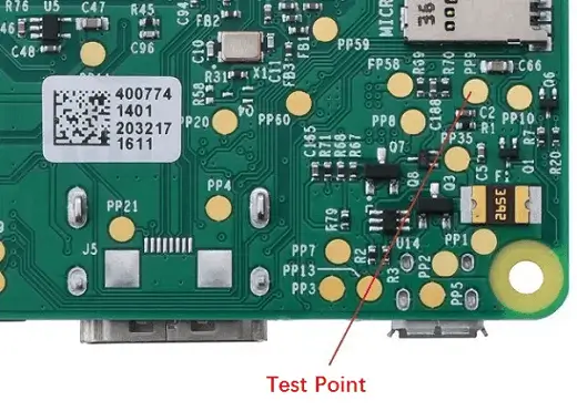
The finished solder-mask opening must expose the entire landing area, and the component body and fixture openings must provide sufficient surrounding clearance. The target diameter and the spacing of the probe family are two separate control mechanisms. The 30 mil and 24 mil measurements define copper landing areas; the 100, 75, 50, and 39 mil families define the probe and receptacle geometries. The family mil designation indicates the standard mounting-center convention but does not define the barrel diameter; for instance, the 100 mil family has an 85 mil minimum center-to-center spacing. Each family must still be verified against the specific probe, receptacle, and plate geometry selected for the board. Mask registration may also decrease the usable area available within the solder-mask opening, even when the copper target meets the nominal diameter.
Smaller targets with tighter spacing will increase manufacturing, alignment, tip-selection, and maintenance demands. Adequate spacing between centerlines does not necessarily provide sufficient clearance for a probe barrel, receptacle, plate opening, and the body of neighboring components.
Board Support
Adequate board support underneath areas of dense probing, large connectors, thin boards, and mechanically sensitive areas is required. The distributed-force limit of 96 oz/in² does not negate the need for an evaluation of the mechanical performance of the board because probe count, spring force, support distance, board thickness, and component height affect local stress. Excessive local deflection will reduce the available probe travel and create random opens or contact-verification failures, even if a sound electrical path is established.
Ground allocation supports measurement stability. Ground allocation typically includes approximately 10% of the total number of connected nodes; however, sensitive analog measurements or other return-path topologies may require a different distribution.
Target Selection
Dedicated test pads will generally provide the most repeatable landing surfaces because their designs and finishes are created specifically for probing. When exposed vias are the only viable option, they can be used only if their opening, finish, registration, and long-term contact stability are consistent. Through-hole leads are selected when they provide the most serviceable exposed point without affecting the component body or solder joint. Even though a point may be reachable on the same network, that does not necessarily mean it will be the best production target: contact-tip wear, contamination, oxidation, angled contact, and surface damage can all affect false-call rates throughout the life of the fixture.
ICT vs Functional Test
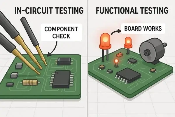
ICT tests components and their electrical connections while the PCBA is unpowered or selectively stimulated and checks values, polarity, opens, shorts, and node responses. In the case of an open or short, ICT will localize the failure to a component or node. Functional testing powers the board under controlled conditions to check voltage rails, I/O, protocols, firmware interaction, and operating outputs. Functional test results identify the operating behavior of the board rather than provide component-level diagnosis.
A typical testing sequence is AOI/AXI if applicable → ICT → diagnosis, repair, and retest → FCT → complete system validation. The exact sequence of testing will depend on product risk, inspection configuration, programming requirements, and the powered-test configuration.
ICT identifies structural manufacturing faults before functional-diagnostic time is spent looking for them. FCT then confirms operating behavior that cannot be verified by ICT when the PCBA is unpowered or selectively stimulated. Complex PCBAs can benefit from both ICT and FCT because one powered symptom can have a component, firmware, connection, or system cause.
ICT Cost and Cycle Time
| Cost driver | Takt and cost effect |
|---|---|
| Fixture tooling | One-time board-specific cost for probe plate, support, wiring, and actuation |
| Test development | Generation, models, limits, debug, diagnostics, and qualification effort |
| Sequence content | Measurement count, settling, programming, powered checks, and discharge time |
| Mechanical handling | Load, align, actuate, and unload time per cycle |
| Parallel DUTs | Fixture and handling time shared across supported circuits |
| Retest / false calls | Contact verification and diagnosis added to effective takt |
| Fixture service | Recurring probe, contact, wiring, alignment, and support maintenance |
| Repeat volume | Setup investment amortized across more boards |
| Early localization | Reduced downstream functional debug and repair effort |
ICT Setup Investment
When fixture implementation and testing are initiated before the board outline and probe field are fully stabilized, the likelihood that modifications to inserts, plates, or fixtures will be required increases. There is no universally accepted production volume that determines the economic crossover point for ICT; rather, it varies according to fixture cost, required repeat cycle time, design stability, diagnostic information, and expected production life.
Program reusability is feasible only when mechanics, probe access, component options, limits, and variant logic are equivalent. For example, having a shared product name or BOM does not mean that two boards can share a common production program.
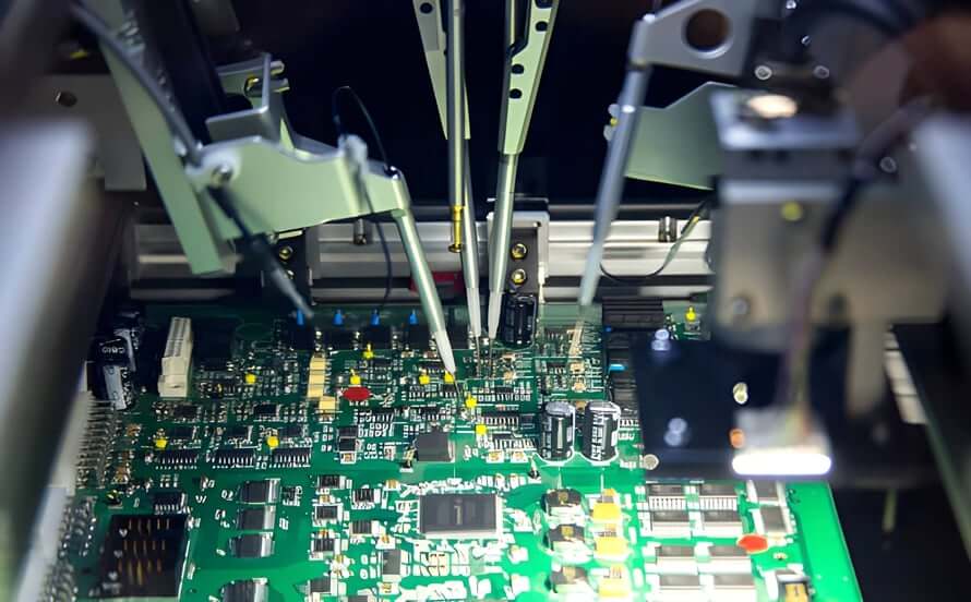
Production Cycle Time
The production cycle time for PCB ICT can range from seconds to one or two minutes.
The effective takt time combines electrical measurement, loading and clamping, fixture actuation, contact verification, unloading, failure handling, retesting of DUTs, and the number of DUTs tested in parallel. It is not defined solely by the nominal time required to complete the electrical test.
SUGA achieved a 10% increase in production throughput on an ADAS PCBA program by optimizing the complete ICT cycle. The team reviewed how measurements were executed, how fixtures were actuated, how boards were handled, how contact verification was completed, how test resources were allocated, and how failures or retests were handled. SUGA eliminated unnecessary delays around the electrical test while still meeting the requirements for all component, continuity, and short-circuit checks. The increased throughput was achieved through improvements across the entire production cycle, not by reducing test coverage.
Fixture Lifecycle Cost
Repeated failures at specific nodes on a fixture, excessive variation in probe readings, or contact inconsistencies can indicate probe wear, contamination, receptacle degradation, wiring changes, or alignment drift.
PCB revisions often add cost when they require a program change, probe-map update, fixture modification, or fixture revalidation. Maintenance trends and revision-history tracking provide insight into whether the issue belongs to the board, fixture, or program before a replacement decision is made.
In-Circuit Test Applications
For repeated PCBAs that must be tested before powered testing, ICT provides a method for isolating accessible component and connection faults.
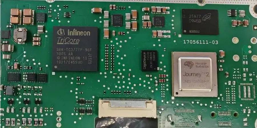
Automotive and ADAS Control Boards
ADAS camera, sensor, body-control, and interface PCBAs use ICT to validate resistor and capacitor networks, protection-device polarity, connector paths, opens, and shorts before CAN, LIN, sensor-response, load, or environmental testing. A reversed protection device on a CAN or LIN line can have significant implications; it may pass a simple continuity test but fail to operate correctly when subjected to transient conditions. As such, establishing polarity carries additional safety implications beyond first-pass yield.
In multi-DUT production, all circuits in a panel also need to be uniquely identified by either a DUT identifier or panel position so that a bad board is not obscured within the overall panel result. Local support is also required in dense connector or sensor-interface areas because uneven fixture pressure can cause contact failures that resemble opens.
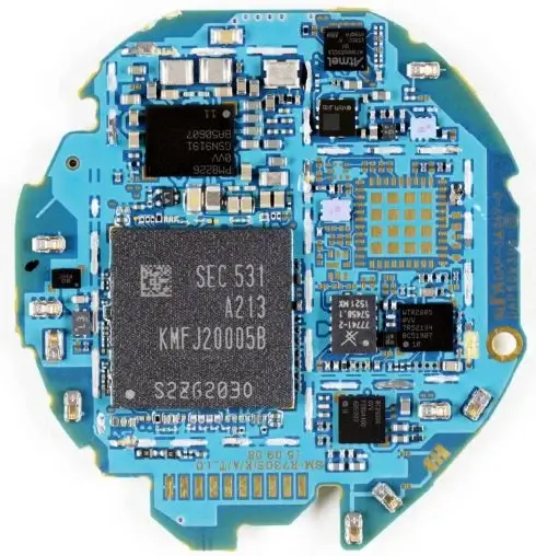
Consumer Mobile and Wearable Electronics
Compact phone, wearable, tablet, and smart-device PCBAs restrict direct probe access and leave very little mechanical room for probe barrels and board support. The polarity of battery-protection FETs continues to be an issue with these PCBAs because a reversed protection component may pass a cold continuity test yet fail to trip under an actual overcurrent condition.
ICT can identify accessible component faults, continuity issues, polarity errors, and assembly defects. Boundary scan or VTEP can extend coverage where direct probe access is limited; however, charging circuits, wireless communication systems, USB connections, battery-management systems, and user interfaces are still tested using powered methods. In addition, very thin boards and RF or high-speed designs are at risk from the indiscriminate addition of test pads; therefore, revision-heavy boards often remain on flying probe until the accessible target field and repeat-testing forecast justify a fixed fixture.

Medical Electronics
The most common medical applications of ICT include monitoring devices, control systems, imaging devices, and general-purpose instrument PCBAs. ICT checks accessible component values, polarity, opens, shorts, and connection paths before powered leakage, isolation, calibration, and functional verification. These devices must meet IEC 60601 patient-safety requirements for electrical isolation and leakage characteristics. An ICT measurement of an accessible component value is not sufficient by itself to demonstrate compliance with these requirements; a separate powered leakage-current measurement must demonstrate that the isolation and leakage characteristics meet the applicable limits.
Board and lot identifiers are used to track the history of a failed board through its repair and retest processes until it passes powered verification or calibration. While ICT is used to identify and close manufacturing defects, sensor accuracy, calibration, electrical isolation, leakage current, and complete functional performance remain in their respective test records.

Aerospace and Defense Electronics
Navigation, control, and communication assemblies for aerospace and defense applications often undergo component- and node-level localization before expensive powered, environmental, or system testing. Low-volume, high-complexity PCBAs may remain on flying probe until the repeat forecast and revision stability justify moving them to a fixed fixture.
When a substitute part has been accepted under an obsolescence waiver, it still requires its own verified component model and limit set. Reusing the original part’s program entry for a legacy-fit substitution can degrade ICT diagnostic accuracy. In long-life programs, PCB revisions, component substitutions, fixture condition, and program revisions need to remain aligned so that replacing an obsolete part does not introduce an incorrect model, limit, or probe map.

Industrial Control Systems
In industrial control systems, PLC, drive, I/O, relay, and power-interface PCB assemblies use ICT to isolate wrong component signatures, polarity errors, connector opens, relay-drive faults, and unintended shorts before rails, loads, fieldbus communication, I/O, and actuator responses are tested. Relay-drive verification during ICT checks coil continuity and drive-transistor polarity; it does not test contact life. Although a coil may measure correctly, the relay contacts may still weld shut when subjected to its full rated inrush, which can be detected only through a loaded functional test.
In some cases, shared baseboards may contain multiple DNP, voltage, or I/O variants. Each variant therefore requires a separate set of limits, distinct DNP logic, and a unique result identifier to prevent false calls caused by variant confusion. Static tests of relay coils or driver paths should not replace a loaded output test.
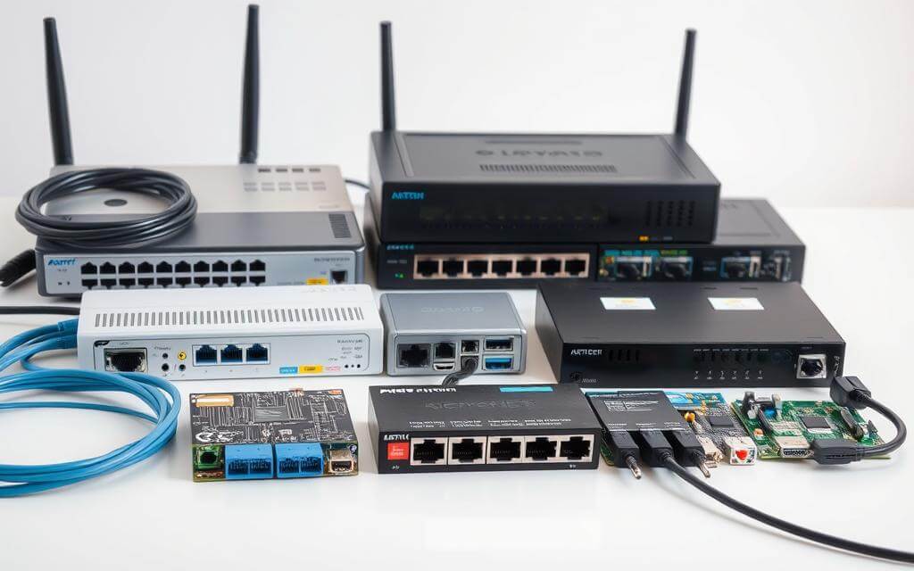
Communications and Network Hardware
Switch, router, communication-control, and interface PCBAs use ICT for power-distribution components, control networks, connector continuity, and accessible assembly faults. Critical differential and RF structures should not receive unnecessary test pads or stubs because the added geometry can disturb the signal path.
For example, removing a test pad from a differential pair to protect impedance control shifts that node’s fault coverage to boundary scan. This should be an explicit decision made during layout review rather than discovered after a coverage report identifies the gap. Boundary scan or AXI can provide selected coverage within dense-package gaps, while traffic, protocol, eye-diagram, RF, and signal-integrity performance remains at the corresponding powered or high-speed test station.
ICT Coverage Limits
ICT coverage decreases when a node cannot be accessed, a dense package hides the physical joint, an internal network lacks an observation point, or probing would interfere with a high-frequency structure. A useful coverage report separates directly probed nodes, component measurements, open and short groups, vectorless pins, scan-supported networks, and exclusions associated with the board revision.
Direct-probe, vectorless, boundary-scan, AOI, and AXI results should not be compiled into one undefined percentage. The numerator, denominator, included methods, and revision must be stated.
Access Gaps
Miniaturization restricts the space available for targets, probe barrels, fixture openings, and support. The absence of a test point creates a physical-access gap, whereas incomplete connectivity data or component models create program gaps. DFT changes are preferred while the layout remains editable.
Layer count alone does not determine coverage. An internal network must reach an accessible node or a scan-enabled device. High-frequency structures also require care because pads, stubs, wiring, and fixture contacts may change the circuit being evaluated.
Limited-Access Coverage Methods
| Access gap | Coverage technique | Result type | Applicability |
|---|---|---|---|
| Supported IC or connector pins without direct probe access | VTEP / vectorless opens | Capacitive open signature | Supported devices and included pins |
| Scan-supported digital network | Boundary scan / JTAG | Device-chain and interconnect result | Compliant devices, accessible JTAG interface, and valid BSDL/design data |
| AC-coupled or differential network | IEEE 1149.6 boundary scan | Supported interconnect result | IEEE 1149.6-capable devices and board implementation |
| Dense circuitry with limited nodes | Cluster test | Group-level circuit response | Programmed circuit group and acceptance logic |
| Optically visible assembly condition | AOI | Placement, polarity, and visible-joint image result | Direct optical access |
| Hidden BGA or underside joint | AXI | X-ray joint-structure result | Physical evidence; powered behavior separate |
| Prototype or fixtureless access | Flying probe | Movable-probe electrical result | NPI, revisions, or lower repeat quantities |
| Supported memory interconnect | IEEE 1581 | Static interconnect result | Compliant device and board implementation |
While these approaches will provide additional coverage, this does not mean that all inaccessible networks should be treated as direct-probe measurements during testing. The following items will be tested separately: data traffic, protocol responses, eye-diagram behavior, radio-frequency performance, and the overall powered operation of a device.
ICT Failure Diagnosis Through Retest
When performing a failure analysis on a device that failed during production, separate a repeatable component defect on the board from an error caused by improper contact between the fixture and the board or an error in the test program, while maintaining accurate records of the board identifier, fixture identifier, and all board, fixture, and program revision levels. Accurate measurements and values for all limit settings must also be maintained.
- Identification of the failing item: Capture the component or node that failed, as well as the measured response, programmed limit setting, and board identifier.
- Repeat measurement of the failed item: Check whether the same measured value and failure location recur under the same fixture and program revision.
- Check the contact system: Look for probe-contact issues, probe contamination, probe wear, probe misalignment, and improper board seating.
- Separate board defects from fixture- and program-related issues: Compare the symptoms of the failed items with the fixture wiring, component models, and programmed limit settings.
- Repair the confirmed board defect: Document the physical or component-level action taken.
- Retest and close the record: Use the same fixture and program revision used when the failed items were previously identified, and preserve the final test result as documentation of the completed retest for the specified board.
False Calls vs Board Faults
If you find a stable repeat at the same node with the same value, this is a strong indication of a persistent board condition. However, if you find a variable value at one node, this will initially suggest a problem with probe contact, probe contamination, probe wear, wiring, or limit settings. If a number of nearby nodes fail together, this may indicate a problem with board seating, support, or local alignment. Therefore, fixture or program failure patterns should not be recorded as board defects.
Repair Records
- Board serial or lot identifier
- Fixture and program revision
- Failing component, pin, or node
- Measured value and programmed limit
- Repeatability and contact-check result
- Confirmed board, fixture, or program cause
- Repair action
- Retest result and closure status
Each repeated failure at a single node may indicate contact wear, a drifting limit, or a recurring assembly condition. The original result, confirmed cause, repair action, and retest result should be linked to create a complete diagnostic history.
In-Circuit Test FAQ
The netlist and BOM (Bill of Materials) are required for quoting; without verified connectivity data, the quote can only include a cost allowance for undefined coverage. The panel drawing and DNP or variant information are most commonly submitted late, and both substantially affect the number of inserts, probe-plate layout, and program branching, requiring a revision of the quote once received. Having a known-good board available helps establish accurate correlation but does not eliminate the need for proper connectivity data.
The time required to develop an ICT fixture is influenced by many factors, including the number and density of targets, single- or dual-sided access, board support, component height, panel or multi-DUT mechanics, powered or programming extensions, and the amount of fixture-program debugging required. Late outline, panel, or test-point changes require additional mechanical and validation work.
There are three revision types, and the most common misunderstanding regarding fixtures is mixing up these revision types. A value or limit change is a program-only change and can usually be completed on the same day. If a target is moved or added, this typically requires a probe-plate or insert change, which adds fixture-shop time without requiring a complete rebuild. If the outline, panel index, or support condition changes, the tooling datum no longer matches and the fixture requires requalification. Flagging the change type to engineering before layout release can prevent ordering a probe-plate swap that would ultimately be covered by a full rebuild.
During repeat production, ICT fixture maintenance is tracked by monitoring probe cleaning and replacement, receptacle and wiring condition, alignment, board support, and false-call trends. Repeated failures at the same node or an increase in contact variation will trigger inspection before the fixture causes line stoppage or misclassifies good boards.
Every field defined in the repair records will be included in the production records, so each board serial or lot number allows the complete record for an individual board, including the original failure, confirmed cause, repair, and retest results, to be retrieved without reconstruction from separate logs. Panelized production indexes results by panel position as well as by DUT, so trend analysis can show whether failures cluster at one physical location, indicating fixture support or contact issues, rather than being randomly distributed, indicating a process or component issue. Records can typically be exported by lot for incoming quality review and use in 8D/CAPA activity.