Upload BOM & Gerber
-
Mobile: +86 13312967631
-
Email: sales@sugaintl.com

PCB Assembly Visual Inspection
Visible Defect Inspection from Bare Board to Final Assembly
Use controlled visual inspection to identify accessible board, component, solder, marking, cleanliness, and mechanical conditions before they move to the next manufacturing stage.
2 Inspection Objects Bare PCB + PCBA
5 Inspection Stages Incoming to Post-Rework
21 Inspection Areas Board, Component + Solder
What Is PCB Visual Inspection?
PCB visual inspection is a visual examination of the board, components, solder, and other visible conditions of a PCB before assembly and after it has been assembled into a PCBA. This process is used to verify that all visible and accessible features meet the required visual or dimensional acceptance criteria. Internal solder integrity, circuit state, and powered function require structural, electrical, or functional verification. PCB visual inspection is defined by five elements:
- Inspection object: bare PCB or assembled PCBA
- Manufacturing stage: before assembly, first article, in-process, final, or post-rework
- Visible condition: surface, edge, hole, marking, component, solder, mechanical, or contamination condition
- Inspection evidence: location, image, acceptance criterion, correction, and reinspection result
- Additional verification: a visible finding can trigger structural, electrical, or functional checks
Inspection Before and After Assembly
Before assembly, the inspector verifies the board identity against the current revision and checks all visible areas of the bare PCB, such as surfaces, edges, hole openings, conductor features, solder mask, and silkscreen. The inspector separates any visible incoming damage from other conditions that require further dimensional, structural, or electrical verification. All nonconformance findings are recorded by PCB location and corresponding acceptance criterion before the board enters the assembly stage.
After components have been soldered to the PCB, the operator performs a visual inspection to verify component presence, positioning, orientation, accessible leads, visible solder joints, connector seating, mechanical damage, cleanliness, and approved manual modifications. The BOM, assembly drawing, polarity markings, and current revision guide the operator on the expected configuration.

Which Standards Apply to Visual Inspection?
SUGA uses IPC-A-600M as a standard for assessing the acceptability of printed boards, IPC-A-610J for assessing the acceptability of PCBAs, and J-STD-001J when soldering processes or materials form part of the inspection requirements. Collectively, the product class, drawing, BOM, approved sample, and documented limits define the product acceptance requirements. The inspector reviews the visible characteristics of the PCB and compares them with the specified product class and current customer drawing. The inspection can provide a visual assessment of the exterior features but not the internal structure or features of the product.
| Inspection object | Governing document | Inspection scope | Classification | Required product documents |
|---|---|---|---|---|
| Bare printed board | IPC-A-600M | External edges, surfaces, conductors, holes, pads, solder mask and markings | Target / acceptable / nonconforming | Drawing, product class and approved sample |
| Populated electronic assembly | IPC-A-610J | Component configuration, accessible solder connections, visible damage, cleanliness and coating condition | Acceptable / defect / process indicator | Assembly drawing, BOM, workmanship class and approved sample |
| Soldering process and completed connections | J-STD-001J | Soldering materials, process controls and specified acceptance conditions | Conforming / nonconforming to specified material, process and acceptance requirements | Assembly specification, approved process and product class |
| Product-specific appearance | Controlled product criteria | Revision-specific or customer-defined visible condition | Accept / reject against the documented limit | Approved product requirement or sample |
IPC-A-610J Acceptance for Electronic Assemblies
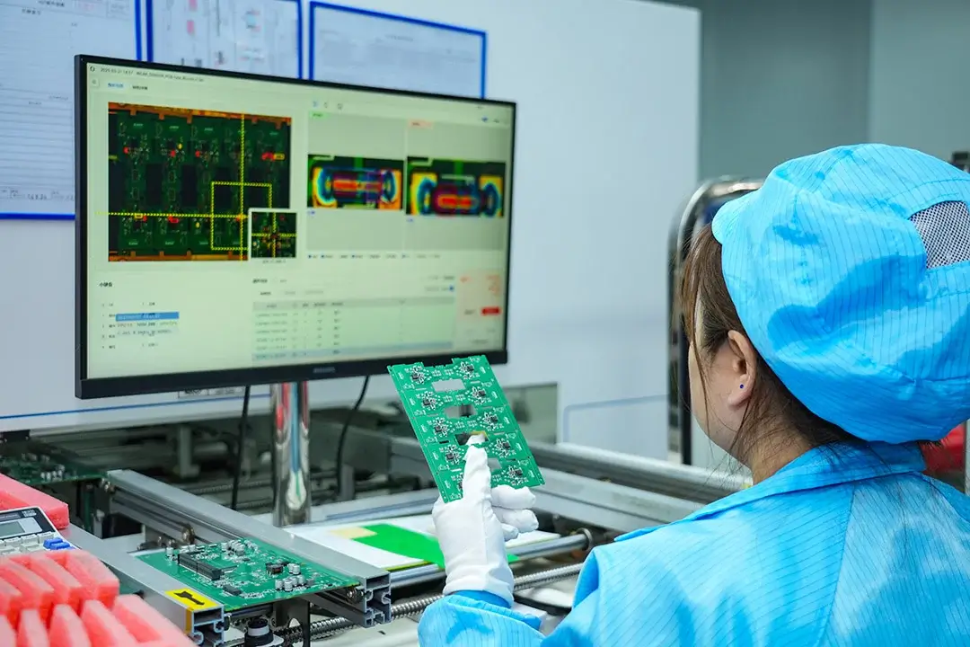
In conjunction with the assembly specifications, IPC-A-610J is used to determine the acceptability of the identified product class. The workmanship class and assembly drawing provide the inspector with a basis for determining the correct assembly configuration and whether it meets the visual acceptance criteria defined in IPC-A-610J. Therefore, IPC-A-610J visual acceptance criteria alone are not sufficient to verify an incorrectly populated PCB component location.
J-STD-001J provides soldering material, process-control, and acceptance requirements and is used in conjunction with SUGA's assembly specifications, approved process, and product class; therefore, it does not replace IPC-A-610J visual acceptability criteria.
Product Acceptance Conditions
The assembly drawing defines geometry and revision, the BOM defines component identity, and the product class defines workmanship. In addition, an approved sample may define the expected product appearance.
PCB Visual Inspection Process and Inspection Records
| Phase | Controlled input | Inspection control | Recorded result |
|---|---|---|---|
| 1. Criteria definition | Drawing, BOM, revision, product class and documented limits | Match the inspection object to the governing criteria | Board- or lot-specific inspection basis |
| 2. Identity and handling | Part number, revision, clean area, ESD protection and inspection tools | Confirm identity and establish controlled handling | Board released for observation |
| 3. Viewing setup | Feature size, reflectivity, access angle and required detail | Set illumination, field of view and magnification | Repeatable optical condition |
| 4. Area inspection | Whole board, defined zones, components, joints and mechanical features | Scan in a fixed order and classify visible conditions | Conforming area or located nonconformity |
| 5. Nonconformity capture | Board ID, feature location, image and applicable limit | Assign defect identity and preserve the observed condition | Traceable defect entry |
| 6. Correction closure | Corrective work and reinspection condition | Reinspect the same feature and assign any additional test | Accepted, corrected or transferred to further verification |
How Is Inspection Coverage Defined?
Coverage must clearly specify the inspected population and feature set; for example, incoming sampling, first article inspection, 100% board inspection, 100% programmed-feature coverage, or inspection focused only on defects that occurred or could have occurred after reworking the assembly. The term "100% AOI" refers only to the inspection of every feature included in the approved program; it does not mean that every solder interface is optically visible. The inspection documentation typically contains information about the revision, board side, panel position, sampling rule, programmed feature set, areas excluded or obstructed, and all locations transferred to manual inspection, X-ray, electrical testing, or functional verification.
Inspection Criteria and Board Identity
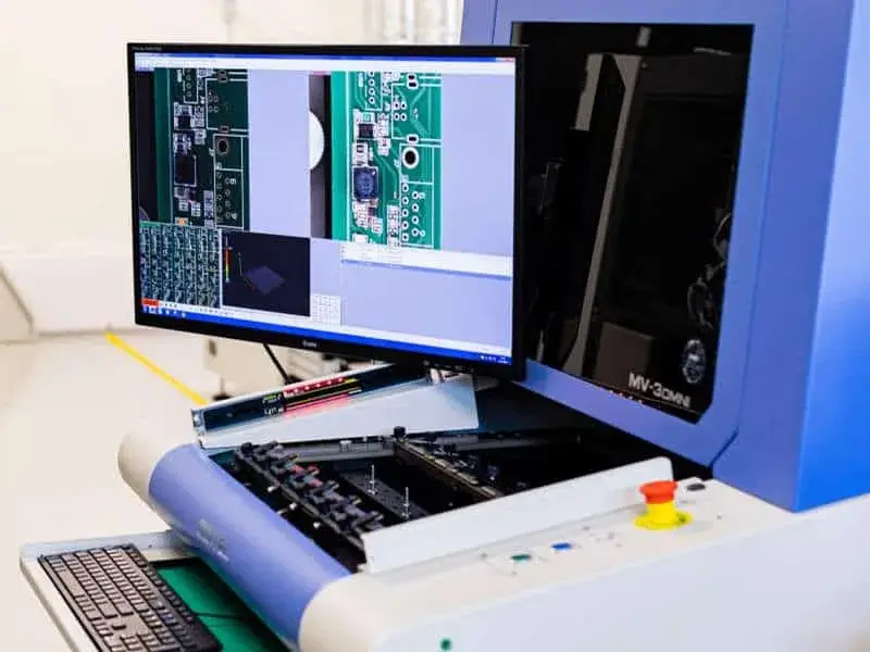
Criteria for bare boards are not applicable to assembled features, and boards with obsolete revisions cannot support a current product decision. The product part number, revision, panel position, and assembly documentation must match before a board or lot is released for use.
Maintaining a clean environment while handling assemblies helps prevent loose debris from being mistaken for a product defect. In addition, proper ESD controls protect the assembly from damage while it is being repositioned. Before visual scanning continues, SUGA establishes the clean-area requirements, handling methods, and inspection-tool status.
Inspection Sequence Across Board Areas
A fixed scanning order prevents the accidental omission of areas and makes it possible to compare results from previous inspections with the current inspection. The scanning process starts by inspecting the whole board to determine its identity and overall condition, then proceeds by board side, panel position, and defined zone. In each zone, scans become progressively more detailed, starting with the designators, accessible leads and joints, mechanical features, and finally cleanliness or revision markings. When preparing to reinspect, inspectors retain the same location reference used during the first inspection.
Defect Records and Reinspection Results
Usable defect records contain information regarding the board, revision, defect ID, designator or coordinate, defect image, observed condition, applicable criterion, disposition, corrective action taken, and reinspection result. One typical example of a usable defect record would state: Board A2317, Rev C, U14 pin 6, image VIS-042, visible solder bridge, bridge removed, same location reinspected, affected net passed short-circuit verification. The initial observation and final quality decision are recorded separately.
Reinspection occurs at the same location and under the same criterion as the first inspection. If there is a visible conductor gap, continuity verification is performed when circuit state must be confirmed; if there is a copper or solder bridge, short-circuit testing is performed; if a package interface cannot be visually verified, X-ray may be required; and if a functional area has been corrected, powered retesting may be required. The final inspection report retains the visual result and any additional test result as separate decisions.
PCB and PCBA Visual Inspection Areas
| Feature / location | Acceptance signal | Engineering response |
|---|---|---|
| PCB substrate | No visible delamination, blistering or warping | Hold the board or lot and assess the affected area against the applicable criterion |
| Board edges | No burrs, nicks or cracks outside documented limits | Hold the affected board and compare edge damage with the drawing or acceptance limit |
| Holes and vias | Visible hole openings are unobstructed and free from debris, surface damage or obvious registration anomalies | Measure hole geometry or inspect internal plating when the decision depends on size or hidden structure |
| Traces and pads | No lifting, peeling, oxidation, visible gap or unintended copper connection | Measure conductor geometry; use electrical testing to confirm opens or shorts |
| Solder mask | Aligned, adherent and clear of required contact areas | Compare mask alignment, adhesion and exposed-contact clearance with the documented limit |
| Silkscreen and polarity marks | Legible, aligned and consistent with the current revision | Resolve marking, identity or polarity conflict |
| Surface cleanliness | No foreign material, residue or handling contamination that violates the documented cleanliness requirement | Clean or segregate the affected board, then reinspect the same area |
| Bare-board identity | Part number and revision match controlled documents | Stop inspection and resolve the identity mismatch |
| Component population | Part, location and polarity match the BOM and assembly data | Correct the population error or hold the assembly for BOM or AVL review |
| Component position | Body and terminations remain within placement limits; no tombstoning | Rework the placement or hold the assembly when the applicable limit is exceeded |
| SMT termination alignment | Terminations align with pads within the applicable criteria | Compare centering and overhang with the applicable criterion; rework if nonconforming |
| THT seating / standoff | Seating and spacing match the assembly specification | Correct seating or standoff when it exceeds the assembly requirement |
| IC pins / fine-pitch leads | Accessible leads are straight, seated and undamaged | Use X-ray, electrical test or another specified method for inaccessible contacts |
| External solder joint | Shape, wetting, fillet and surface condition meet process limits | Correct the external nonconformity and reinspect |
| Solder bridge | No unintended solder connection between adjacent conductors | Remove the bridge, reinspect the joint and perform short-circuit verification when the affected network requires it |
| Solder debris | No loose solder balls, splashes or webbing | Remove contamination and reinspect the affected area |
| External solder anomaly | No pinhole, crack or exposed interface outside the applicable limit | Use X-ray or another structural method when the anomaly may extend beneath the package or joint |
| Mounting / hardware features | Correct location, clearance and freedom from obstruction | Remove the obstruction or hold the assembly for mechanical review |
| Jumpers / manual modifications | Approved, secure and consistent with the current revision | Resolve undocumented or incorrect modification |
| Connectors / mechanical integrity | Fully seated and free of visible cracking, looseness or damage | Hold the assembly and inspect seating, locking features and electrical function as required |
| Final configuration | Correct revision, cleanliness and completed visible inspection | Record visual release separately from any required electrical or functional retest |
Bare Board Features
Inspection of the bare board solely serves as an indicator and does not by itself verify dimensional or electrical nonconformance. The inspection process shows where the defect is located and its visible condition, while verifying whether that defect falls outside accepted dimensional or electrical specifications is done by measurement or electrical testing. Two visually similar findings may be located in the same area on the bare board, for example, roughness around a hole edge, but one may be determined as acceptable while the other is unacceptable. The visual data and subsequent decision regarding a particular bare-board defect should therefore be recorded as separate linked entries rather than as one final result.
Component Placement
The BOM, assembly drawing, polarity data, approved alternate components, modification log, and configuration checklist provide confirmation of a physical assembly’s configuration. While visual access allows confirmation of component placement, including population, orientation, seating, and alignment, visual identification of a compatible body outline or top marking on a component does not confirm the approved value, tolerance, voltage rating, or AVL source. Where component identification cannot be confirmed visually or is ambiguous, the components will need to undergo material and traceability verification.
Solder Joint Inspection
Visual inspection allows determination of accessible external wetting, fillet formation, solder bridges, contaminants, and solder-joint cleanliness. The external appearance of an assembly may be acceptable based on a top view, but the interface beneath a BGA, shield, connector, or bottom-terminated component cannot be determined visually. Assemblies with obscured interfaces must be analysed using X-ray or another approved method for verification.
Final Assembly Condition
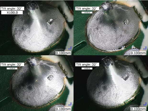
Closeout inspection confirms that the assembly configuration is correct and that no externally visible mechanical or workmanship defects are present. However, visual closeout inspection cannot confirm that the circuit performs or that a repaired net is restored. Assemblies with undocumented modifications cannot be closed out, even when they appear acceptable, until the modification is documented. Recording the visual inspection result and any required retest as separate linked decisions will ensure that assemblies are not released when they fail to meet the acceptance plan.
Visible Bare-Board Defects
Visual inspection allows identification and location of an external bare-board defect, but it does not confirm hole diameter, conductor spacing, internal plating, or complete circuit condition. Consequently, each defect description should differentiate between the observable signal and the measurement or electrical test required to determine the disposition of the defect.
| Defect | Observable signal | What visual inspection proves | Required next check |
|---|---|---|---|
| Breakout | Annular ring or hole edge is visibly broken out | External breakout is visible; dimensional acceptance still follows the applicable criterion | Compare the breakout and remaining annular ring with the bare-board criterion |
| Pinhole | Small visible hole or pit in conductor or coating | External surface anomaly is visible | Magnify the area; measure or evaluate the feature when size affects acceptance |
| Open-pattern indication | Visible gap in a conductor | The external gap is visible; continuity remains an electrical result | Perform continuity testing when the network decision depends on circuit state |
| Under etch | Excess copper remains around the intended pattern | External etch geometry is visibly abnormal | Measure conductor geometry against the drawing or applicable criterion |
| Mouse-bite | Repeated notches along a conductor edge | The conductor-edge anomaly is visible | Magnify and compare the notch geometry with the applicable limit |
| Missing conductor | Required copper feature is visibly absent | The missing external pattern is visible | Verify continuity or network state electrically when required |
| Spur | Unintended copper projection extends from a conductor | The copper projection is visible | Measure remaining spacing to adjacent conductors |
| Short-pattern indication | Visible copper connection joins conductors | The external connection is visible; complete circuit state remains electrical | Perform short-circuit or net testing |
| Wrong size hole | Hole appears inconsistent with the specified geometry | The visual discrepancy is visible; diameter still requires measurement | Measure hole diameter and compare it with the drawing |
| Conductor too close | Visible spacing appears below the intended geometry | The spacing concern is visible | Measure conductor spacing against the documented limit |
| Spurious copper | Unintended copper remains on the board | The external copper anomaly is visible | Remove it if it is loose contamination; otherwise compare the feature with the criterion |
| Large unintended copper connection | Broad unintended copper connection bridges patterns | A severe external pattern anomaly is visible | Hold or reject the board, then verify affected nets electrically |
| Missing hole | Required hole is visibly absent | The missing external feature is visible | Hold the board and verify the drawing and revision before disposition |
| Over etch | Excess copper removal narrows or breaks the conductor | External over-etch geometry is visible | Measure conductor width and test continuity if narrowing may affect the net |
Component Placement and Mechanical Defects
Actionable placement defects can only be identified if the required component states are understood first. Empty locations, incorrect designators, polarity reversals, shifted body positions, tombstoned components, bent leads, or poorly seated connectors can all be tied back to an image and board coordinates.
Visible Assembly Defects
Visible assembly defects include solder bridges, insufficient external wetting or fillet formation, lifted lands, exposed copper, solder debris, prohibited residue, other foreign materials, or mechanical damage. The inspection record documents the exact location of each defect and indicates whether the defect was reworked, accepted according to documented criteria, or transferred to X-ray, electrical testing, or functional retest.
PCB Visual Inspection Tools and Viewing Conditions
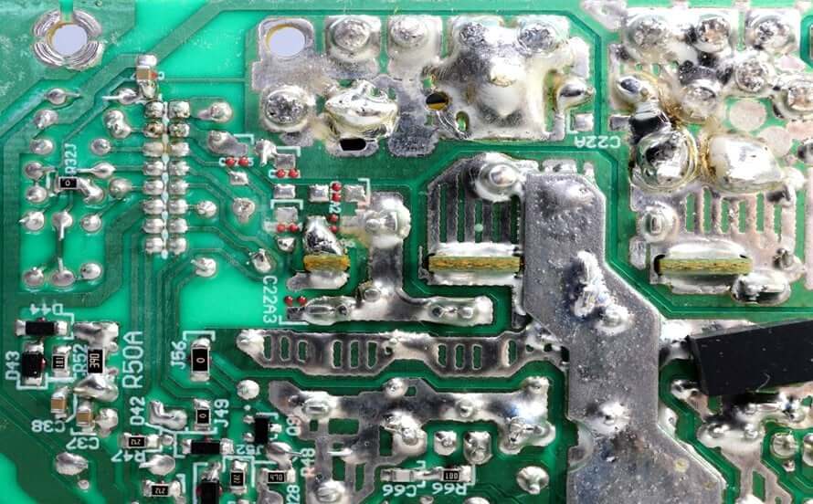
Maximum magnification of a PCB is not the goal when selecting inspection tools. Use the right inspection tools to identify the acceptance features of a board while maintaining enough context to locate them on the PCB and create reproducible evidence for traceability.
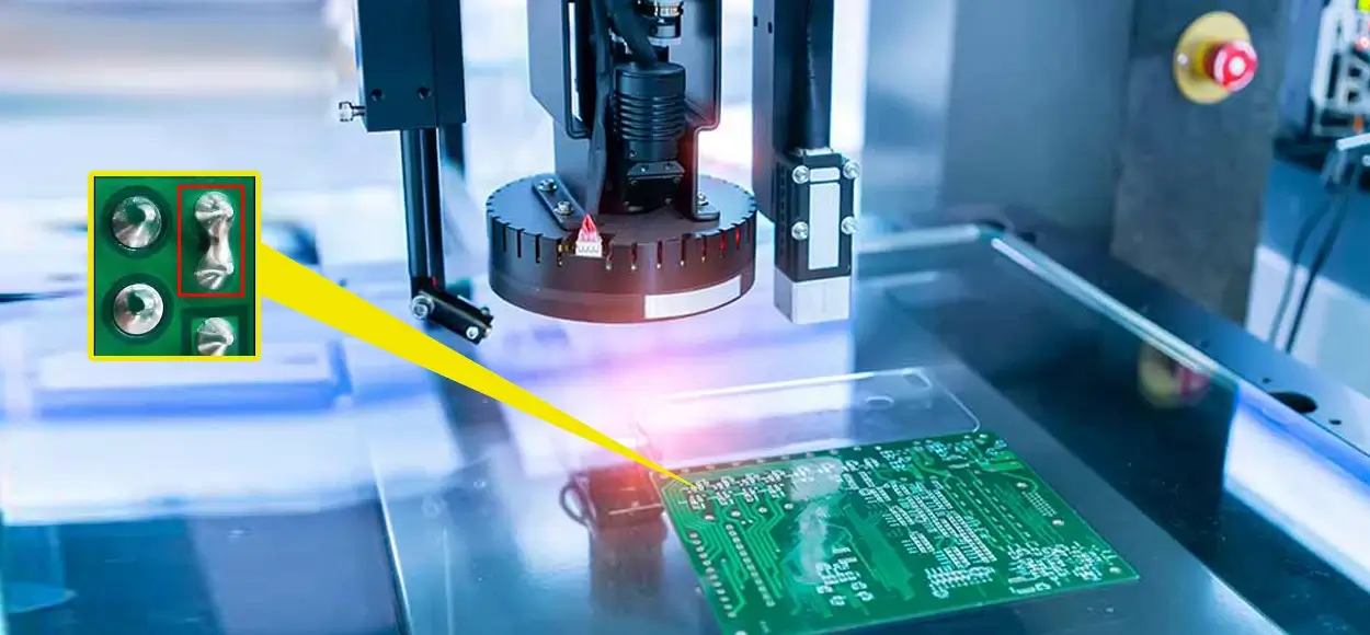
SUGA considers many factors when configuring inspection tools, including lighting configuration, feature-specific magnification, inspection cameras, and 2D or 3D AOI, based on feature size, surface reflectivity, board geometry, and optical access. Therefore, the selected inspection method must resolve the acceptance feature while maintaining board-location context and providing visible evidence for identification.

Lighting and Workspace Control
To identify an acceptance feature, the operator must adjust the angle, diffusion, and intensity of the light so that glare and shadows do not obscure the feature. Keeping the board in the same position allows comparisons and reinspections of the same area.
Dust and other loose debris that may be present on the workbench should be removed before inspection to prevent false defect detection. Proper ESD control measures protect assemblies from damage during handling, while a clean optical path prevents dust or dirt on the lens from interfering with image capture.
Selecting Magnification for the Feature
SUGA selects the lowest possible magnification that resolves the acceptance feature while providing sufficient useful context for PCB inspection. Acceptance features such as small pads, fine-pitch leads, fillets, mask edges, and conductor details typically require more magnification than a whole-board identity check.
Field of view and depth of field decrease as magnification increases. Therefore, magnification should only be increased when feature size, optical access, or acceptance detail requires it.
Cameras and Evidence Capture
The inspection process using cameras provides an image that aids in the classification, comparison, and reinspection of visible features. Images obtained during inspection must include the feature, its board location, and enough surrounding detail to associate the feature with a defect ID, including the scale or optical settings used when size affects the inspection decision.
2D or 3D AOI compares programmed features against approved references and identifies alarm locations. Program quality, image access, thresholds, and false-call handling determine how those alarms become production decisions.
Manual PCB Inspection vs. Automated Visual Inspection
Although production volume is important, product maturity and revision stability are more important. The manual and AOI inspection cycles must include the entire decision-making process, including setup, alarm confirmation, and record retention. Alarms generated by automated machines remain unconfirmed until they are classified by inspection personnel.
| Selection factor | Manual inspection | Automated optical inspection |
|---|---|---|
| Product state | Prototypes, low volume, frequent revision or variable visible conditions | Stable revision with programmable, repeated visible features |
| Repeatability basis | Work instruction, training, viewing control and inspector consistency | Program coverage, image quality, thresholds and alarm classification |
| Complete cycle | Board-complexity-dependent inspection time | Programmed scan plus alarm confirmation and handling |
| Cost structure | Inspector time, optical equipment and traceability depth | Program creation, changeover, imaging, false-call handling and data integration |
| Revision change | Instructions can be updated quickly | Image models, thresholds and coverage settings require update |
| Coverage pattern | Flexible judgment across accessible visible conditions | Repeatable programmed comparison of defined visible conditions |
| Alarm handling | Inspector classifies the observed condition directly | Machine alarm requires human confirmation and final classification |
Manual Inspection Strengths and Limits
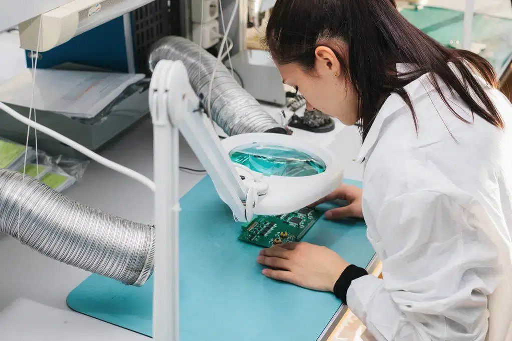
The inspector can change the viewing angle, magnification, and scan path depending on what is visible at the time of inspection. The inspector can exercise human judgement in situations where the inspected feature does not match stable image rules or when any area of the board requires particularly careful inspection.
The flexibility of manual inspection is determined by having clear inspection instructions, properly trained inspectors, and controlled viewing conditions. Therefore, as the number of inspected features and board complexity increase, inspector fatigue will reduce repeatability; hence, it is essential to have consistent decision rules and accurate zone-by-zone records for all inspected features.
How Are AOI False Calls Controlled?
AOI uses repeatable imaging to generate a production decision through program setup, image models, thresholds, and alarm classification. The first step in setting up an automated visual inspection program is determining which optically accessible features will be compared. The camera provides image quality based on the imaging setup, while the thresholds determine whether an alarm is triggered. Inspection personnel must then review the image to validate and classify the visible condition.
To control false calls successfully, the AOI system must prevent overly sensitive thresholds from burying relevant findings and prevent weak thresholds from leaving defined conditions outside detection. Hence, SUGA tracks confirmed results instead of initial alarm counts.
Production Volume and Changeover Tradeoffs
When program settings, image models, thresholds, and the visible feature set remain the same across repeated production runs, the setup becomes more economical. The approved program must remain linked to the current PCB and assembly revision. The comparison includes program creation, changeover, alarm classification, and data integration rather than only the equipment scan time.
Manual or mixed inspection remains applicable where there are frequent revisions or visible conditions that require inspector judgement. During stable runs, repeatable features can be placed under AOI. However, manual inspection must cover areas that AOI cannot see, such as obstructions, tall components, or atypical findings outside the programmed feature set.
PCB Visual Inspection Applications
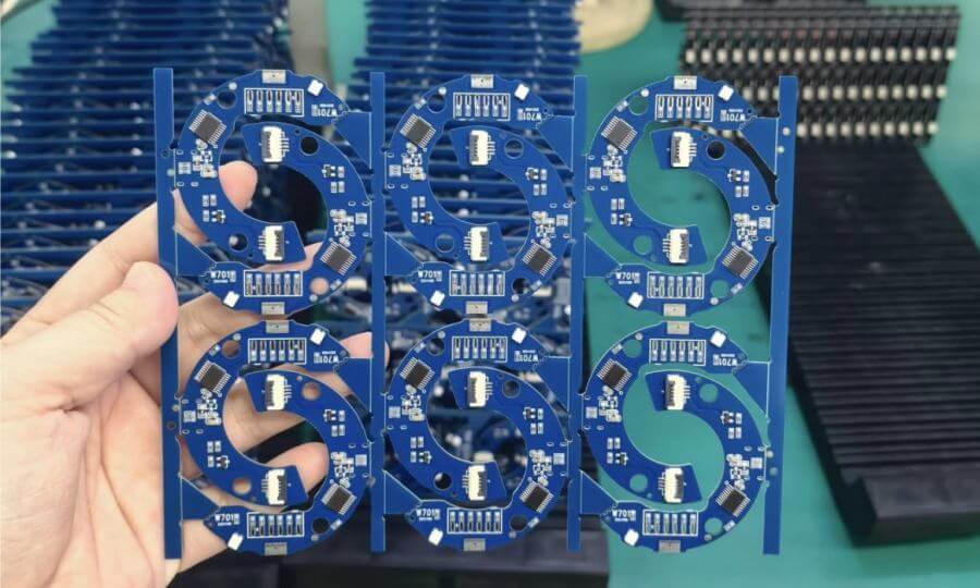
Bare PCB Incoming Inspection
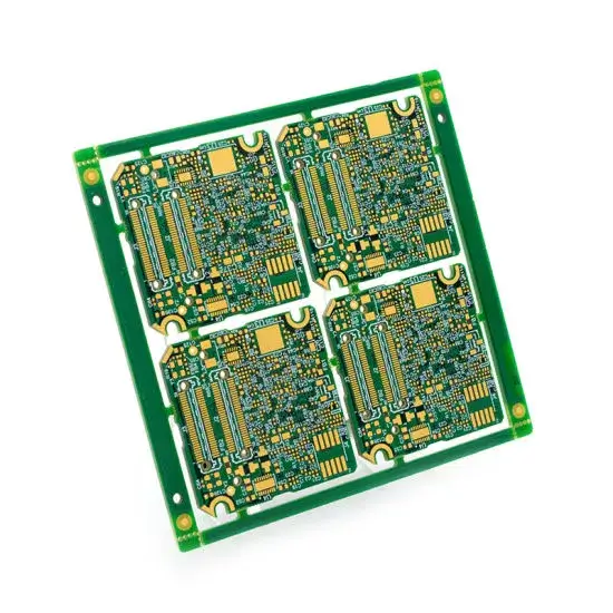
SUGA performs several checks to identify the board, confirm the PCB revision, locate the PCB panel position, check surface condition, edges and hole openings, and confirm that the solder mask and silkscreen have been printed to the specified requirements. Visual inspection also identifies visible damage or conflicting markings before printing or component placement. Through panel-position records, the visual inspector can distinguish a fabrication defect from one caused by scoring, depaneling, or transport. However, visual inspection cannot determine hole diameter, internal plating, buried defects, or electrical continuity, so those conditions must be validated through physical measurement, structural inspection, or electrical testing.
First-Article PCB Assembly Inspection
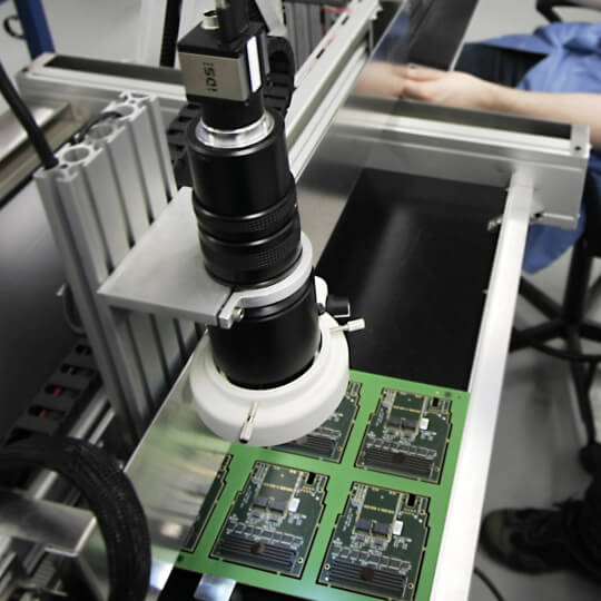
First-article inspection checks component presence, orientation, placement, connector seating, accessible solder joints, cleanliness, and approved manual changes against the BOM and drawing. Approved alternates must also be separated from unauthorized substitutions. If any conflicts arise involving polarity, component identity, assembly data, or AOI revision, the conflict will stop batch release. The first article can additionally support AOI program validation before automated inspection is used for continued production.
Prototype and Low-Volume Inspection
Prototype and low-volume assemblies tend to have numerous ECOs, manually performed modifications, and limited reference samples. In most instances, inspectors compare each board against the current BOM, drawing, polarity data, ECO, and modification records. If any jumpers or manual changes are undocumented, they will not be accepted based on workmanship alone. After repeated rework on an individual assembly, the inspection focus shifts to lifted pads, damaged solder mask, remaining solder contamination, disturbed adjacent components, and revision mismatches at the affected designators.
Repeated SMT Production
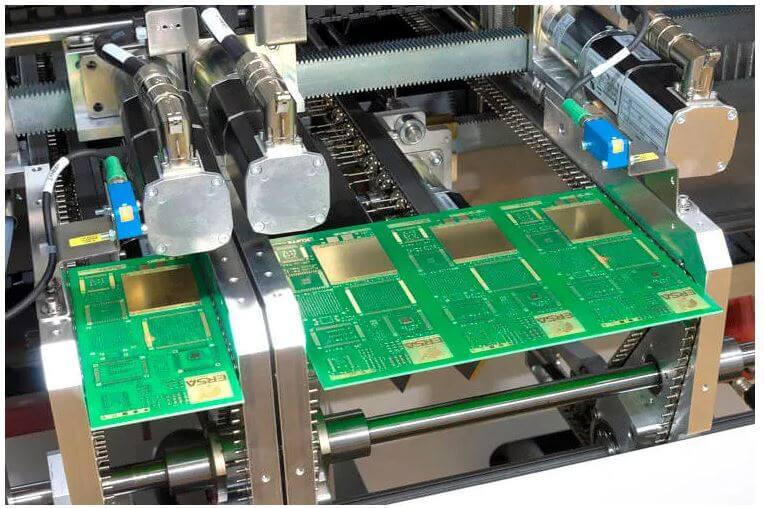
For stable SMT production, AOI provides repeatable inspection of production boards for missing components, shifting, tombstoning, polarity errors, and accessible solder conditions. The inspection program must match the PCB currently in use, along with the BOM and assembly revision. An outdated image model may repeatedly approve incorrectly assembled products or reject approved changes across a batch. Confirmed defect results, program-to-revision linkage, and changeover verification therefore control production actions rather than raw alarm counts alone.
Through-Hole and Mixed-Technology Assemblies
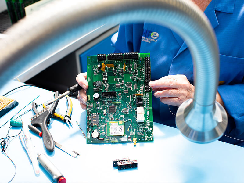
Through-hole and mixed-technology boards require separate inspection views for component seating, standoff, polarity, locking features, lead position, and solder-side fillets. Tall connectors, transformers, and mechanical parts can block AOI camera access, requiring SUGA to use targeted manual inspection for shadowed areas and interference risks. Visual inspection confirms accessible features, but electrical or functional testing is required to determine internal connector contact, full connector engagement, electrical continuity, and load performance.
Final Assembly and Rework Verification
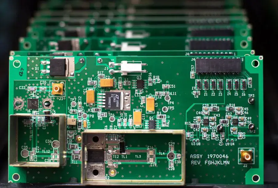
Final and post-rework inspection examines the repaired designator and surrounding area for lifted pads, damaged solder mask, solder splash, residue, disturbed adjacent components, approved jumpers, connector seating, mounting features, revision identity, and cleanliness. Because heat used during rework can affect adjacent components or joints beyond the original repair location, visual acceptance and electrical or functional retesting remain separate results. Restored appearance does not confirm circuit performance.
Additional Verification After Visual Inspection
How Are Concealed Interfaces Examined?
Package bodies, shields, and connectors obstruct the optical path, which prevents the inspector from photographing or examining what lies beneath them. Visual inspection verifies placement, accessible leads, surrounding solder, contamination, and external damage around these features. For example, a package perimeter could appear clean and undamaged; however, this does not prove a sound physical joint beneath the package. Voiding, head-in-pillow, and similar conditions are not visually detectable; they fall under the category of structural findings, which must be verified using X-ray or another accepted structural verification method.
Electrical Verification After Visual Inspection
Electrical testing following visual inspection is conducted when the decision depends on the circuit state of a conductor gap, unexpected copper connection, or corrected solder bridge identified by location. The electrical test verifies actual circuit conditions, including an open, short, or restored working net, based on electrical results rather than visual evidence. Locations that pass visual inspection do not have to be retested electrically unless the acceptance plan specifies otherwise. The visual and electrical results remain linked to the same location and defect ID but are recorded as separate decisions.
Functional Verification After Visual Inspection
An external evaluation looks at component condition, accessible solder workmanship, mechanical integrity, cleanliness, and revision identity. Functional verification evaluates input and output response, timing relationships, interface behaviour, and performance under specified loads.
Frequently Asked Questions
Bare PCB inspection looks for fabrication features such as edges, holes, conductors, pads, solder mask, silkscreen, and surface condition before components are attached. PCBA inspection looks for component presence, orientation, placement, accessible solder joints, connectors, overall cleanliness, and approved modifications against the BOM and assembly drawing.
Visual inspection can confirm package position, accessible leads, external fillets, surrounding solder, contamination, and visible damage. Visual inspection cannot verify the condition of solder interfaces beneath BGA packages, shields, connectors, or other blocked features. To determine whether voiding, head-in-pillow, or another concealed condition is present, X-ray or another structural inspection method must be used.
Manual inspection is used for prototypes, low-volume production, frequent revisions, approved variations, tall components, connectors, and through-hole features that require flexible viewing angles or inspector judgement. For stable assembly revisions where the same visible features can be programmed consistently, AOI is more suitable. However, most assemblies use both forms of inspection to accommodate differences in optical access and product maturity.
When using a qualitative inspection tool, it is essential to check clean optics, stable lighting, focus, and documented service status. When a camera or microscope is used for size-based acceptance, the tool should have a verified scale or measurement system. AOI requires program validation, optical verification, and maintenance under the quality system. The calibration or verification interval depends on equipment specifications, use, drift history, and internal procedures; a single interval cannot be established for all visual inspection tools.
The primary difference between 2D AOI and 3D AOI is that 2D AOI inspects two-dimensional surface images, while 3D AOI also provides height information. Height information is relevant for raised features or coplanarity conditions. Shadows, reflections, optical access, program complexity, and false-call confirmation can affect both types of inspection. The geometry of the PCB and the features being inspected determine whether 3D AOI provides useful additional evidence.
Factors that affect the total cost of PCB visual inspection include board quantity, panel format, inspected sides, number of components or features, first-article inspection, sampling or 100% coverage, required magnification or imaging, AOI program creation or modification, alarm confirmation, image retention, defect reporting, and post-rework reinspection. Hidden-joint X-ray, electrical verification, or functional retesting are separate cost drivers when visual inspection cannot close the decision.