Upload BOM & Gerber
-
Mobile: +86 13312967631
-
Email: sales@sugaintl.com

3D Automated Optical Inspection
PCB Assembly Supplier with 3D AOI and Inline Process Feedback
Deploy 3D AOI at selected inspection points after component placement, reflow, or later assembly, then connect confirmed geometry defects to board disposition, repair, and verified process correction.
2 Inline AOI Stages
16 Programmed Defect Conditions
6 Requalification Triggers
3D Height & Coplanarity
What Is 3D Automated Optical Inspection?
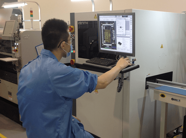
3D AOI utilizes a non-contact machine-vision process to build a three-dimensional model of the visible surfaces on PCBs and PCBAs, which then aids in determining the physical location of an object on the PCB, including its position, rotation, height, tilt, and coplanarity, while also evaluating accessible solder geometry. 3D AOI captures the surface of the PCB or PCBA, maps data points to board coordinates, and compares these coordinates with the locations of parts indicated by an approved reference.
What 3D AOI Measures
3D AOI measures all programmed locations of each part or feature, which are then compared with the approved locations for that part type. The program compares X/Y position, Z-height, angle, area, contour, and coplanarity against qualified limits. These measured data points can then be reported as a defined deviation from the programmed reference, with the associated board location, image, and inspection program revision documented.
The inspection program can evaluate visible component presence, polarity, position, seating, lead geometry, exposed solder features, local board-plane variation, visible residue, and foreign material when optical access, resolution, and controlled reference data support the decision.
Assembly Process Control
SUGA utilizes 3D AOI as a process-control method in PCB and PCBA manufacturing. Our team creates and validates all inspection programs, confirms machine calls, determines board action, reinspects repaired assemblies, implements corrective actions for recurring placement or process issues that affect multiple boards, and maintains accurate records for each board or assembly throughout the manufacturing process.
Three-Dimensional Measurement Principles
A reliable 3D AOI decision depends on four linked controls: stable optical capture, coordinate registration, surface reconstruction, and a qualified local reference. Changing the support from one board to another, changing the fiducial registration, changing the component finish, or changing the type of lighting can make the same physical feature produce different measured heights or contours; therefore, all four controls must be qualified together.
Lighting and Depth Capture
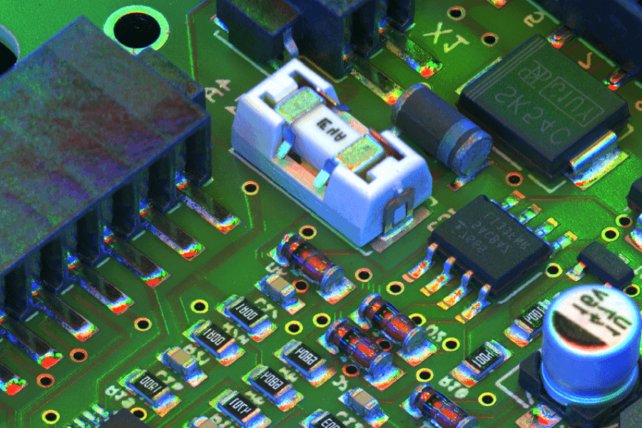
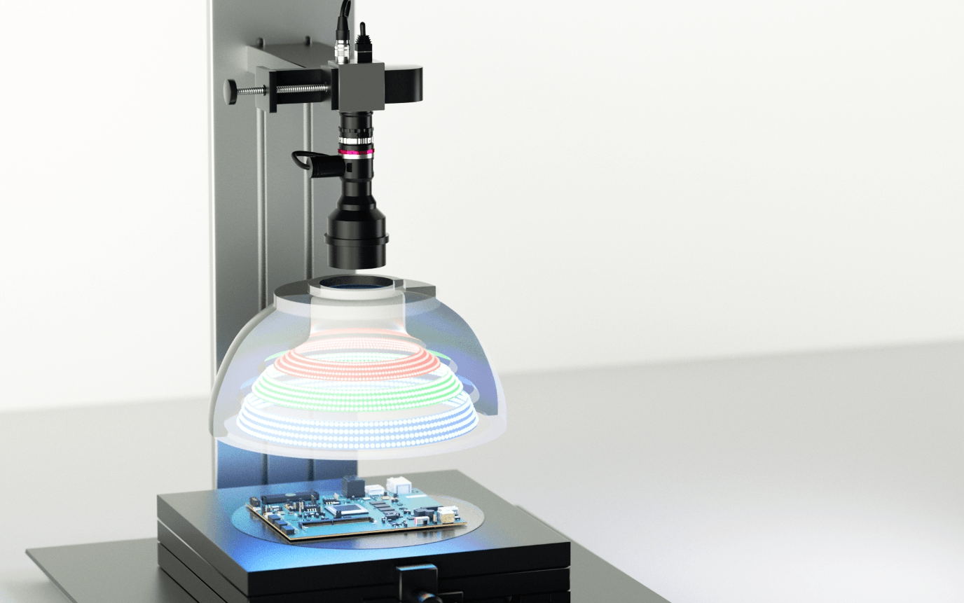
Lighting and depth capture use different types of illumination to generate different reflections from solder joints, package bodies, package markings, solder mask, and substrates; therefore, selecting the appropriate wavelengths and exposure settings improves feature separation when measuring surface conditions and visible solder joints. Depending on how the AOI platform for the assembly line has been designed, depth data may be extracted using phase-shift imaging, structured illumination, laser profiling, or calibrated multi-view imaging; therefore, to generate a qualified recipe for the actual board finish and component population, the recipe must match the AOI platform’s depth-capture method.
Coordinate Registration
Coordinate registration creates a link between the calibrated camera position, calibrated illumination, fixed stage movement coordinates, and board height calibration. The combination of fiducial locations and programmed board features allows each view to be converted to a common board coordinate system; thus, the captured signals are combined to create a height profile or an equivalent three-dimensional representation.
Glare, shadows, low-contrast markings, visible residue on the PCB surface, vibration, board movement, or calibration drift can weaken the image captured by the camera. As a result, SUGA qualifies the lighting, exposure time, camera angle, focus, feature region, and image reconstruction settings for the actual PCB revision and component population. The threshold setting is not adjusted merely to hide an unstable image; rather, the correct capture condition must be established before adjusting the threshold settings.
Local-Plane Measurement
In local-plane measurement, the captured data is analyzed by comparing the reconstructed profile with a local plane or another programmed datum reference. Because the reference is local, the method separates component seating from underlying board-plane variation and prevents a global height reference from distorting the result. It can determine whether a component is acceptably seated relative to the local reference surface or only appears high in the global PCB coordinates because adjacent PCB surfaces are bowed.
Approved Gerber or CAD files, centroid coordinates, assembly drawings, component libraries, polarity definitions, package geometry, and known-good or first-article boards provide the programmed reference for determining component position, angular offset, body height, lead height, tilt, coplanarity, visible area, and surface shape, as well as calculated profile or volume values.
Machine Call Confirmation
When a measured value exceeds the programmed limit, a machine call is generated linking the board, coordinate, feature, image, and program version used. Confirmation determines whether the call represents an actual defect, an allowed variation, or an optical or program false call before board action and traceability are assigned.
2D vs. 3D AOI
| Decision Field | 2D AOI Evidence | 3D AOI Added Evidence | 3D AOI Selection Trigger |
|---|---|---|---|
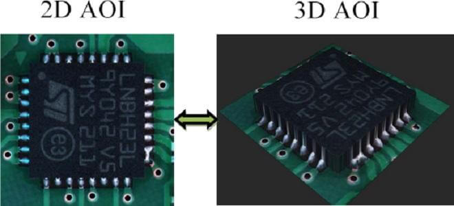
| Imaging basis | Planar intensity, color, edge, marking, and X/Y data | Height map or reconstructed surface shape | Use 3D when Z-height or surface shape changes the decision |
| Defect signal | Visible planar surface difference | Height, angle, shape, and volume variation | Use 3D when planar appearance cannot separate accept and reject |
| Component checks | Body, marking, polarity, presence, orientation, and planar position | Body height, tilt, lead height, coplanarity, and surface profile | Use 3D for seating, lifted leads, tilt, or coplanarity |
| Measurement controls | Lighting, reference data, thresholds, and resolution | Calibration, optical access, reconstruction, reference data, and thresholds | Qualify the actual optical recipe, calibration, and threshold set |
| Solder-joint checks | Exposed color, area, edge, and planar shape | Exposed height, visible area, fillet contour, coverage, and surface profile | Use 3D when exposed fillet height or profile drives acceptance |
| Coplanarity | X/Y position and visible edge relationship | Direct height relationship for leads, terminals, connectors, and packages | Use 3D when direct height difference drives the decision |
| Output record | 2D image, planar measurement, and classification | 3D model or height map, geometry, image, and classification | Retain board ID, feature value, image, decision, and program version |
Where Is 3D AOI Used in Production?
The PCB assembly process includes an initial AOI station after components have been placed on the board, followed by another after the board has been reflowed. In addition, a final optical inspection station can be set up after later assembly operations, including through-hole insertion, selective soldering, hand soldering, or mechanical attachment, when these operations create new visible geometry. All measurements of solder-paste geometry are recorded before placement using 3D SPI.
3D SPI Before Component Placement
Before component placement, 3D SPI records the solder-paste geometry, including height, area, volume, position, and shape. 3D AOI later analyzes the assembled PCB to determine component placement, seating, and visible post-reflow solder geometry. The upstream solder-paste record allows variations in solder print height, area, volume, position, and shape to be identified before the component body covers the solder paste. Comparisons between the solder-paste geometry recorded by SPI before component placement and the geometry recorded by AOI after reflow can help an engineer distinguish solder-paste printing variation from placement or reflow causes without treating AOI and SPI as interchangeable.
If the same post-reflow solder-geometry condition is identified repeatedly on the same package type or pad pattern, the SPI record may indicate whether the solder-paste variation was present before component placement. If the SPI measurements are stable while the post-reflow solder geometry varies, the source of the variation may be component placement, component finish, or the thermal process that the assembly underwent rather than solder-paste printing.
Placement Inspection Before Reflow
For SMT production, AOI after component placement and before reflow can isolate issues related to component loading and placement before solder joints are formed. The AOI program can identify missing, extra, incorrect, reversed, shifted, rotated, standing, or on-edge components, along with excessive height, tilt, incorrect seating, and optically accessible coplanarity conditions.
Identifying a placement problem at this stage can prevent an assembly from entering reflow and can also provide visibility into ongoing issues associated with the feeder, nozzle, X/Y coordinates, rotation, package-library selection, or placement height. A confirmed pattern feeds directly into the pick-and-place program or responsible process setting. As a result, operators correct, hold, or otherwise disposition the board according to the applicable work instruction.
Post-Reflow 3D AOI
3D AOI is performed after the reflow process to inspect the assembled state produced by printing, placement, and thermal processing.
Although post-reflow 3D AOI can show repeatable patterns associated with printing, placement, material, or reflow conditions, the images alone do not prove the root cause of the repeated condition. Each machine call must still be verified against the physical board and the approved threshold values. For example, repeated bridges at one aperture, shifted bodies at one feeder position, or lifted leads after a specific thermal profile require different types of process evidence.
Final Assembly Inspection
Final 3D AOI or programmed optical inspection takes place after later assembly operations, including through-hole insertion, selective soldering, hand assembly, shield or connector installation, repair, and cleaning. A qualified program can inspect accessible component orientation, connector or relay seating, coplanarity, protrusion or assembly height, visible solder profiles, foreign material, and repair workmanship.
The order of inspections is important because some features will be hidden from view under shields, heat sinks, connectors, or enclosures after assembly. Therefore, these features should be inspected before any assembly operation that will conceal them. The final assembly inspection verifies the installed height, seating, protrusion, and visible workmanship of the added components or hardware.
SUGA establishes inspection points based on board structure, defect risk, optical access, production stage, and acceptance requirements.
What Defects Can 3D AOI Detect?
The 3D AOI software uses quantifiable and optically visible differences to identify defects instead of relying only on generic defect names. Each inspected feature is defined according to variables including package geometry, PCB surface finish, optical access, assembly stage, and accepted workmanship criteria. A defect call is based on the surface signal detected during inspection.
Component Placement Defects
The rules for component presence and position depend on a stable visual reference rather than only a presumed centroid. For example, packages can have the same physical dimensions but different electrical characteristics, while approved alternative packages may differ in body color, component-marking location, or polarity markers. Therefore, the AOI software maintains references for specific package variants and does not rely on footprint matching as proof of component identity. If no stable marking or package feature is visible, AOI can verify component presence and placement but cannot confirm the manufacturer part number.
Component Seating Defects
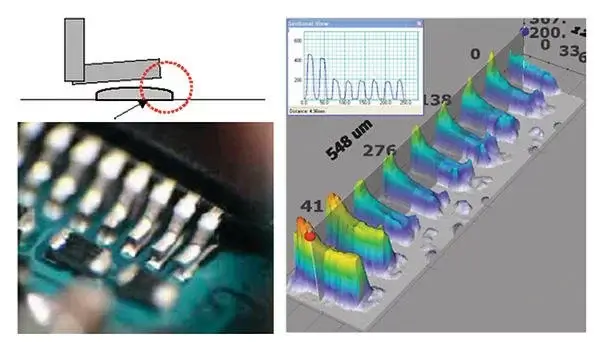
Genuine component-seating variation can be separated from PCB surface-plane variation by using height and angular relationships. A package may appear high in the global reference frame because the local PCB is bowed, while an individual lead may sit above the qualified lead plane even when the package body appears level. Although the AOI program measures geometry relative to the local plane, a measured lead height above the qualified surface does not necessarily indicate an electrical open. Electrical testing is still required to verify continuity.
Visible Solder Joint Geometry
3D AOI evaluates exposed solder-joint geometry rather than determining whether hidden wetting occurred beneath a component or covered termination. For example, solder joints may have a similar visible area while the concealed solder geometry beneath a QFN, BGA, or covered termination differs significantly. A visually acceptable fillet does not prove continuity. AOI software can identify consistent changes in exposed height, contour, surface coverage, bridges, isolated solder objects, or other visible solder inconsistencies and correlate those factors with SPI, placement, reflow, X-ray, or electrical test data as appropriate.
Board Surface Conditions
Board surface conditions can also be reconstructed using AOI data, allowing operators to identify local variation in the board surface, visible board deformation, and foreign material or debris detectable within the qualified optical resolution of the AOI system. Apparent deformation may also result from board support, conveyor clamping, or seating conditions. Any whole-board warpage conclusion requires the installed AOI system and datum method to be qualified. AOI cannot determine ionic cleanliness or identify the chemical composition of visible contamination.
| Defect Class | Defect Condition | 3D Decision Signal | Inspection Stage |
|---|---|---|---|
| Component position | Misalignment | X/Y, rotation, or 3D offset from the programmed feature | Pre-reflow placement AOI / post-reflow 3D AOI |
| Visible solder geometry | Solder-joint variation | Exposed height, visible area, fillet contour, coverage, or surface profile outside reference | Post-reflow 3D AOI |
| Component presence | Missing component | Expected body, lead, or marking feature absent | Pre-reflow placement AOI / post-reflow 3D AOI |
| Component identity | Incorrect component | Package or marking profile differs from the component library or reference | Pre-reflow placement AOI / post-reflow 3D AOI |
| Lead geometry | Lifted lead | Lead height, angle, or contact-plane relationship outside limit | Pre-reflow placement AOI / post-reflow 3D AOI |
| Component orientation | Tombstoning | One terminal elevated; component body standing on end | Post-reflow 3D AOI |
| Visible solder geometry | Solder bridge | Visible solder path between adjacent pads or leads | Post-reflow 3D AOI |
| Visible solder geometry | Insufficient solder | Exposed height, area, contour, or coverage below the qualified limit | Post-reflow 3D AOI |
| Board geometry | Board warpage | Local or global board plane outside the programmed reference | Assembled-board 3D AOI |
| Surface condition | Foreign-object debris | Unplanned 3D object or surface feature | Post-reflow / final 3D AOI |
| Component orientation | Polarity / reversed component | Polarity mark, body feature, or rotation conflicts with the reference | Pre-reflow placement AOI / post-reflow AOI |
| Component orientation | Billboarding | Chip body on side; abnormal body height or face orientation | Post-reflow 3D AOI |
| Visible solder geometry | Excess solder | Exposed height, area, contour, or coverage above the qualified limit | Post-reflow 3D AOI |
| Visible solder geometry | Solder balls | Isolated reflective 3D object near a pad, lead, or package | Post-reflow 3D AOI |
| Visible solder geometry | Visible open / incomplete joint | Expected exposed lead-to-pad contact or contour absent or discontinuous | Post-reflow 3D AOI |
| Component / board surface | Visible damage / deformation | Unexpected height loss, impact, or profile distortion | Final 3D AOI / manual confirmation |
3D AOI Program Development
AOI Reference Setup
- Ensure that Gerber or CAD files, BOM, centroid data, drawings, and revision identifiers agree with each other and describe the same released PCB or PCBA revision and manufacturing configuration.
- Define a list of designators and map their expected package or profile features to component-library records.
- For inspection, define the polarity, orientation, body, leads, connectors, and visible solder features.
- Define board alignment using fiducials and suitable local references.
- Define lighting, viewing, exposure, reconstruction, and measurement regions based on the actual finish and component mix.
- Create program versions based on the PCB or PCBA revision and approved manufacturing configuration.
The integrity of the references is as important as optical quality. If the BOM is incorrect, the coordinate file is outdated, the package library is incorrect, alternate parts are not controlled, or the revision is incorrect, false calls or false acceptance can occur even when both image capture and reconstruction processes are functioning properly.
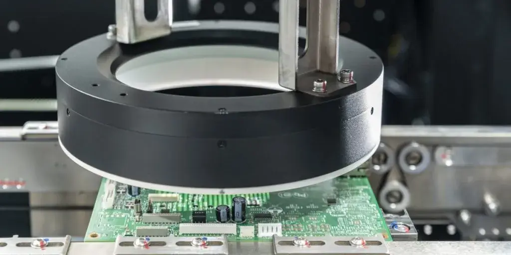
Threshold Qualification
An acceptance threshold converts a measurement into a decision window. SUGA places this window around the actual feature, workmanship requirement, process capability, and allowable product variation. An acceptance threshold that is too tight creates unnecessary false calls, while one that is too broad creates escapes. A single numerical limit is not applied uniformly to dissimilar package families where the geometry, finish, lead form, or optical response differs. Qualification can be established using first-article boards, known defect examples, engineering assessments, repeat scans, or correlation between inspection and testing results, as appropriate for each feature.
- Define acceptable tolerances for position, rotation, height, angle, coplanarity, area, volume, and visible contour for the selected feature.
- Document acceptable variations in component body, marking, solder finish, color, reflectivity, or supplier lot.
- Challenge the program using accepted boards and representative defect conditions.
- Record the setup and qualification basis of the accepted program version before repeat production.
- Align visual acceptance standards with approved product data, customer requirements, and IPC-A-610J acceptance criteria; align soldering process requirements with J-STD-001J.
False Calls and Escapes
False calls occur when an accepted visible condition is rejected, while escapes occur when a nonconforming condition is accepted or not called. They are evaluated independently because reducing false calls by loosening a threshold may increase escapes if the capture and reference problems are not resolved first.
- Analyze each false call, nuisance variation, and possible escape independently, and retain the accepted feature and qualification basis for each threshold.
- Test repeat-scan consistency for critical features and analyze false calls and confirmed escapes by defect family.
AOI accuracy is not one universal number. It depends on feature size, optical access, resolution, calibration, reflectivity, reconstruction quality, reference-data integrity, threshold design, and the defect population used for qualification. Therefore, false-call and escape performance should be reviewed by defect family, package type, AOI program revision, and qualification sample rather than compressed into one unsupported accuracy claim.
Program Requalification
The depth of requalification depends on what has changed. A change in component finish or color may affect only the optical recipe, while a moved fiducial, altered board outline, or change to the support condition may compromise registration and height decisions across a larger area.
| Change Trigger | Required 3D AOI Update |
|---|---|
| PCB or PCBA revision | Regenerate affected references; requalify changed features |
| Alternate component | Update library, recognition feature, lighting, and threshold |
| Package or lead geometry | Requalify position, height, angle, and coplanarity |
| Finish, solder appearance, or component color | Requalify lighting, exposure, contrast, and false-call rate |
| Stencil, placement, or reflow change | Requalify affected features; confirm the first article |
| Repair process or workmanship criteria | Update visible acceptance rules and reinspection records |
Traceable AOI Reports
Reports generated from traceable 3D AOI inspection can contain the following data:
- Production lot number and board or panel identification
- PCB/PCBA revision and 3D AOI program version
- Date and time, inspection station, and applicable line or machine identifier
- Component designator or board coordinate
- Defect category and machine call
- Captured inspection image, 3D view, and relevant measured value
- Human or engineering confirmation result
- Board action, repair history, and retest status
- Program or process correction when a repeated cause is identified
For panelized production, retaining both the panel ID and circuit position allows an individual failure at one physical location to be distinguished from a broader defect affecting a component or process. IPC-1782B can provide the traceability reference when required by the customer or product control plan. Engineers can review recurring AOI calls by component, coordinate, lot number, line, program version, or time period, determine the required correction or repair, and track the confirmed defect through correction, repair, and confirmation.
Inline AOI Process Control
SUGA uses inline 3D AOI as a closed loop. The process confirms the AOI call and determines board disposition, investigates repeated defect patterns, corrects the verified program or process cause, and confirms both the affected board and subsequent production.
Confirmed Defect Response
The confirmed defect response compares the AOI call with the physical board, approved reference, and measured value to determine whether the call represents an actual visible defect, acceptable feature variation, or an optical or program false call.
After confirmation, the board may be accepted, held for assessment, assigned to rework, sent for additional inspection or testing, or rejected. A one-time call controls the individual board; repeated calls are analyzed by component, feeder, coordinate, material lot, production line, or time window so the response also addresses the recurring pattern.
AOI Process Correction
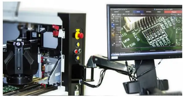
Patterns identified from repeated AOI calls initiate a focused review of component coordinates or rotation, feeder or nozzle condition, solder-paste deposition, placement height or force, reflow settings, material handling, and other manufacturing records associated with the defect. The responsible parameter is changed only after the AOI pattern has been correlated with physical evidence or applicable machine and process data. A defect pattern associated with a single inspection image does not, by itself, provide sufficient evidence to determine the actual root cause.
The AOI program is corrected when a library profile, optical recipe, component feature region, threshold setting, or classification criterion fails to separate accepted conditions from defective conditions. Work instructions and repair methods are also revised when they contribute to the cause. Program or process changes are versioned and confirmed before further processing of the affected component or associated product.
Correction Effectiveness
A repair is considered closed after the corrected feature passes the applicable 3D AOI reinspection. Any additional inspection or test performed on the repaired item remains linked to the original 3D AOI call and retest record.
SUGA evaluates confirmed defects and false calls by defect family, component, coordinate, lot, production line, and time window, then checks the expected measurement change or reduction in defect frequency during subsequent production. Correcting the defect closes the individual board record; however, the process action closes only after later inspections confirm that the recurring defect pattern has changed as expected.
3D AOI Inspection Limits
3D AOI Optical Access Limits
Conditions such as reflections, shadows, occluded lines of sight, visible residue, and incomplete reference data can prevent a stable optical decision. A feature that is not optically visible cannot be made visible through more aggressive or adjusted threshold settings. Covered terminations or connections cannot be observed by changing the AOI threshold. 3D AOI does not establish concealed joint geometry, electrical continuity, ionic cleanliness, or powered behavior unless a separate qualified inspection or test supplies that evidence.
| 3D AOI Condition | AOI Decision Basis | When AOI Is Not Enough | Required Confirmation |
|---|---|---|---|
| Exposed component or lead | Position; rotation; height; tilt; coplanarity | Feature must remain optically visible and separable; the lead or termination is obscured, or connection remains uncertain. | X-ray for concealed geometry; electrical evidence for connection |
| Bottom-terminated package | Package-body position; height; orientation; visible perimeter | Bottom solder joints are concealed; joint geometry affects acceptance. | X-ray of the concealed joint structure |
| Visible solder fillet | Exposed height; area; contour; coverage; surface profile | Does not establish concealed geometry, internal wetting, or continuity; hidden joint condition or circuit behavior remains in question. | X-ray and/or electrical or functional evidence as specified |
| Reflective or shadowed feature | Qualified lighting; multi-view capture; local reference | Surface signal is unstable or partially occluded; repeated false calls or incomplete reconstructed geometry remain. | Alternate optical recipe, viewing condition, or manual confirmation |
| Repaired assembly | Reinspection of the corrected visible geometry | Visible reinspection does not prove electrical or functional recovery when the repair affects connection or powered behavior. | Electrical or functional retest linked to the AOI repair record |
| New revision or alternate component | Updated library; feature region; reference; threshold | The previous program may not represent changed body, marking, color, height, or termination geometry. | First-article 3D AOI program qualification |
3D AOI Applications
Automotive Electronics PCB
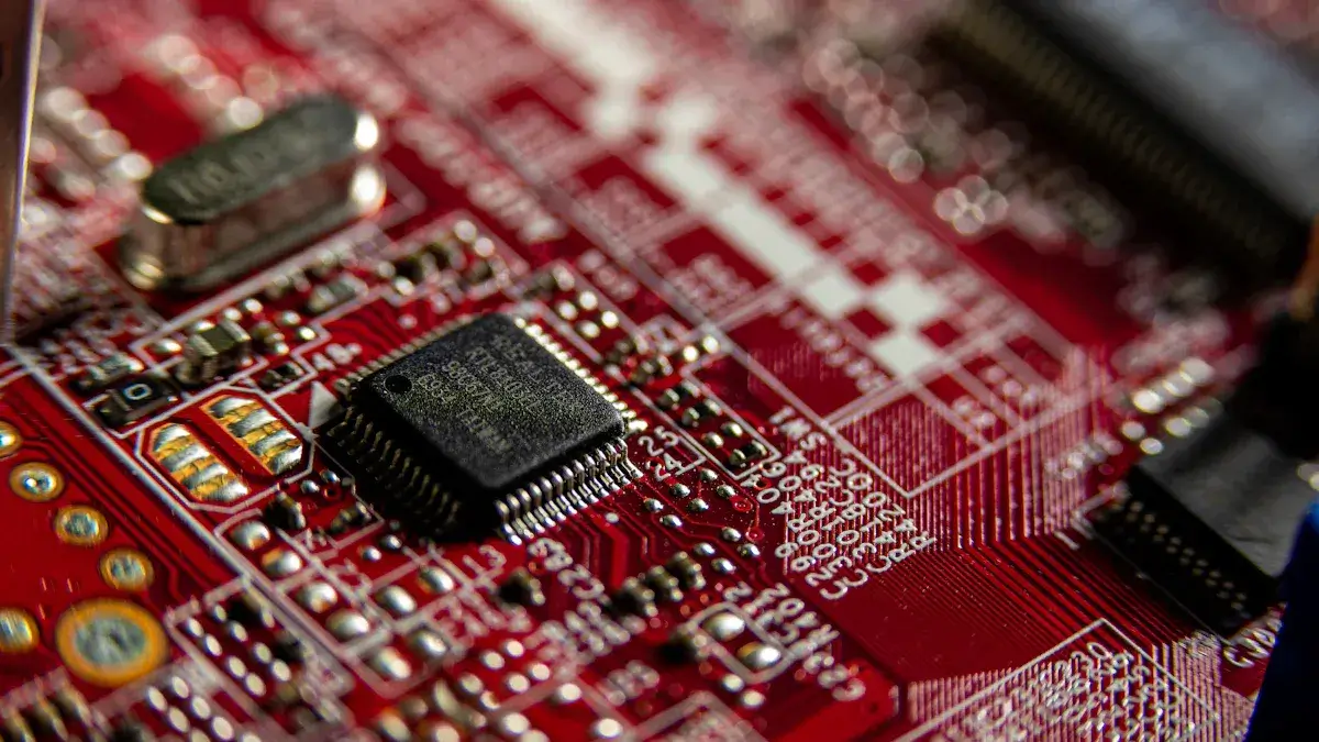
Automotive control boards may have multiple DNP or voltage variants and typically include serialized production, large connectors, and polarity-sensitive protection components. 3D AOI measures component orientation, lead and connector coplanarity, exposed solder geometry, and repeated placement offsets across serialized PCBs.
The major risks are variant confusion and local PCB deflection around connector areas. A correct board may be identified as defective when the program uses the wrong approved variant, while inadequate physical support can also create apparent coplanarity failures. SUGA links the AOI program to the PCB revision, approved variant, panel position, and accepted component set before confirmed patterns are used for placement or process corrections.
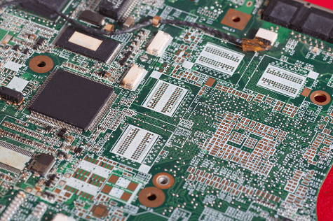
Medical Device PCB
Fine-pitch medical device assemblies are inspected for component height, position, polarity, connector seating, and visible solder contours. First-article qualification establishes the inspection reference for repeat production.
An optically corrected solder joint or component position does not confirm leakage performance, isolation, calibration, or electrical function. SUGA links the original AOI call, repair, reinspection, and all required electrical or functional retests through the board identifier. In addition, a footprint-compatible alternate is requalified when its component body height, marking, color, polarity cues, or terminal configuration changes.

Aerospace Electronics PCB
Aerospace electronics programs are often characterized by low production volumes, long service lives, repeated revision control, and substitutions for obsolete parts. The inspection program evaluates lifted leads, tilt, coplanarity variation, local board-plane deviation, foreign material, and connector or shield seating.
When an electrically accepted substitute has a different body height, surface marking, lead finish, or reflective characteristic, it requires its own optical model. Inspection sequencing is also important. Components that will be concealed by a shield are inspected before shield installation, while the later inspection confirms the height and seating of the shield. AOI images indicate the physical condition of accessible surfaces but do not confirm concealed joints or long-term reliability.
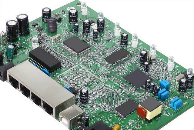
Consumer Electronics PCB
Consumer electronics PCBs can combine small packages, camera modules, reflective finishes, and other difficult optical features on one board, limiting the amount of stable optical information available for inspection. SUGA tunes the recipe by region and feature, detecting missing or incorrect parts, tombstoning, billboarding, bridges, and placement drift after reflow.
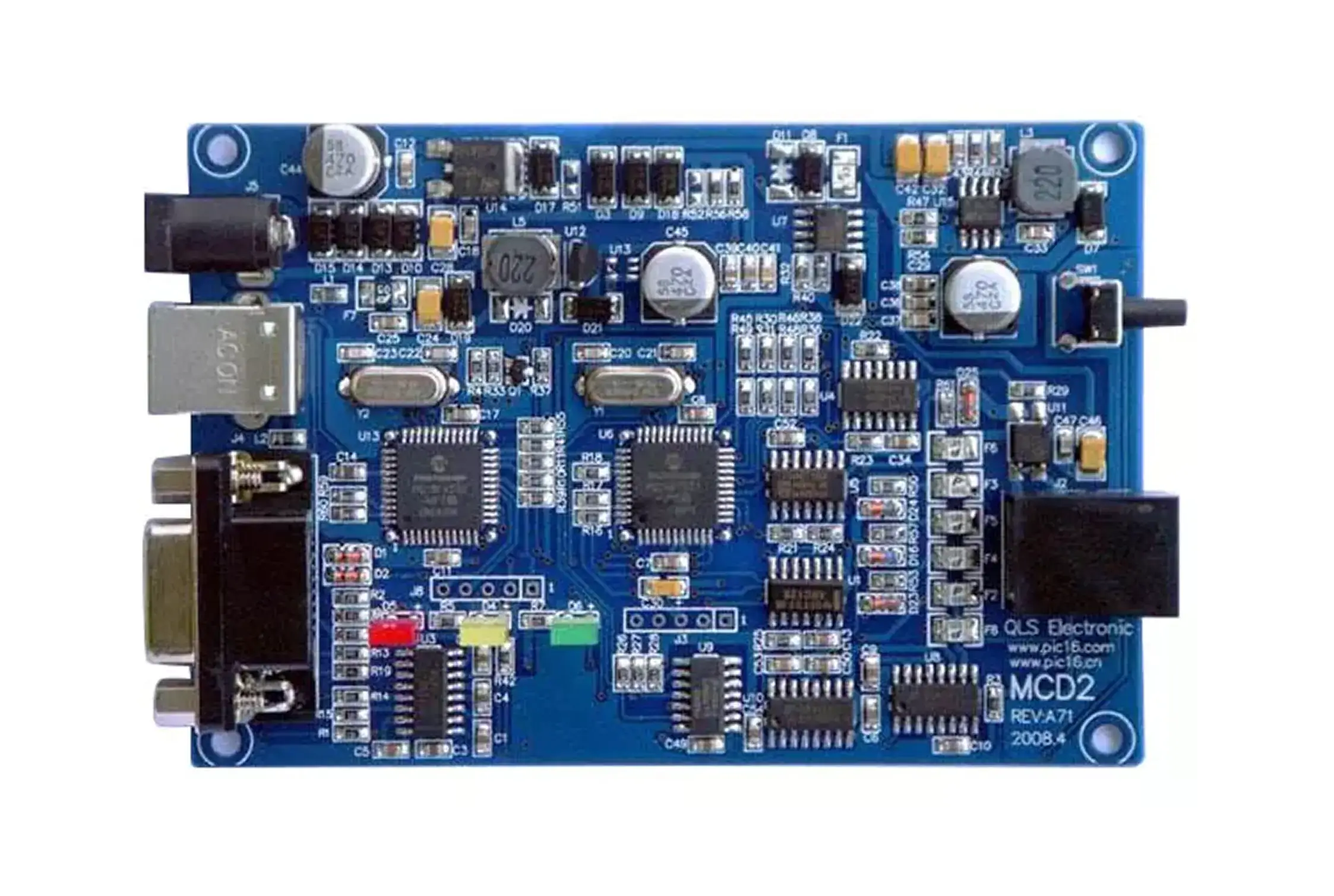
IoT Device PCB
IoT product designs can change so rapidly that an outdated feature reference may remain in the AOI library after a new part is introduced. For this reason, the SUGA program is created according to the approved BOM variant. Component position, body profile, connector geometry, visible solder geometry, and other traceable features are measured so discrepancies can be identified.
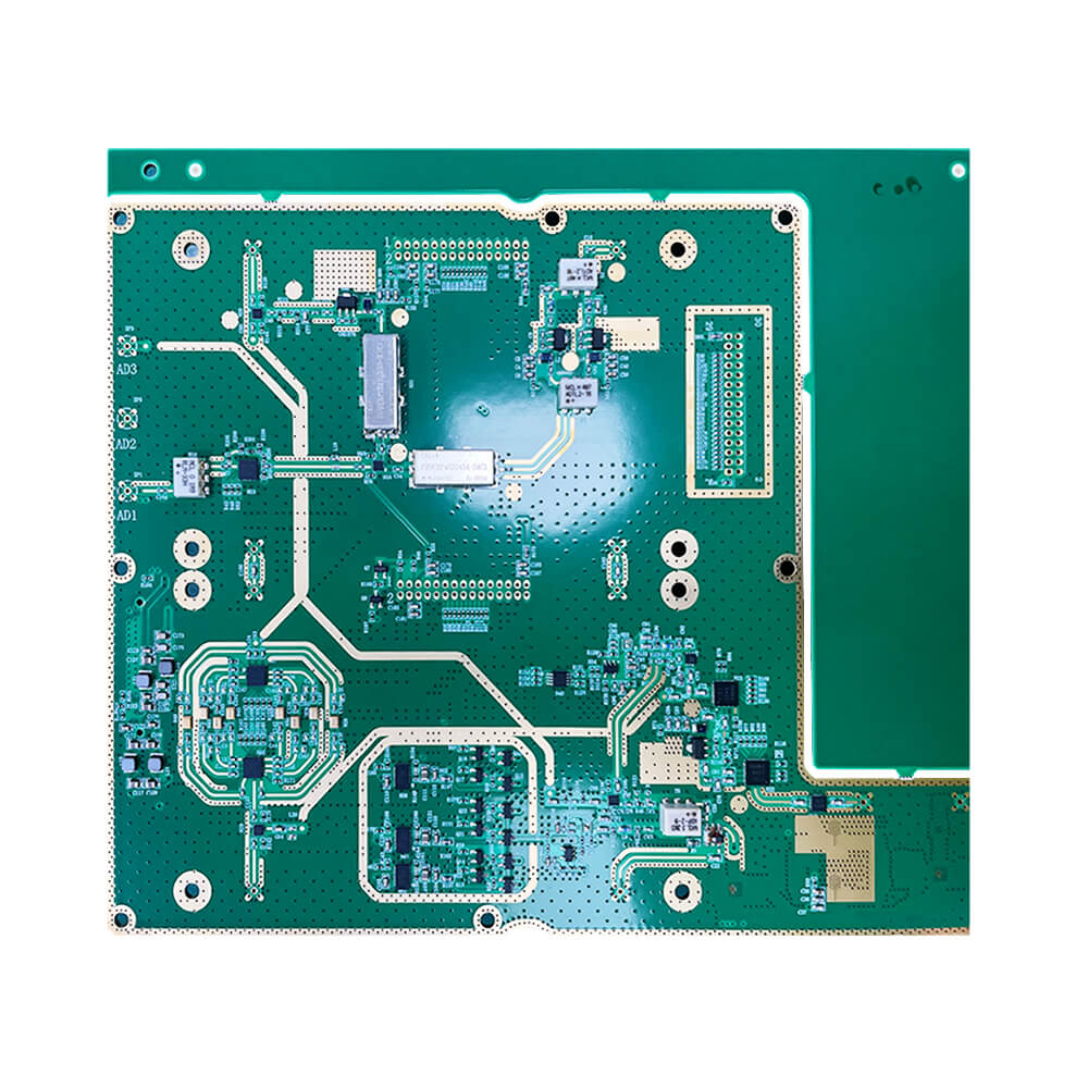
Industrial Automation PCB
Industrial automation PCBs combine surface mount devices with connectors and terminals that may become fully visible only after later assembly operations. A feature that passed an earlier inspection can also be affected during subsequent soldering or installation. SUGA measures polarity, position, height, seating, coplanarity, and visible solder geometry, then reinspects the relevant features after later operations.
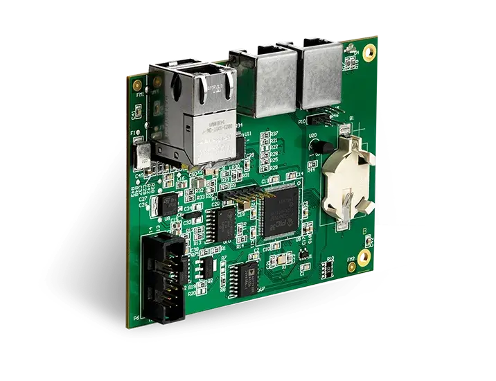
Telecommunications Equipment PCB
Telecommunications PCBs and circuit assemblies use multiple configurations and layouts for radio, switching, and backplane applications. SUGA uses 3D AOI to measure component position and rotation, exposed leads, connector coplanarity, and shield placement.
3D AOI verifies the body position of a BGA or QFN, while bottom-side joint geometry is verified using X-ray inspection. Components are inspected before shield installation, followed by confirmation of the shield position and height. Connector coplanarity can be visually measured, while contact resistance, radio-frequency performance, and signal integrity require separate testing.
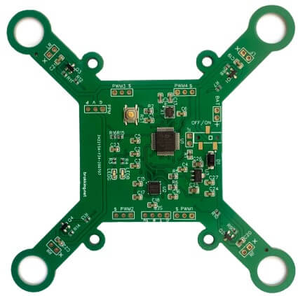
UAV Electronics PCB
Before UAV electronics enter mechanical integration, small placement errors can have greater consequences than in less position-sensitive assemblies. A small offset that may be cosmetic elsewhere can affect the alignment of an inertial measurement unit or GNSS module and influence later calibration.
3D AOI checks component polarity, sensor orientation, connector seating, small component offsets, visible board deformation, and foreign material before correction becomes more difficult after mechanical integration.
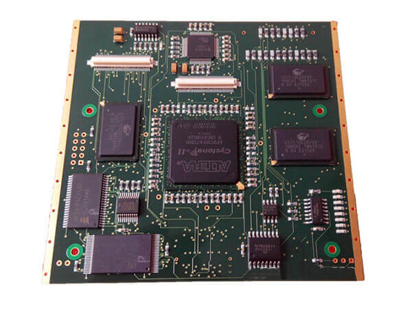
Robotics Control PCB
Robotics control PCBs used in motor and motor-drive applications can include encoders, sensors, communication circuits, large connectors, heat sinks, and mechanically tall components. 3D AOI verifies component placement, connector and lead coplanarity, exposed solder profiles, and repeated placement variation.
Heat sinks, shields, and structural hardware can create shadows that obscure MOSFETs, driver circuits, or nearby small components. Therefore, critical optical inspections are performed before mechanical installation, followed by an inspection that confirms the installed height and seating of the hardware. Recurring calls can identify conditions requiring program or process correction, while loaded motor-drive behavior, thermal performance, and sensor response remain outside the AOI conclusion.
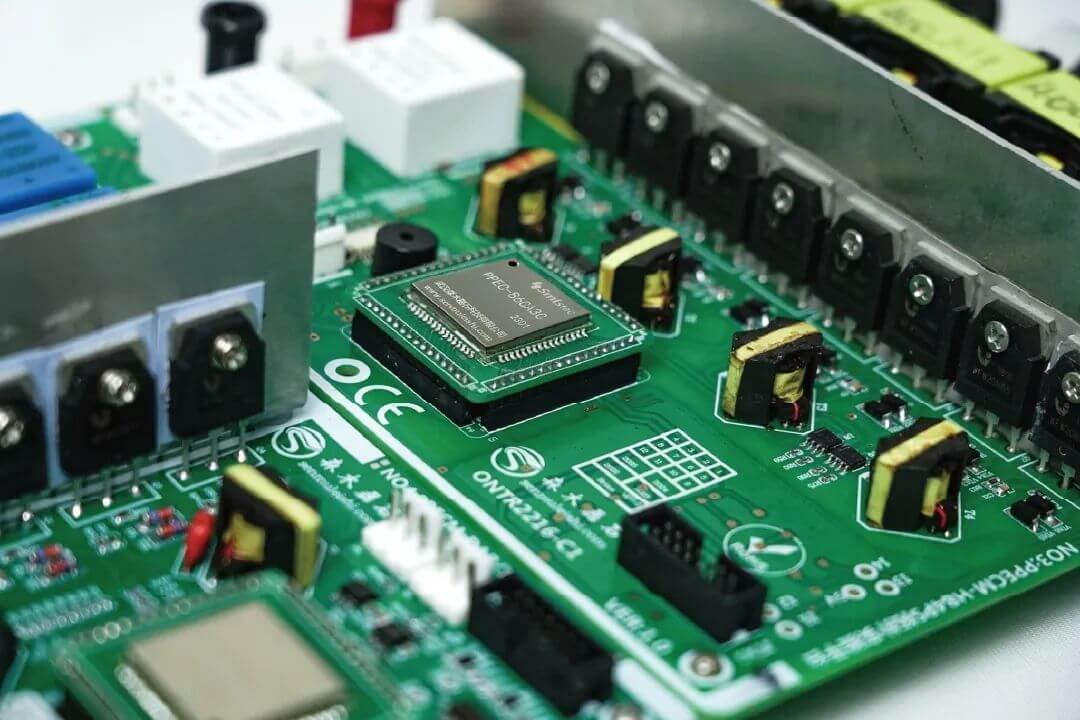
Power Electronics PCB
Power electronics PCBs place high-thermal-mass components next to fine control circuitry, so different regions may require different inspection tolerances. 3D AOI identifies missing or reversed components, seating-height and tilt errors, connector misalignment, and visible board deformation. Oversized components can also be evaluated against the programmed inspection envelope.
Our PCBA Production Lines
















Frequently Asked Questions
Using a golden board can support 3D AOI programming, but it is only one of several possible references. SUGA can also create an inspection program using approved Gerber or CAD files, BOM data, centroid coordinates, assembly drawings, component libraries, polarity references, variant and DNP information, and a known-good board or accepted first article. The selected reference set must match the same PCB/PCBA revision, package configuration, and approved alternates used in production.
Report changes to the manufacturer part number, approved alternate, package height, body color or finish, marking position, polarity cue, terminal geometry, DNP status, or supplier-lot appearance before production. A footprint-compatible alternate may not be optically equivalent. In these cases, SUGA updates the affected library, lighting, feature region, or threshold and confirms the revised component during first-article production before repeat production continues.
X-ray testing is necessary when an acceptance decision depends on concealed joint geometry, including BGA, QFN, or other bottom-terminated connections. Electrical or functional testing is required to verify continuity, powered behavior, leakage, communication, calibration, or recovery after repair. These results remain linked to the original AOI call rather than serving as substitutes for the visible measurement.
Yes. Depending on the product control plan and installed data interface, results can be retrieved by board serial number, panel ID, circuit position, production lot, AOI station, and program revision. The inspection record can link the inspected location, image or 3D view, measured value, confirmation decision, board action, repair, reinspection, and retest result so the history does not need to be reconstructed from separate logs.